一 : TPS2552-1中文资料

元器件交易网www.61k.com
www.ti.comSLVS841A–NOVEMBER2008–REVISEDDECEMBER2008
PRECISIONADJUSTABLECURRENT-LIMITEDPOWER-DISTRIBUTIONSWITCHES
FEATURES
±6%Current-LimitAccuracyat1.3A
MeetsUSBCurrent-LimitingRequirementsBackwardsCompatiblewithTPS2550/51
AdjustableCurrentLimit,75mA–1300mA(typ)Constant-Current(TPS2552/53)andLatch-off(TPS2552-1/53-1)Versions
FastOvercurrentResponse-2-μS(typ)85-m?High-SideMOSFET(DBVPackage)ReverseInput-OutputVoltageProtectionOperatingRange:2.5Vto6.5V
1-μAMaximumStandbySupplyCurrentBuilt-inSoft-Start
15kVESDProtectionperIEC61000-4-2(withExternalCapacitance)
?????
DESCRIPTION
TheTPS2552/53andTPS2552-1/53-1power-distributionswitchesareintendedforapplicationswhereprecisioncurrentlimitingisrequiredorheavycapacitiveloadsandshortcircuitsareencountered.Thesedevicesofferaprogrammablecurrent-limitthresholdbetween75mAand1.3A(typ)viaanexternalresistor.Current-limitaccuracyastightas+/-6%canbeachievedatthehighercurrent-limitsettings.Thepower-switchriseandfalltimesarecontrolledtominimizecurrentsurgesduringturnon/off.
TPS2552/53deviceslimittheoutputcurrenttoasafelevelbyswitchingintoaconstant-currentmodewhentheoutputloadexceedsthecurrent-limitthreshold.TPS2552-1/53-1devicesprovidecircuitbreakerfunctionalitybylatchingoffthepowerswitchduringovercurrentorreverse-voltagesituations.Aninternalreverse-voltagedetectioncomparatordisablesthepower-switchintheeventthattheoutputvoltageisdrivenhigherthantheinputtoprotectdevicesontheinputsideoftheswitch.Thelogicoutputassertslowduringovercurrentandreverse-voltageconditions.
Input
???????
APPLICATIONS
?????
USBPorts/HubsDigitalTV
Set-TopBoxesMobilePhonesVOIPPhones
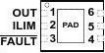
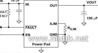
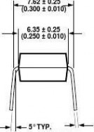
TIPS2552/TPS2553DRV??PACKAGE(TOPVIEW)
TIPS2552/TPS2553DBV??PACKAGE(TOPVIEW)
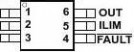
INENR

SignalPort
EN=Active??Low??for??the??TPS2552EN??=Active??High??for??the??TPS2553Add??-1??to??part??number??for??lach-off??version
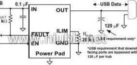
Figure1.TypicalApplicationasUSBPowerSwitch
Pleasebeawarethatanimportantnoticeconcerningavailability,standardwarranty,anduseincriticalapplicationsofTexasInstrumentssemiconductorproductsanddisclaimerstheretoappearsattheendofthisdatasheet.
PowerPADisatrademarkofTexasInstruments.
Copyright?2008,TexasInstrumentsIncorporated
PRODUCTIONDATAinformationiscurrentasofpublicationdate.ProductsconformtospecificationsperthetermsoftheTexasInstrumentsstandardwarranty.Productionprocessingdoesnotnecessarilyincludetestingofallparameters.

元器件交易网www.61k.comLVS841A–NOVEMBER2008–REVISEDDECEMBER2008www.ti.com
Thisdevicecontainscircuitstoprotectitsinputsandoutputsagainstdamageduetohighstaticvoltagesorelectrostaticfields.Thesecircuitshavebeenqualifiedtoprotectthisdeviceagainstelectrostaticdischarges(ESD)ofupto2kVaccordingtoMIL-STD-883C,Method3015;however,itisadvisedthatprecautionsbetakentoavoidapplicationofanyvoltagehigherthanmaximum-ratedvoltagestothesehigh-impedancecircuits.Duringstorageorhandlingthedeviceleadsshouldbeshortedtogetherorthedeviceshouldbeplacedinconductivefoam.Inacircuit,unusedinputsshouldalwaysbeconnectedtoanappropriatelogicvoltagelevel,preferablyeitherVCCorground.SpecificguidelinesforhandlingdevicesofthistypearecontainedinthepublicationGuidelinesforHandlingElectrostatic-Discharge-Sensitive(ESDS)DevicesandAssembliesavailablefromTexasInstruments.
AVAILABLEOPTIONSANDORDERINGINFORMATION
DEVICE(1)TPS2552TPS2553TPS2552-1TPS2553-1(1)(2)(3)
–40°Cto85°CAMBIENTTEMPERATURE
(2)
ENABLEActivelowActivehighActivelow
SON(3)(DRV)TPS2552DRVTPS2553DRVTPS2552DRV-1
SOT23(3)(DBV)TPS2552DBVTPS2553DBVTPS2552DBV-1TPS2553DBV-1
RECOMMENDEDMAXIMUM
CONTINUOUSLOAD
CURRENT
CURRENT-LIMITPROTECTIONConstant-Current
1.2A
Latch-Off
ActivehighTPS2553DRV-1
Forthemostcurrentpackageandorderinginformation,seethePackageOptionAddendumattheendofthisdocument,orseetheTIwebsiteatwww.ti.comMaximumambienttemperatureisafunctionofdevicejunctiontemperatureandsystemlevelconsiderations,suchaspowerdissipationandboardlayout.Seedissipationratingtableandrecommendedoperatingconditionsforspecificinformationrelatedtothesedevices.AddanRsuffixtothedevicetypefortapeandreel.
ABSOLUTEMAXIMUMRATINGS
overoperatingfree-airtemperaturerangeunlessotherwisenoted(1)
VoltagerangeonIN,OUT,ENorEN,ILIM,FAULTVoltagerangefromINtoOUT
IO
ContinuousoutputcurrentContinuoustotalpowerdissipationContinuoussinkcurrentILIMsourcecurrentESD
TJTstg(1)(2)
HBMCDM
(2)
VALUE–0.3to7–7to7InternallyLimitedSeetheDissipationRating
Table
2512500–40to150–65to150
UNITVV
mAmAkVV°C°C
MaximumjunctiontemperatureStoragetemperature
Stressesbeyondthoselistedunderabsolutemaximumratingsmaycausepermanentdamagetothedevice.Thesearestressratingsonly,andfunctionaloperationofthedeviceattheseoranyotherconditionsbeyondthoseindicatedunderrecommendedoperatingconditionsisnotimplied.Exposuretoabsolute-maximum-ratedconditionsforextendedperiodsmayaffectdevicereliability.VoltagesarereferencedtoGNDunlessotherwisenoted.
DISSIPATIONRATINGTABLE
BOARDLow-K(1)High-KLow-KHigh-K(1)(2)
(2)(1)(2)
PACKAGEDBVDBVDRVDRV
THERMALRESISTANCE
θJA
350°C/W160°C/W140°C/W75°C/W
THERMALRESISTANCE
θJC
55°C/W55°C/W20°C/W20°C/W
TA≤25°CPOWERRATING285mW625mW715mW1330mW
DERATINGFACTORABOVE
TA=25°C2.85mW/°C6.25mW/°C7.1mW/°C13.3mW/°C
TA=70°CPOWERRATING155mW340mW395mW730mW
TA=85°CPOWERRATING114mW250mW285mW530mW
TheJEDEClow-K(1s)boardusedtoderivethisdatawasa3in×3in,two-layerboardwith2-ouncecoppertracesontopoftheboard.TheJEDEChigh-K(2s2p)boardusedtoderivethisdatawasa3in×3in,multilayerboardwith1-ounceinternalpowerandgroundplanesand2-ouncecoppertracesontopandbottomoftheboard.
2SubmitDocumentationFeedbackCopyright?2008,TexasInstrumentsIncorporated
ProductFolderLink(s):TPS2552TPS2553TPS2552-1TPS2553-1
元器件交易网www.61k.com
www.ti.comSLVS841A–NOVEMBER2008–REVISEDDECEMBER2008
RECOMMENDEDOPERATINGCONDITIONS
MIN
VINVENV/ENVIHVILIOUTRILIMIO
Inputvoltage,INEnablevoltage
High-levelinputvoltageonENorLow-levelinputvoltageonENorContinuousoutputcurrent,OUT
Current-limitthresholdresistorrange(nominal1%)fromILIMtoGNDContinuoussinkcurrent
Inputde-couplingcapacitance,INtoGND
TJ
Operatingvirtualjunctiontemperature
DRVandDBV
019.100.1–40
125
TPS2552/52-1TPS2553/53-1
2.5001.1
0.661.223210MAX6.56.56.5
UNITVVVAk?mAμF°C
ELECTRICALCHARACTERISTICS
overrecommendedoperatingjunctiontemperaturerange,2.5V≤VIN≤6.5V,19.1k?≤RILIM≤232k?,V/EN=0V,orVEN=VIN,RFAULT=10k?(unlessotherwisenoted)
(1)
Pulse-testingtechniquesmaintainjunctiontemperatureclosetoambienttemperature;thermaleffectsmustbetakenintoaccountseparately.
Copyright?2008,TexasInstrumentsIncorporatedSubmitDocumentationFeedback3
ProductFolderLink(s):TPS2552TPS2553TPS2552-1TPS2553-1
元器件交易网www.61k.comLVS841A–NOVEMBER2008–REVISEDDECEMBER2008www.ti.com
ELECTRICALCHARACTERISTICS(continued)
overrecommendedoperatingjunctiontemperaturerange,2.5V≤VIN≤6.5V,19.1k?≤RILIM≤232k?,V/EN=0V,orVEN=VIN,RFAULT=10k?(unlessotherwisenoted)
PARAMETER
SUPPLYCURRENTIIN_offIIN_onIREVUVLO
Supplycurrent,low-leveloutputSupplycurrent,high-leveloutputReverseleakagecurrentLow-levelinputvoltage,INHysteresis,IN
FLAGVOL
Outputlowvoltage,Off-stateleakagedeglitch
THERMALSHUTDOWN
ThermalshutdownthresholdThermalshutdownthresholdincurrent-limitHysteresis
155135
10
°C°C°C
I/FAULT=1mAV/FAULT=6.5V
assertionorde-assertionduetoovercurrentconditionassertionorde-assertionduetoreverse-voltagecondition
52
7.54
1801106
mVμAmsms
VIN=6.5V,NoloadonOUT,VEN=6.5VorVEN=0VVIN=6.5V,NoloadonOUTVOUT=6.5V,VIN=0VVINrisingTJ=25°C
RILIM=20k?RILIM=210k?TJ=25°C
0.11201000.012.3525
114012012.45
μAμAμAμAVmV
TESTCONDITIONS(1)
MIN
TYP
MAX
UNIT
UNDERVOLTAGELOCKOUT
4SubmitDocumentationFeedbackCopyright?2008,TexasInstrumentsIncorporated
ProductFolderLink(s):TPS2552TPS2553TPS2552-1TPS2553-1
元器件交易网www.61k.com
www.ti.comSLVS841A–NOVEMBER2008–REVISEDDECEMBER2008
DEVICE

INFORMATION
PinFunctions
PIN
NAMEENGNDIN
TPS2552DBV
3–21
TPS2553DBV
–321
TPS2552DRV
4–56
TPS2553DRV
–456
II/OII
DESCRIPTION
Enableinput,logiclowturnsonpowerswitchEnableinput,logichighturnsonpowerswitchGroundconnection;connectexternallytoPowerPAD
Inputvoltage;connecta0.1μForgreater
ceramiccapacitorfromINtoGNDasclosetotheICaspossible.
Active-lowopen-drainoutput,assertedduringovercurrent,overtemperature,orreverse-voltageconditions.
Power-switchoutput
Externalresistorusedtosetcurrent-limit
threshold;recommended19.1k?≤RILIM≤232k?.
InternallyconnectedtoGND;usedtoheat-sinktheparttothecircuitboardtraces.ConnectPowerPADtoGNDpinexternally.
4433O
OUTILIM
65
65
12
12
OO
PowerPAD?
––PADPAD
Add-1forLatch-Offversion
FUNCTIONALBLOCKDIAGRAM
NoteA:TPS255x??parts??enter??constant??current??modeduring??current??limit??condition;TPS255x-1parts??latch??off
Copyright?2008,TexasInstrumentsIncorporatedSubmitDocumentationFeedback5
ProductFolderLink(s):TPS2552TPS2553TPS2552-1TPS2553-1
元器件交易网www.61k.comLVS841A–NOVEMBER2008–REVISEDDECEMBER2008www.ti.com
PARAMETERMEASUREMENTINFORMATION
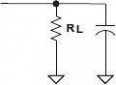
OUT
CL
VOUT
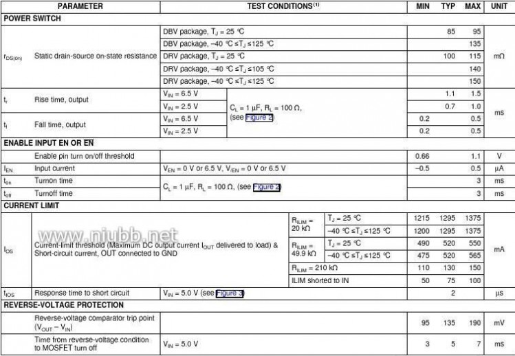
TEST??CIRCUIT

V
VVVOLTAGE??WAVEFORMS
Figure2.TestCircuitandVoltageWaveforms
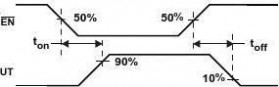
Figure3.Waveform
Decreasing
VIOUT
OS
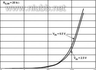
Figure4.OutputVoltagevs.Current-LimitThreshold
6SubmitDocumentationFeedbackCopyright?2008,TexasInstrumentsIncorporated
ProductFolderLink(s):TPS2552TPS2553TPS2552-1TPS2553-1
元器件交易网www.61k.comww.ti.comSLVS841A–NOVEMBER2008–REVISEDDECEMBER2008
TYPICALCHARACTERISTICS
R


Signal
Control??SignalTPS2552
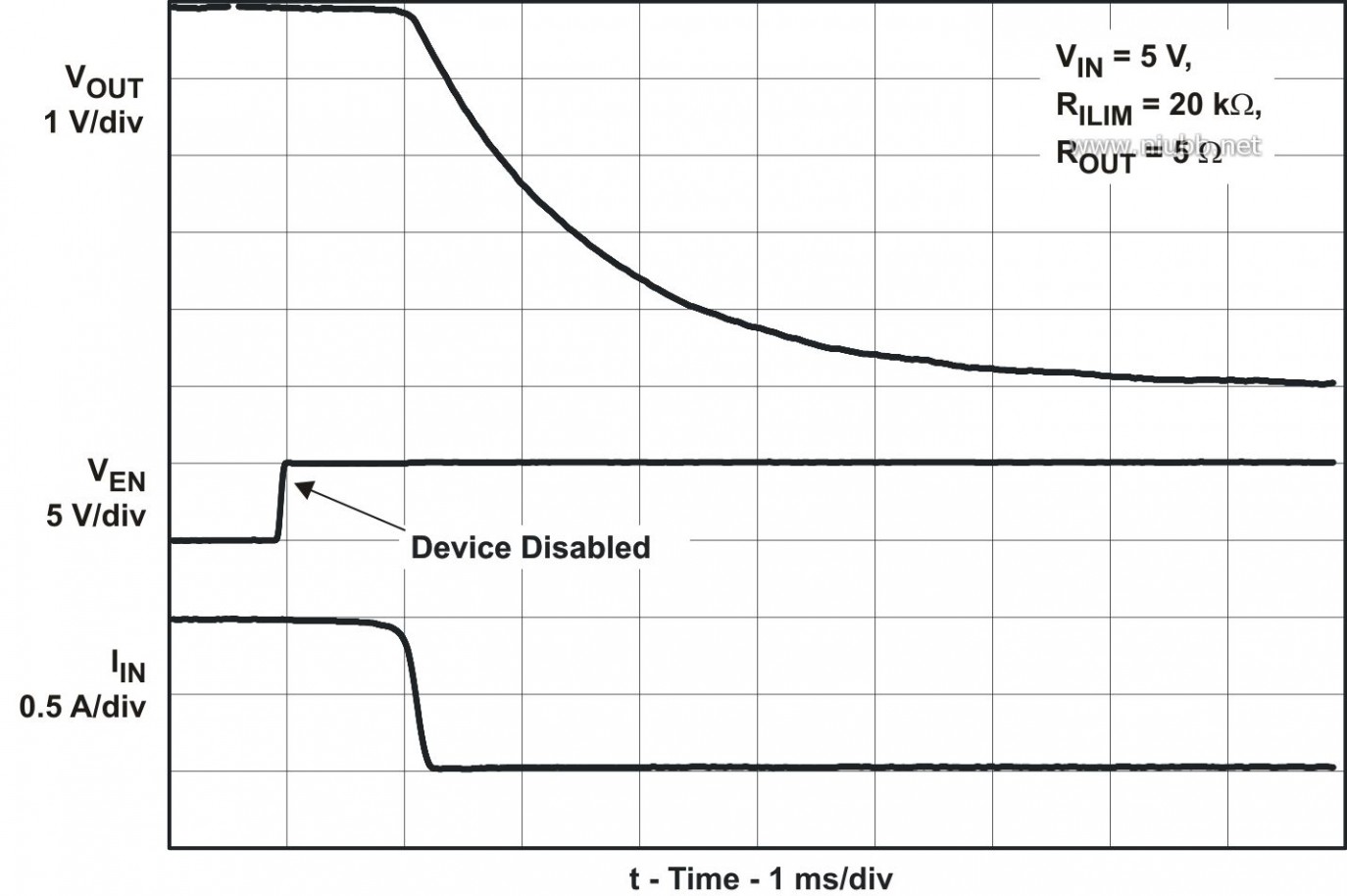
Figure5.TypicalCharacteristicsReferenceSchematic
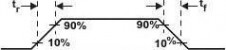
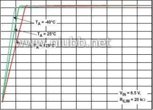
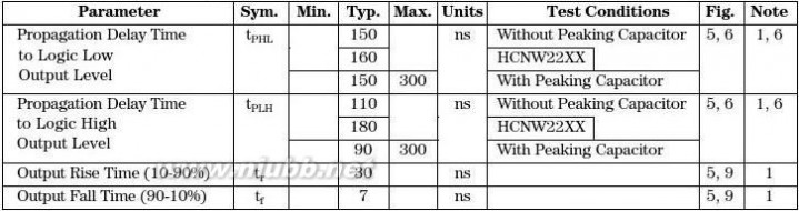
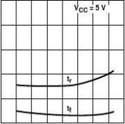
Figure6.TurnonDelayandRiseTimeFigure7.TurnoffDelayandFallTime
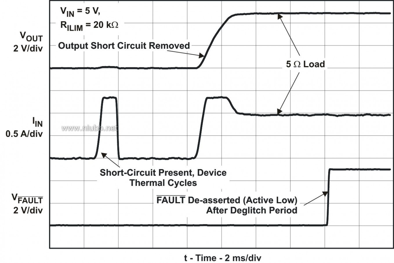
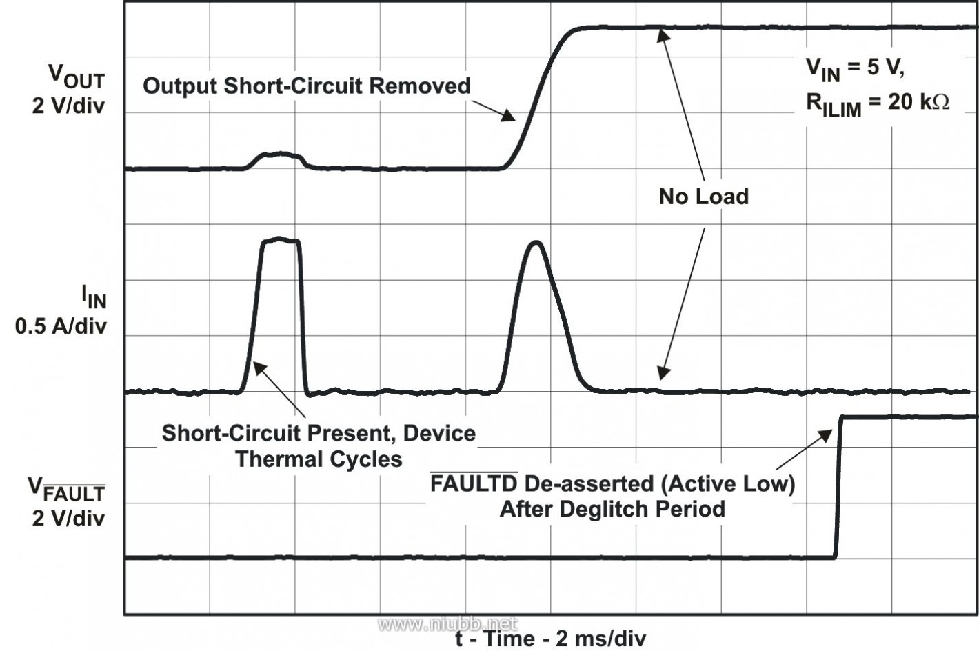
Figure8.DeviceEnabledintoShort-CircuitFigure9.Full-LoadtoShort-CircuitTransientResponseCopyright?2008,TexasInstrumentsIncorporatedSubmitDocumentationFeedback7
ProductFolderLink(s):TPS2552TPS2553TPS2552-1TPS2553-1

元器件交易网www.61k.comLVS841A–NOVEMBER2008–REVISEDDECEMBER2008www.ti.com
TYPICALCHARACTERISTICS(continued)
Figure10.Short-CircuittoFull-LoadRecoveryResponseFigure11.No-LoadtoShort-CircuitTransientResponseFigure12.Short-CircuittoNo-LoadRecoveryResponseFigure13.NoLoadto1?TransientResponseFigure14.1?toNoLoadTransientResponseFigure15.Reverse-VoltageProtectionResponse
8SubmitDocumentationFeedbackCopyright?2008,TexasInstrumentsIncorporated
ProductFolderLink(s):TPS2552TPS2553TPS2552-1TPS2553-1
元器件交易网www.61k.com
www.ti.comSLVS841A–NOVEMBER2008–REVISEDDECEMBER2008
TYPICALCHARACTERISTICS(continued)
UVLO??-??Undervoltage??Lockout??-??V
-50
50
TJ-??Junction??Temperature??-??°C
100150
Figure16.Reverse-VoltageProtectionRecovery
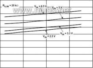
Figure17.UVLO–UndervoltageLockout–V
IIN-??Supply??Current,??Output??Disabled??-mA
IIN-??Supply??Current,??Output??Enabled??-mA
TJ-??Junction??Temperature??-??°C
TJ-??Junction??Temperature??-??°C
Figure18.IIN–SupplyCurrent,OutputDisabled–μA
201816

rDS(on)-??Static??Drain-Source??On-State??Resistance??-??mW
Figure19.IIN–SupplyCurrent,OutputEnabled–μA
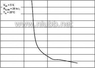
Current??Limit??Response??-ms
14121086420Peak??Current??-A
-50
50
TJ-??Junction??Temperature??-??°C
100150
Figure20.CurrentLimitResponse–μs
Figure21.MOSFETrDS(on)Vs.JunctionTemperature
Copyright?2008,TexasInstrumentsIncorporatedSubmitDocumentationFeedback9
ProductFolderLink(s):TPS2552TPS2553TPS2552-1TPS2553-1
元器件交易网www.61k.comLVS841A–NOVEMBER2008–REVISEDDECEMBER2008www.ti.com
TYPICALCHARACTERISTICS(continued)
1400
1300
IDS??-??Static??Drain-Source??Current??-??mA
IDS??-??Static??Drain-Source??Current??-??mA
1200110010009008007006005004003002001000VIN-??VOUT-??100??mV/div
100
200
300
400500600VIN-??VOUT-??100??mV/div
700
800
900
1000
Figure22.CurrentLimitThresholdVs.RILMFigure23.CurrentLimitThresholdVs.RILM
10SubmitDocumentationFeedbackCopyright?2008,TexasInstrumentsIncorporated
ProductFolderLink(s):TPS2552TPS2553TPS2552-1TPS2553-1
元器件交易网www.61k.comww.ti.comSLVS841A–NOVEMBER2008–REVISEDDECEMBER2008
DETAILEDDESCRIPTION
OVERVIEW
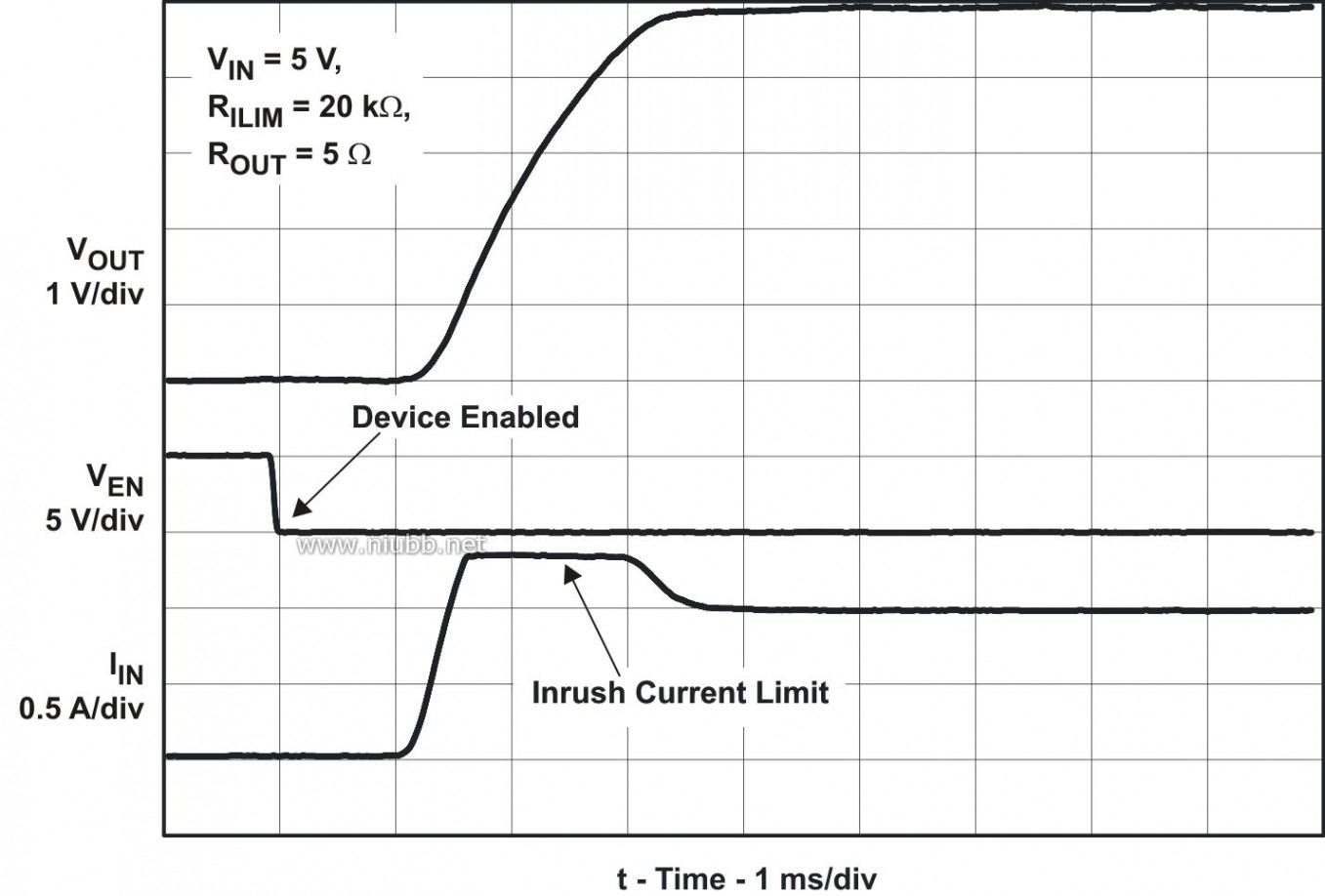
TheTPS2552/53andTPS2552-1/53-1arecurrent-limited,power-distributionswitchesusingN-channelMOSFETsforapplicationswhereshortcircuitsorheavycapacitiveloadswillbeencountered.Thesedevicesallowtheusertoprogramthecurrent-limitthresholdbetween75mAand1.3A(typ)viaanexternalresistor.Additionaldeviceshutdownfeaturesincludeovertemperatureprotectionandreverse-voltageprotection.ThedeviceincorporatesaninternalchargepumpandgatedrivecircuitrynecessarytodrivetheN-channelMOSFET.ThechargepumpsuppliespowertothedrivercircuitandprovidesthenecessaryvoltagetopullthegateoftheMOSFETabovethesource.Thechargepumpoperatesfrominputvoltagesaslowas2.5Vandrequireslittlesupplycurrent.Thedrivercontrolsthegatevoltageofthepowerswitch.Thedriverincorporatescircuitrythatcontrolstheriseandfalltimesoftheoutputvoltagetolimitlargecurrentandvoltagesurgesandprovidesbuilt-insoft-startfunctionality.Therearetwodevicefamiliesthathandleovercurrentsituationsdifferently.TheTPS2552/53familyentersconstant-currentmodewhiletheTPS2552-1/53-1familylatchesoffwhentheloadexceedsthecurrent-limitthreshold.
OVERCURRENTCONDITIONS
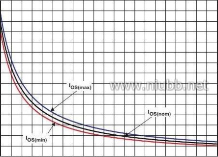
TheTPS2552/53andTPS2552-1/53-1respondtoovercurrentconditionsbylimitingtheiroutputcurrenttotheIOSlevelsshowninFigure24Whenanovercurrentconditionisdetected,thedevicemaintainsaconstantoutputcurrentandvoltageaccordingly.Twopossibleoverloadconditionscanoccur.
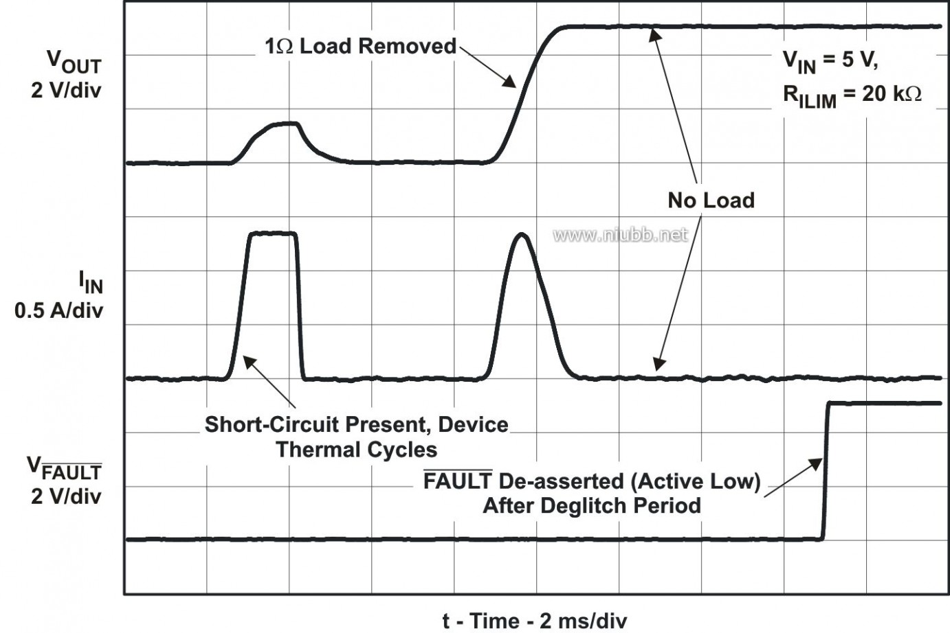
Thefirstconditioniswhenashortcircuitorpartialshortcircuitispresentwhenthedeviceispowered-uporenabled.TheoutputvoltageisheldnearzeropotentialwithrespecttogroundandtheTPS2552/53rampstheoutputcurrenttoIOS.TheTPS2552/53deviceswilllimitthecurrenttoIOSuntiltheoverloadconditionisremovedorthedevicebeginstothermalcycle.TheTPS2552-1/53-1deviceswilllimitthecurrenttoIOSuntiltheoverloadconditionisremovedortheinternaldeglitchtime(7.5-mstypical)isreachedandthedeviceisturnedoff.Thedevicewillremainoffuntilpoweriscycledorthedeviceenableistoggled.
Thesecondconditioniswhenashortcircuit,partialshortcircuit,ortransientoverloadoccurswhilethedeviceisenabledandpoweredon.ThedevicerespondstotheovercurrentconditionwithintimetIOS(seeFigure3Thecurrent-senseamplifierisoverdrivenduringthistimeandmomentarilydisablestheMOSFET.Thecurrent-senseamplifierrecoversandlimitstheoutputcurrenttoIOS.Similartothepreviouscase,theTPS2552/53willlimitthecurrenttoIOSuntiltheoverloadconditionisremovedorthedevicebeginstothermalcycle;theTPS2552-1/53-1willlimitthecurrenttoIOSuntiltheoverloadconditionisremovedortheinternaldeglitchtimeisreachedandthedeviceislatchedoff.
TheTPS2552/53thermalcyclesifanoverloadconditionispresentlongenoughtoactivatethermallimitinginanyoftheabovecases.Thedeviceturnsoffwhenthejunctiontemperatureexceeds135°C(typ)whileincurrentlimit.Thedeviceremainsoffuntilthejunctiontemperaturecools10°C(typ)andthenrestarts.TheTPS2552/53cycleson/offuntiltheoverloadisremoved(seeFigure10andFigure12.
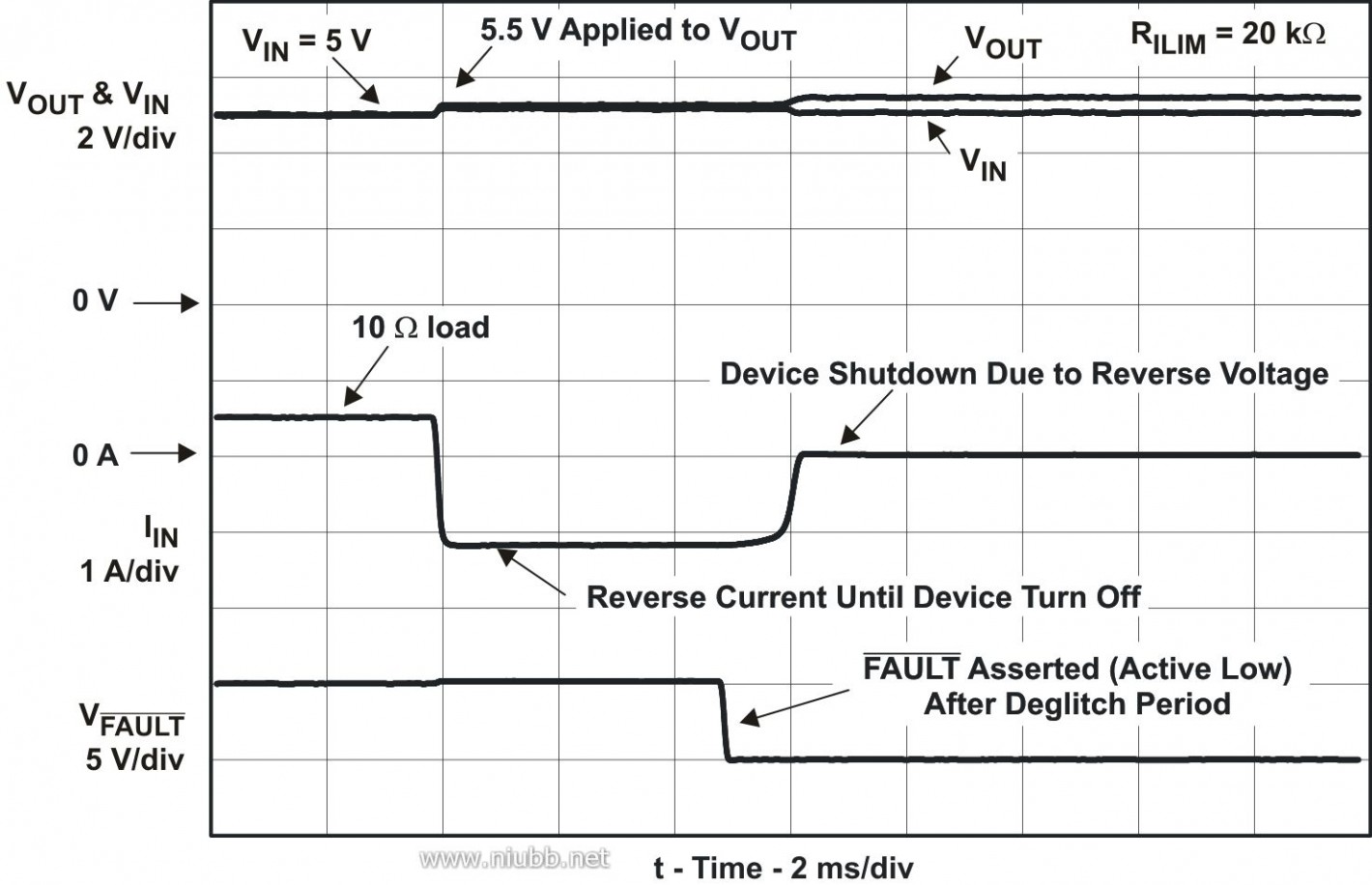
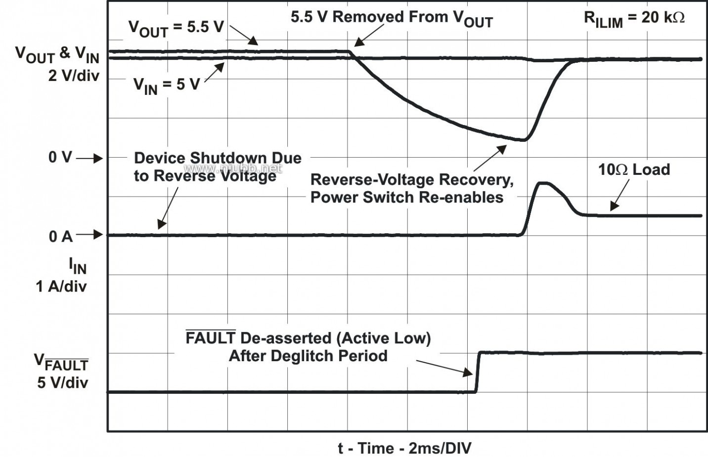
REVERSE-VOLTAGEPROTECTIONThereverse-voltageprotectionfeatureturnsofftheN-channelMOSFETwhenevertheoutputvoltageexceedstheinputvoltageby135mV(typ)for4-ms(typ).ThispreventsdamagetodevicesontheinputsideoftheTPS2552/53andTPS2552-1/TPS2253-1bypreventingsignificantcurrentfromsinkingintotheinputcapacitance.TheTPS2552/53devicesallowtheN-channelMOSFETtoturnononcetheoutputvoltagegoesbelowtheinputvoltageforthesame4-msdeglitchtime.TheTPS2552-1/53-1deviceskeepthedeviceturnedoffevenifthereverse-voltageconditionisremovedanddonotallowtheN-channelMOSFETtoturnonuntilpoweriscycledorthedeviceenableistoggled.Thereverse-voltagecomparatoralsoassertstheoutput(active-low)after4-ms.
Copyright?2008,TexasInstrumentsIncorporatedSubmitDocumentationFeedback11
ProductFolderLink(s):TPS2552TPS2553TPS2552-1TPS2553-1
元器件交易网www.61k.comLVS841A–NOVEMBER2008–REVISEDDECEMBER2008www.ti.comFAULTRESPONSE
Theopen-drainoutputisasserted(activelow)duringanovercurrent,overtemperatureorreverse-voltagecondition.TheTPS2552/53assertsthesignaluntilthefaultconditionisremovedandthedeviceresumesnormaloperation.TheTPS2552-1/53-1assertsthesignalduringafaultconditionandremainsassertedwhilethepartislatched-off.Thesignalisde-assertedoncedevicepoweriscycledortheenableistoggledandthedeviceresumesnormaloperation.TheTPS2552/53andTPS2552-1/53-1aredesignedtoeliminatefalsereportingbyusinganinternaldelay"deglitch"circuitforovercurrent(7.5-mstyp)andreverse-voltage(4-mstyp)conditionswithouttheneedforexternalcircuitry.Thisensuresthatisnotaccidentallyassertedduetonormaloperationsuchasstartingintoaheavycapacitiveload.Thedeglitchcircuitrydelaysenteringandleavingfaultconditions.Overtemperatureconditionsarenotdeglitchedandassertthesignalimmediately.
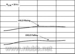
UNDERVOLTAGELOCKOUT(UVLO)
Theundervoltagelockout(UVLO)circuitdisablesthepowerswitchuntiltheinputvoltagereachestheUVLOturn-onthreshold.Built-inhysteresispreventsunwantedon/offcyclingduetoinputvoltagedropfromlargecurrentsurges.
ENABLEOREN)
Thelogicenablecontrolsthepowerswitch,biasforthechargepump,driver,andothercircuitstoreducethesupplycurrent.Thesupplycurrentisreducedtolessthan1-μAwhenalogichighispresentonorwhenalogiclowispresentonEN.AlogiclowinputonoralogichighinputonENenablesthedriver,controlcircuits,andpowerswitch.TheenableinputiscompatiblewithbothTTLandCMOSlogiclevels.
THERMALSENSETheTPS2552/53andTPS2552-1/53-1haveself-protectionfeaturesusingtwoindependentthermalsensingcircuitsthatmonitortheoperatingtemperatureofthepowerswitchanddisableoperationifthetemperatureexceedsrecommendedoperatingconditions.TheTPS2552/53deviceoperatesinconstant-currentmodeduringanovercurrentconditions,whichincreasesthevoltagedropacrosspower-switch.Thepowerdissipationinthepackageisproportionaltothevoltagedropacrossthepowerswitch,whichincreasesthejunctiontemperatureduringanovercurrentcondition.Thefirstthermalsensorturnsoffthepowerswitchwhenthedietemperatureexceeds135°C(min)andthepartisincurrentlimit.Hysteresisisbuiltintothethermalsensor,andtheswitchturnsonafterthedevicehascooledapproximately10°C.
TheTPS2552/53andTPS2552-1/53-1alsohaveasecondambientthermalsensor.Theambientthermalsensorturnsoffthepower-switchwhenthedietemperatureexceeds155°C(min)regardlessofwhetherthepowerswitchisincurrentlimitandwillturnonthepowerswitchafterthedevicehascooledapproximately10°C.BoththeTPS2552/53andTPS2552-1/53-1familiescontinuetocycleoffandonuntilthefaultisremoved.
Theopen-drainfaultreportingoutputisasserted(activelow)immediatelyduringanovertemperatureshutdowncondition.
12SubmitDocumentationFeedbackCopyright?2008,TexasInstrumentsIncorporated
ProductFolderLink(s):TPS2552TPS2553TPS2552-1TPS2553-1
元器件交易网www.61k.comww.ti.comSLVS841A–NOVEMBER2008–REVISEDDECEMBER2008
APPLICATIONINFORMATION
INPUTANDOUTPUTCAPACITANCE
Inputandoutputcapacitanceimprovestheperformanceofthedevice;theactualcapacitanceshouldbeoptimizedfortheparticularapplication.Forallapplications,a0.1μForgreaterceramicbypasscapacitorbetweenINandGNDisrecommendedasclosetothedeviceaspossibleforlocalnoisede-coupling.Thisprecautionreducesringingontheinputduetopower-supplytransients.Additionalinputcapacitancemaybeneededontheinputtoreducevoltageovershootfromexceedingtheabsolutemaximumvoltageofthedeviceduringheavytransientconditions.Thisisespeciallyimportantduringbenchtestingwhenlong,inductivecablesareusedtoconnecttheevaluationboardtothebenchpower-supply.
Placingahigh-valueelectrolyticcapacitorontheoutputpinisrecommendedwhenlargetransientcurrentsareexpectedontheoutput.Additionally,bypassingtheoutputwitha0.01μFto0.1μFceramiccapacitorimprovestheimmunityofthedevicetotransientconditionsandnoise.
PROGRAMMINGTHECURRENT-LIMITTHRESHOLD
Theovercurrentthresholdisuserprogrammableviaanexternalresistor.TheTPS2552/53andTPS2552-1/53-1useaninternalregulationlooptoprovidearegulatedvoltageontheILIMpin.Thecurrent-limitthresholdisproportionaltothecurrentsourcedoutofILIM.Therecommended1%resistorrangeforRILIMis19.1k?≤RILIM≤232k?toensurestabilityoftheinternalregulationloop.Manyapplicationsrequirethattheminimumcurrentlimitisaboveacertaincurrentlevelorthatthemaximumcurrentlimitisbelowacertaincurrentlevel,soitisimportanttoconsiderthetoleranceoftheovercurrentthresholdwhenselectingavalueforRILIM.ThefollowingequationsandFigure24canbeusedtocalculatetheresultingovercurrentthresholdforagivenexternalresistorvalue(RILIM).Figure24includescurrent-limittoleranceduetovariationscausedbytemperatureandprocess.However,thedonotaccountfortoleranceduetoexternalresistorvariation,soitisimportanttoaccountforthistolerancewhenselectingRILIM.ThetracesroutingtheRILIMresistortotheTPS2552/53andTPS2552-1/53-1shouldbeasshortaspossibletoreduceparasiticeffectsonthecurrent-limitaccuracy.RILIMcanbeselectedtoprovideacurrent-limitthresholdthatoccurs1)aboveaminimumloadcurrentor2)belowamaximumloadcurrent.
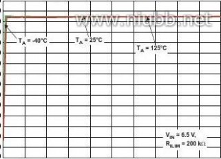
Todesignaboveaminimumcurrent-limitthreshold,findtheintersectionofRILIMandthemaximumdesiredloadcurrentontheIOS(min)curveandchooseavalueofRILIMbelowthisvalue.Programmingthecurrentlimitaboveaminimumthresholdisimportanttoensurestartupintofullloadorheavycapacitiveloads.Theresultingmaximumcurrent-limitthresholdistheintersectionoftheselectedvalueofRILIMandtheIOS(max)curve.
Todesignbelowamaximumcurrent-limitthreshold,findtheintersectionofRILIMandthemaximumdesiredloadcurrentontheIOS(max)curveandchooseavalueofRILIMabovethisvalue.Programmingthecurrentlimitbelowamaximumthresholdisimportanttoavoidcurrentlimitingupstreampowersuppliescausingtheinputvoltagebustodroop.Theresultingminimumcurrent-limitthresholdistheintersectionoftheselectedvalueofRILIMandtheIOS(min)curve.
Current-LimitThresholdEquations(IOS):
RILIM0.94kW
23950V
RILIM0.977kW
25230V
RILIM1.016kWIOSmax(mA)=IOSnom(mA)=IOSmin(mA)=(1)where19.1k?≤RILIM≤232k?.
WhilethemaximumrecommendedvalueofRILIMis232k?,thereisoneadditionalconfigurationthatallowsforalowercurrent-limitthreshold.TheILIMpinmaybeconnecteddirectlytoINtoprovidea75mA(typ)current-limitthreshold.Additionallow-ESRceramiccapacitancemaybenecessaryfromINtoGNDinthisconfigurationtopreventunwantednoisefromcouplingintothesensitiveILIMcircuitry.
Copyright?2008,TexasInstrumentsIncorporatedSubmitDocumentationFeedback13
ProductFolderLink(s):TPS2552TPS2553TPS2552-1TPS2553-1
元器件交易网www.61k.comLVS841A–NOVEMBER2008–REVISEDDECEMBER2008www.ti.com
1500
1400
1300
1200
Current??Limit??Threshold??-??mA11001000900800700600500
400
300
200
100
02030405060708090100110120130140150160170180190200210220
230RILIM-??Current??Limit??Resistor??-??kW
Figure24.Current-LimitThresholdvs.RILIM
14SubmitDocumentationFeedbackCopyright?2008,TexasInstrumentsIncorporated
ProductFolderLink(s):TPS2552TPS2553TPS2552-1TPS2553-1
元器件交易网www.61k.comww.ti.comSLVS841A–NOVEMBER2008–REVISEDDECEMBER2008APPLICATION1:DESIGNINGABOVEAMINIMUMCURRENTLIMIT
Someapplicationsrequirethatcurrentlimitingcannotoccurbelowacertainthreshold.Forthisexample,assumethat1Amustbedeliveredtotheloadsothattheminimumdesiredcurrent-limitthresholdis1000mA.UsetheIOSequationsandFigure24toselectRILIM.
IOSmin(mA)=1000mA
IOSmin(mA)=25230V
RILIM1.016kW
1?25230V?1.016÷÷RILIM(kW)=??÷?÷?èIOSminmA?RILIM(kW)=24kW(2)Selecttheclosest1%resistorlessthanthecalculatedvalue:RILIM=23.7k?.Thissetstheminimumcurrent-limitthresholdat1A.UsetheIOSequations,Figure24andthepreviouslycalculatedvalueforRILIMtocalculatethemaximumresultingcurrent-limitRILIM(kW)=23.7kW
IOSmax(mA)=
IOSmax(mA)=22980VRILIM0.94kW22980V
(3)23.70.94kWIOSmax(mA)=1172.4mA
Theresultingmaximumcurrent-limitthresholdis1172.4mAwitha23.7k?resistor.
APPLICATION2:DESIGNINGBELOWAMAXIMUMCURRENTLIMIT
Someapplicationsrequirethatcurrentlimitingmustoccurbelowacertainthreshold.Forthisexample,assumethatthedesireduppercurrent-limitthresholdmustbebelow500mAtoprotectanup-streampowersupply.UsetheIOSequationsandFigure24toselectRILIM.
IOSmax(mA)=500mA
IOSmax(mA)=22980V
RILIM0.94kW
1?22980V÷?0.94?÷RILIM(kW)=?÷??èIOSmaxmA÷?RILIM(kW)=58.7kW(4)Selecttheclosest1%resistorgreaterthanthecalculatedvalue:RILIM=59k?.Thissetsthemaximumcurrent-limitthresholdat500mA.UsetheIOSequations,Figure24andthepreviouslycalculatedvalueforRILIMtocalculatetheminimumresultingcurrent-limitthreshold.
RILIM(kW)=59kW
IOSmin(mA)=
IOSmin(mA)=25230VRILIM1.016kW25230V
(5)591.016kWIOSmin(mA)=400.6mA
Theresultingminimumcurrent-limitthresholdis400.6mAwitha59k?resistor.
Copyright?2008,TexasInstrumentsIncorporatedSubmitDocumentationFeedback15
ProductFolderLink(s):TPS2552TPS2553TPS2552-1TPS2553-1
元器件交易网www.61k.comLVS841A–NOVEMBER2008–REVISEDDECEMBER2008www.ti.com
ACCOUNTINGFORRESISTORTOLERANCE
TheprevioussectionsdescribedtheselectionofRILIMgivencertainapplicationrequirementsandtheimportanceofunderstandingthecurrent-limitthresholdtolerance.TheanalysisfocussedonlyontheTPS2552/53andTPS2552-1/53-1performanceandassumedanexactresistorvalue.However,resistorssoldinquantityarenotexactandareboundedbyanupperandlowertolerancecenteredaroundanominalresistance.TheadditionalRILIMresistancetolerancedirectlyaffectsthecurrent-limitthresholdaccuracyatasystemlevel.Thefollowingtableshowsaprocessthataccountsforworst-caseresistortoleranceassuming1%resistorvalues.Steponefollowstheselectionprocessoutlinedintheapplicationexamplesabove.Steptwodeterminestheupperandlowerresistanceboundsoftheselectedresistor.StepthreeusestheupperandlowerresistorboundsintheIOSequationstocalculatethethresholdlimits.Itisimportanttousetightertoleranceresistors,e.g.0.5%or0.1%,whenprecisioncurrentlimitingisdesired.
Table1.CommonRILIMResistorSelections
DesiredNominalCurrentLimit(mA)
751202003004005006007008009001000110012001300
226.1134.088.565.952.543.537.232.428.725.823.421.419.7IdealResistor(k?)
Closest1%Resistor(k?)
22613388.766.552.343.237.432.428.726.123.221.519.6
ResistorTolerance1%low(k?)
1%high(k?)
IOSMIN(mA)50.0
228.3134.389.667.252.843.637.832.729.026.423.421.719.8
101.3173.7262.1351.2448.3544.3630.2729.1824.7908.31023.71106.01215.1
ActualLimitsIOSNom(mA)75.0120.0201.5299.4396.7501.6604.6696.0800.8901.5989.11109.71195.41308.5
IOSMAX(mA)100.0142.1233.9342.3448.7562.4673.1770.8882.1988.71081.01207.51297.11414.9
SHORTILIMtoIN
223.7131.787.865.851.842.837.032.128.425.823.021.319.4
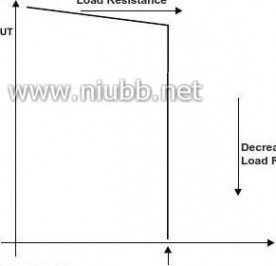
CONSTANT-CURRENTVS.LATCH-OFFOPERATIONANDIMPACTONOUTPUTVOLTAGE
Boththeconstant-currentdevices(TPS2552/53)andlatch-offdevices(TPS2552-1/53-1)operateidenticallyduringnormaloperation,i.e.theloadcurrentislessthanthecurrent-limitthresholdandthedevicesarenotlimitingcurrent.DuringnormaloperationtheN-channelMOSFETisfullyenhanced,andVOUT=VIN-(IOUTxrDS(on)).ThevoltagedropacrosstheMOSFETisrelativelysmallcomparedtoVIN,andVOUT≈VIN.
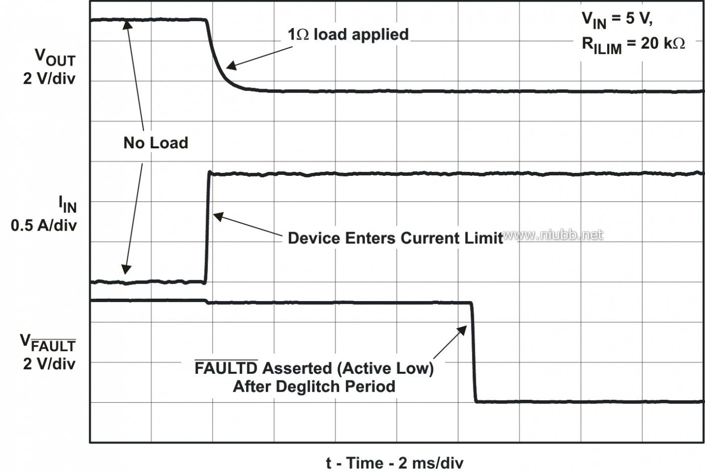
Boththeconstant-currentdevices(TPS2552/53)andlatch-offdevices(TPS2552-1/53-1)operateidenticallyduringtheinitialonsetofanovercurrentevent.Bothdeviceslimitcurrenttotheprogrammedcurrent-limitthresholdsetbyRILIMbyoperatingtheN-channelMOSFETinthelinearmode.Duringcurrent-limitoperation,theN-channelMOSFETisnolongerfully-enhancedandtheresistanceofthedeviceincreases.Thisallowsthedevicetoeffectivelyregulatethecurrenttothecurrent-limitthreshold.TheeffectofincreasingtheresistanceoftheMOSFETisthatthevoltagedropacrossthedeviceisnolongernegligible(VIN≠VOUT),andVOUTdecreases.TheamountthatVOUTdecreasesisproportionaltothemagnitudeoftheoverloadcondition.TheexpectedVOUTcanbecalculatedbyIOS×RLOAD,whereIOSisthecurrent-limitthresholdandRLOADisthemagnitudeoftheoverloadcondition.Forexample,ifIOSisprogrammedto1Aanda1?overloadconditionisapplied,theresultingVOUTis1V.
Whileboththeconstant-currentdevices(TPS2552/53)andlatch-offdevices(TPS2552-1/53-1)operateidenticallyduringtheinitialonsetofanovercurrentevent,theybehavedifferentlyiftheovercurrenteventlastslongerthantheinternaldelay"deglitch"circuit(7.5-mstyp).Theconstant-currentdevices(TPS2552/53)asserttheflagafterthedeglitchperiodandcontinuetoregulatethecurrenttothecurrent-limitthresholdindefinitely.Inpracticalcircuits,thepowerdissipationinthepackagewillincreasethedietemperatureabovetheovertemperatureshutdownthreshold(135°Cmin),andthedevicewillturnoffuntilthedietemperaturedecreasesbythehysteresisofthethermalshutdowncircuit(10°Ctyp).Thedevicewillturnonandcontinuetothermalcycle
16
SubmitDocumentationFeedback
Copyright?2008,TexasInstrumentsIncorporated
ProductFolderLink(s):TPS2552TPS2553TPS2552-1TPS2553-1
元器件交易网www.61k.comww.ti.comSLVS841A–NOVEMBER2008–REVISEDDECEMBER2008untiltheoverloadconditionisremoved.Theconstant-currentdevicesresumenormaloperationoncetheoverloadconditionisremoved.Thelatch-offdevices(TPS2552-1/53-1)asserttheflagafterthedeglitchperiodandimmediatelyturnoffthedevice.Thedeviceremainsoffregardlessofwhethertheoverloadconditionisremovedfromtheoutput.Thelatch-offdevicesremainoffanddonotresumenormaloperationuntilthesurroundingsystemeithertogglestheenableorcyclespowertothedevice.
POWERDISSIPATIONANDJUNCTIONTEMPERATUREThelowon-resistanceoftheN-channelMOSFETallowssmallsurface-mountpackagestopasslargecurrents.Itisgooddesignpracticetoestimatepowerdissipationandjunctiontemperature.Thebelowanalysisgivesanapproximationforcalculatingjunctiontemperaturebasedonthepowerdissipationinthepackage.However,itisimportanttonotethatthermalanalysisisstronglydependentonadditionalsystemlevelfactors.Suchfactorsincludeairflow,boardlayout,copperthicknessandsurfacearea,andproximitytootherdevicesdissipatingpower.Goodthermaldesignpracticemustincludeallsystemlevelfactorsinadditiontoindividualcomponentanalysis.
BeginbydeterminingtherDS(on)oftheN-channelMOSFETrelativetotheinputvoltageandoperatingtemperature.Asaninitialestimate,usethehighestoperatingambienttemperatureofinterestandreadrDS(on)fromthetypicalcharacteristicsgraph.Usingthisvalue,thepowerdissipationcanbecalculatedby:PD=rDS(on)×IOUT2
Where:
PD=Totalpowerdissipation(W)
rDS(on)=Powerswitchon-resistance(?)
IOUT=Maximumcurrent-limitthreshold(A)
ThisstepcalculatesthetotalpowerdissipationoftheN-channelMOSFET.
Finally,calculatethejunctiontemperature:
TJ=PD×θJA+TA
Copyright?2008,TexasInstrumentsIncorporatedSubmitDocumentationFeedback17
ProductFolderLink(s):TPS2552TPS2553TPS2552-1TPS2553-1
元器件交易网www.61k.comLVS841A–NOVEMBER2008–REVISEDDECEMBER2008www.ti.comWhere:
TA=Ambienttemperature(°C)
θJA=Thermalresistance(°C/W)
PD=Totalpowerdissipation(W)
Comparethecalculatedjunctiontemperaturewiththeinitialestimate.Iftheyarenotwithinafewdegrees,repeatthecalculationusingthe"refined"rDS(on)fromthepreviouscalculationasthenewestimate.Twoorthreeiterationsaregenerallysufficienttoachievethedesiredresult.ThefinaljunctiontemperatureishighlydependentonthermalresistanceθJA,andthermalresistanceishighlydependentontheindividualpackageandboardlayout.TheDissipatingRatingTableexamplethermalresistancesforspecificpackagesandboardlayouts.
UNIVERSALSERIALBUS(USB)POWER-DISTRIBUTIONREQUIREMENTSOneapplicationforthisdeviceisforcurrentlimitinginuniversalserialbus(USB)applications.TheoriginalUSBinterfacewasa12-Mb/sor1.5-Mb/s,multiplexedserialbusdesignedforlow-to-mediumbandwidthPCperipherals(e.g.,keyboards,printers,scanners,andmice).Asthedemandformorebandwidthincreased,theUSB2.0standardwasintroducedincreasingthemaximumdatarateto480-Mb/s.Thefour-wireUSBinterfaceisconceivedfordynamicattach-detach(hotplug-unplug)ofperipherals.Twolinesareprovidedfordifferentialdata,andtwolinesareprovidedfor5-Vpowerdistribution.
USBdataisa3.3-Vlevelsignal,butpowerisdistributedat5Vtoallowforvoltagedropsincaseswherepowerisdistributedthroughmorethanonehubacrosslongcables.Eachfunctionmustprovideitsownregulated3.3Vfromthe5-Vinputoritsowninternalpowersupply.TheUSBspecificationclassifiestwodifferentclassesofdevicesdependingonitsmaximumcurrentdraw.Adeviceclassifiedaslow-powercandrawupto100mAasdefinedbythestandard.Adeviceclassifiedashigh-powercandrawupto500mA.Itisimportantthattheminimumcurrent-limitthresholdofthecurrent-limitingpower-switchexceedthemaximumcurrent-limitdrawoftheintendedapplication.ThelatestUSBstandardshouldalwaysbereferencedwhenconsideringthecurrent-limitthreshold
TheUSBspecificationdefinestwotypesofdevicesashubsandfunctions.AUSBhubisadevicethatcontainsmultipleportsfordifferentUSBdevicestoconnectandcanbeself-powered(SPH)orbus-powered(BPH).AfunctionisaUSBdevicethatisabletotransmitorreceivedataorcontrolinformationoverthebus.AUSBfunctioncanbeembeddedinaUSBhub.AUSBfunctioncanbeoneofthreetypesincludedinthelistbelow.?Low-power,bus-poweredfunction
?High-power,bus-poweredfunction
?Self-poweredfunction
SPHsandBPHsdistributedataandpowertodownstreamfunctions.TheTPS2552/53hashighercurrentcapabilitythanrequiredforasingleUSBportallowingittopowermultipledownstreamports.
18SubmitDocumentationFeedbackCopyright?2008,TexasInstrumentsIncorporated
ProductFolderLink(s):TPS2552TPS2553TPS2552-1TPS2553-1
元器件交易网www.61k.comww.ti.comSLVS841A–NOVEMBER2008–REVISEDDECEMBER2008SELF-POWEREDANDBUS-POWEREDHUBS
ASPHhasalocalpowersupplythatpowersembeddedfunctionsanddownstreamports.Thispowersupplymustprovidebetween4.75Vto5.25Vtodownstreamfacingdevicesunderfull-loadandno-loadconditions.SPHsarerequiredtohavecurrent-limitprotectionandmustreportovercurrentconditionstotheUSBcontroller.TypicalSPHsaredesktopPCs,monitors,printers,andstand-alonehubs.
ABPHobtainsallpowerfromanupstreamportandoftencontainsanembeddedfunction.Itmustpowerupwithlessthan100mA.TheBPHusuallyhasoneembeddedfunction,andpowerisalwaysavailabletothecontrollerofthehub.Iftheembeddedfunctionandhubrequiremorethan100mAonpowerup,thepowertotheembeddedfunctionmayneedtobekeptoffuntilenumerationiscompleted.Thisisaccomplishedbyremovingpowerorbyshuttingofftheclocktotheembeddedfunction.Powerswitchingtheembeddedfunctionisnotnecessaryiftheaggregatepowerdrawforthefunctionandcontrollerislessthan100mA.Thetotalcurrentdrawnbythebus-powereddeviceisthesumofthecurrenttothecontroller,theembeddedfunction,andthedownstreamports,anditislimitedto500mAfromanupstreamport.
LOW-POWERBUS-POWEREDANDHIGH-POWERBUS-POWEREDFUNCTIONS
Bothlow-powerandhigh-powerbus-poweredfunctionsobtainallpowerfromupstreamports.Low-powerfunctionsalwaysdrawlessthan100mA;high-powerfunctionsmustdrawlessthan100mAatpowerupandcandrawupto500mAafterenumeration.Iftheloadofthefunctionismorethantheparallelcombinationof44?and10μFatpowerup,thedevicemustimplementinrushcurrentlimiting.
USBPOWER-DISTRIBUTIONREQUIREMENTSUSBcanbeimplementedinseveralwaysregardlessofthetypeofUSBdevicebeingdeveloped.Severalpower-distributionfeaturesmustbeimplemented.
?SPHsmust:
–Currentlimitdownstreamports
–Reportovercurrentconditions
?BPHsmust:
–Enable/disablepowertodownstreamports
–Powerupat<100mA
–Limitinrushcurrent(<44?and10μF)
?Functionsmust:
–Limitinrushcurrents
–Powerupat<100mA
ThefeaturesetoftheTPS2552/53andTPS2552-1/53-1meetseachoftheserequirements.Theintegratedcurrentlimitingandovercurrentreportingisrequiredbyself-poweredhubs.Thelogic-levelenableandcontrolledrisetimesmeettheneedofbothinputandoutputportsonbus-poweredhubsandtheinputportsforbus-poweredfunctions.
Copyright?2008,TexasInstrumentsIncorporatedSubmitDocumentationFeedback19
ProductFolderLink(s):TPS2552TPS2553TPS2552-1TPS2553-1
元器件交易网www.61k.comLVS841A–NOVEMBER2008–REVISEDDECEMBER2008www.ti.com
AUTO-RETRYFUNCTIONALITY
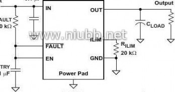
Someapplicationsrequirethatanovercurrentconditiondisablesthepartmomentarilyduringafaultconditionandre-enablesafterapre-settime.Thisauto-retryfunctionalitycanbeimplementedwithanexternalresistorandcapacitor.Duringafaultcondition,pullslowdisablingthepart.ThepartisdisabledwhenENispulledlow,andgoeshighimpedanceallowingCRETRYtobegincharging.Thepartre-enableswhenthevoltageonENreachestheturnonthreshold,andtheauto-retrytimeisdeterminedbytheresistor/capacitortimeconstant.Thepartwillcontinuetocycleinthismanneruntilthefaultconditionisremoved.
RC
LOAD

Figure25.Auto-RetryFunctionality
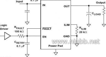
Someapplicationsrequireauto-retryfunctionalityandtheabilitytoenable/disablewithanexternallogicsignal.ThefigurebelowshowshowanexternallogicsignalcandriveENthroughRFAULTandmaintainauto-retryfunctionality.Theresistor/capacitortimeconstantdeterminestheauto-retrytime-outperiod.
TPS2553
LOAD
Signal&Figure26.Auto-RetryFunctionalityWithExternalENSignal
20SubmitDocumentationFeedbackCopyright?2008,TexasInstrumentsIncorporated
ProductFolderLink(s):TPS2552TPS2553TPS2552-1TPS2553-1
元器件交易网www.61k.comww.ti.comSLVS841A–NOVEMBER2008–REVISEDDECEMBER2008TWO-LEVELCURRENT-LIMITCIRCUIT

Someapplicationsrequiredifferentcurrent-limitthresholdsdependingonexternalsystemconditions.Figure27showsanimplementationforanexternallycontrolled,two-levelcurrent-limitcircuit.Thecurrent-limitsetbythetotalresistancefromILIMtoGND(seepreviouslydiscussed"ProgrammingtheCurrent-LimitThreshold"section).Alogic-levelinputenables/disablesMOSFETQ1andchangesthecurrent-limitthresholdbymodifyingthetotalresistancefromILIMtoGND.AdditionalMOSFET/resistorcombinationscanbeusedinparalleltoQ1/R2toincreasethenumberofadditionalcurrent-limitlevels.
NOTE:
ILIMshouldneverbedrivendirectlywithanexternalsignal.
RSignal
Control??SignalRLOADFigure27.Two-LevelCurrent-LimitCircuit
Copyright?2008,TexasInstrumentsIncorporatedSubmitDocumentationFeedback21
ProductFolderLink(s):TPS2552TPS2553TPS2552-1TPS2553-1
元器件交易网www.61k.com
PACKAGEOPTIONADDENDUM
www.ti.com
16-Dec-2008
PACKAGINGINFORMATION
OrderableDeviceTPS2552DBVRTPS2552DBVR-1TPS2552DBVTTPS2552DBVT-1TPS2552DRVRTPS2552DRVR-1TPS2552DRVTTPS2552DRVT-1TPS2553DBVRTPS2553DBVR-1TPS2553DBVTTPS2553DBVT-1TPS2553DRVRTPS2553DRVR-1TPS2553DRVTTPS2553DRVT-1
(1)
Status(1)ACTIVEACTIVEACTIVEACTIVEACTIVEACTIVEACTIVEACTIVEACTIVEACTIVEACTIVE

ACTIVEACTIVEACTIVEACTIVEACTIVE
PackageTypeSOT-23SOT-23SOT-23SOT-23SONSONSONSONSOT-23SOT-23SOT-23SOT-23SONSONSONSON
PackageDrawingDBVDBVDBVDBVDRVDRVDRVDRVDBVDBVDBVDBVDRVDRVDRVDRV
PinsPackageEcoPlan(2)
Qty6666666666666666
3000Green(RoHS&
noSb/Br)3000Green(RoHS&
noSb/Br)250250
Green(RoHS&noSb/Br)Green(RoHS&noSb/Br)
Lead/BallFinishCUNIPDAUCUNIPDAUCUNIPDAUCUNIPDAUCUNIPDAUCUNIPDAUCUNIPDAUCUNIPDAUCUNIPDAUCUNIPDAUCUNIPDAUCUNIPDAUCUNIPDAUCUNIPDAUCUNIPDAUCUNIPDAU
MSLPeakTemp(3)Level-1-260C-UNLIMLevel-1-260C-UNLIMLevel-1-260C-UNLIMLevel-1-260C-UNLIMLevel-1-260C-UNLIMLevel-1-260C-UNLIMLevel-1-260C-UNLIMLevel-1-260C-UNLIMLevel-1-260C-UNLIMLevel-1-260C-UNLIMLevel-1-260C-UNLIMLevel-1-260C-UNLIMLevel-1-260C-UNLIMLevel-1-260C-UNLIMLevel-1-260C-UNLIMLevel-1-260C-UNLIM
3000Green(RoHS&
noSb/Br)3000Green(RoHS&
noSb/Br)250250
Green(RoHS&noSb/Br)Green(RoHS&noSb/Br)
3000Green(RoHS&
noSb/Br)3000Green(RoHS&
noSb/Br)250250
Green(RoHS&noSb/Br)Green(RoHS&noSb/Br)
3000Green(RoHS&
noSb/Br)3000Green(RoHS&
noSb/Br)250250
Green(RoHS&noSb/Br)Green(RoHS&noSb/Br)
Themarketingstatusvaluesaredefinedasfollows:ACTIVE:Productdevicerecommendedfornewdesigns.
LIFEBUY:TIhasannouncedthatthedevicewillbediscontinued,andalifetime-buyperiodisineffect.
NRND:Notrecommendedfornewdesigns.Deviceisinproductiontosupportexistingcustomers,butTIdoesnotrecommendusingthispartinanewdesign.
PREVIEW:Devicehasbeenannouncedbutisnotinproduction.Samplesmayormaynotbeavailable.OBSOLETE:TIhasdiscontinuedtheproductionofthedevice.
(2)
EcoPlan-Theplannedeco-friendlyclassification:Pb-Free(RoHS),Pb-Free(RoHSExempt),orGreen(RoHS&noSb/Br)-pleasecheckhttp://www.ti.com/productcontentforthelatestavailabilityinformationandadditionalproductcontentdetails.TBD:ThePb-Free/Greenconversionplanhasnotbeendefined.
Pb-Free(RoHS):TI'sterms"Lead-Free"or"Pb-Free"meansemiconductorproductsthatarecompatiblewiththecurrentRoHSrequirementsforall6substances,includingtherequirementthatleadnotexceed0.1%byweightinhomogeneousmaterials.Wheredesignedtobesolderedathightemperatures,TIPb-Freeproductsaresuitableforuseinspecifiedlead-freeprocesses.
Pb-Free(RoHSExempt):ThiscomponenthasaRoHSexemptionforeither1)lead-basedflip-chipsolderbumpsusedbetweenthedieandpackage,or2)lead-baseddieadhesiveusedbetweenthedieandleadframe.ThecomponentisotherwiseconsideredPb-Free(RoHScompatible)asdefinedabove.
Green(RoHS&noSb/Br):TIdefines"Green"tomeanPb-Free(RoHScompatible),andfreeofBromine(Br)andAntimony(Sb)basedflameretardants(BrorSbdonotexceed0.1%byweightinhomogeneousmaterial)
Addendum-Page1
元器件交易网www.61k.com
PACKAGEOPTIONADDENDUM
www.ti.com16-Dec-2008
(3)MSL,PeakTemp.--TheMoistureSensitivityLevelratingaccordingtotheJEDECindustrystandardclassifications,andpeaksoldertemperature.
ImportantInformationandDisclaimer:TheinformationprovidedonthispagerepresentsTI'sknowledgeandbeliefasofthedatethatitisprovided.TIbasesitsknowledgeandbeliefoninformationprovidedbythirdparties,andmakesnorepresentationorwarrantyastotheaccuracyofsuchinformation.Effortsareunderwaytobetterintegrateinformationfromthirdparties.TIhastakenandcontinuestotakereasonablestepstoproviderepresentativeandaccurateinformationbutmaynothaveconducteddestructivetestingorchemicalanalysisonincomingmaterialsandchemicals.TIandTIsuppliersconsidercertaininformationtobeproprietary,andthusCASnumbersandotherlimitedinformationmaynotbeavailableforrelease.
InnoeventshallTI'sliabilityarisingoutofsuchinformationexceedthetotalpurchasepriceoftheTIpart(s)atissueinthisdocumentsoldbyTItoCustomeronanannual

basis.
Addendum-Page2


元器件交易网www.61k.com


元器件交易网www.61k.com
元器件交易网www.61k.com
IMPORTANTNOTICE
TexasInstrumentsIncorporatedanditssubsidiaries(TI)reservetherighttomakecorrections,modifications,enhancements,improvements,andotherchangestoitsproductsandservicesatanytimeandtodiscontinueanyproductorservicewithoutnotice.Customersshouldobtainthelatestrelevantinformationbeforeplacingordersandshouldverifythatsuchinformationiscurrentandcomplete.AllproductsaresoldsubjecttoTI’stermsandconditionsofsalesuppliedatthetimeoforderacknowledgment.
TIwarrantsperformanceofitshardwareproductstothespecificationsapplicableatthetimeofsaleinaccordancewithTI’sstandardwarranty.TestingandotherqualitycontroltechniquesareusedtotheextentTIdeemsnecessarytosupportthiswarranty.Exceptwheremandatedbygovernmentrequirements,testingofallparametersofeachproductisnotnecessarilyperformed.
TIassumesnoliabilityforapplicationsassistanceorcustomerproductdesign.Customersareresponsiblefortheirproductsand
applicationsusingTIcomponents.Tominimizetherisksassociatedwithcustomerproductsandapplications,customersshouldprovideadequatedesignandoperatingsafeguards.
TIdoesnotwarrantorrepresentthatanylicense,eitherexpressorimplied,isgrantedunderanyTIpatentright,copyright,maskworkright,orotherTIintellectualpropertyrightrelatingtoanycombination,machine,orprocessinwhichTIproductsorservicesareused.InformationpublishedbyTIregardingthird-partyproductsorservicesdoesnotconstitutealicensefromTItousesuchproductsorservicesorawarrantyorendorsementthereof.Useofsuchinformationmayrequirealicensefromathirdpartyunderthepatentsorotherintellectualpropertyofthethirdparty,oralicensefromTIunderthepatentsorotherintellectualpropertyofTI.
ReproductionofTIinformationinTIdatabooksordatasheetsispermissibleonlyifreproductioniswithoutalterationandisaccompaniedbyallassociatedwarranties,conditions,limitations,andnotices.Reproductionofthisinformationwithalterationisanunfairanddeceptivebusinesspractice.TIisnotresponsibleorliableforsuchaltereddocumentation.Informationofthirdpartiesmaybesubjecttoadditionalrestrictions.
ResaleofTIproductsorserviceswithstatementsdifferentfromorbeyondtheparametersstatedbyTIforthatproductorservicevoidsallexpressandanyimpliedwarrantiesfortheassociatedTIproductorserviceandisanunfairanddeceptivebusinesspractice.TIisnotresponsibleorliableforanysuchstatements.
TIproductsarenotauthorizedforuseinsafety-criticalapplications(suchaslifesupport)whereafailureoftheTIproductwouldreasonablybeexpectedtocauseseverepersonalinjuryordeath,unlessofficersofthepartieshaveexecutedanagreementspecificallygoverningsuchuse.Buyersrepresentthattheyhaveallnecessaryexpertiseinthesafetyandregulatoryramificationsoftheirapplications,and
acknowledgeandagreethattheyaresolelyresponsibleforalllegal,regulatoryandsafety-relatedrequirementsconcerningtheirproductsandanyuseofTIproductsinsuchsafety-criticalapplications,notwithstandinganyapplications-relatedinformationorsupportthatmaybeprovidedbyTI.Further,BuyersmustfullyindemnifyTIanditsrepresentativesagainstanydamagesarisingoutoftheuseofTIproductsinsuchsafety-criticalapplications.
TIproductsareneitherdesignednorintendedforuseinmilitary/aerospaceapplicationsorenvironmentsunlesstheTIproductsarespecificallydesignatedbyTIasmilitary-gradeor"enhancedplastic."OnlyproductsdesignatedbyTIasmilitary-grademeetmilitary
specifications.BuyersacknowledgeandagreethatanysuchuseofTIproductswhichTIhasnotdesignatedasmilitary-gradeissolelyattheBuyer'srisk,andthattheyaresolelyresponsibleforcompliancewithalllegalandregulatoryrequirementsinconnectionwithsuchuse.TIproductsareneitherdesignednorintendedforuseinautomotiveapplicationsorenvironmentsunlessthespecificTIproductsaredesignatedbyTIascompliantwithISO/TS16949requirements.Buyersacknowledgeandagreethat,iftheyuseanynon-designatedproductsinautomotiveapplications,TIwillnotberesponsibleforanyfailuretomeetsuchrequirements.
FollowingareURLswhereyoucanobtaininformationonotherTexasInstrumentsproductsandapplicationsolutions:
Products
Amplifiers
DataConverters
DSP
ClocksandTimers
Interface
Logic
PowerMgmt
Microcontrollers
RFID
RF/IFandZigBee?SolutionsApplicationsAudio

AutomotiveBroadbandDigitalControlMedicalMilitaryOpticalNetworkingSecurityTelephonyVideo&Imaging
WirelessMailingAddress:TexasInstruments,PostOfficeBox655303,Dallas,Texas75265
Copyright?2008,TexasInstrumentsIncorporated
二 : HCNW-2211中文资料
元器件交易网www.cecb2b.com
H
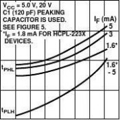
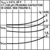
Very High CMR, Wide VCC LogicGate OptocouplersTechnical Data
HCPL-2201HCPL-2211HCPL-2231HCPL-0201HCNW2201
HCPL-2202HCPL-2212HCPL-2232HCPL-0211HCNW2211
Features
? 10 kV/μs Minimum CommonMode Rejection (CMR) atVCM = 1000 V
(HCPL-2211/2212/0211/2232, HCNW2211)
? Wide Operating VCC Range:4.5 to 20 Volts
? 300 ns Propagation DelayGuaranteed over the FullTemperature Range
? 5 Mbd Typical Signal Rate? Low Input Current (1.6mAto 1.8 mA)? Hysteresis
? Totem Pole Output (NoPullup Resistor Required)? Available in 8-Pin DIP,
SOIC-8, Widebody Packages? Guaranteed Performancefrom -40°C to 85°C? Safety Approval
UL Recognized -2500 V rmsfor 1 minute (5000V rmsfor 1 minute for
HCNW22XX) per UL1577CSA Approved
VDE 0884 Approved withVIORM= 630 V peak (HCPL-2211/2212 Option 060 only)and VIORM= 1414 V peak(HCNW22XX only)
BSI Certified (HCNW22XXonly)
? MIL-STD-1772 VersionAvailable
(HCPL-52XX/62XX)
Description
The HCPL-22XX, HCPL-02XX,and HCNW22XX are optically-coupled logic gates. The
HCPL-22XX, and HCPL-02XXcontain a GaAsP LED while theHCNW22XX contains an AlGaAsLED. The detectors have totempole output stages and opticalreceiver input stages with built-inSchmitt triggers to provide logic-compatible waveforms, eliminat-ing the need for additionalwaveshaping.
A superior internal shield on theHCPL-2211/12, HCPL-0211,
Applications
? Isolation of High SpeedLogic Systems
? Computer-PeripheralInterfaces
? Microprocessor SystemInterfaces
? Ground Loop Elimination? Pulse TransformerReplacement
? High Speed Line Receiver? Power Control Systems
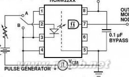
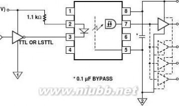
Functional Diagram
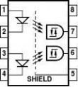
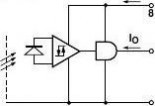
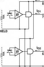
HCPL-2201/11??HCPL-0201/11??
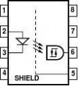
NCANODECATHODENCVCCVONCGND
NCANODECATHODENC
VCCNCVOGND
ANODE 1CATHODE 1CATHODE 2ANODE 2VCCVO1VO2GND
TRUTH TABLE??(POSITIVE LOGIC)LED??VO??ON??HIGH??OFFLOW
A 0.1 μF bypass capacitor must be connected between pins 5 and8.
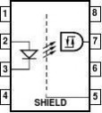
CAUTION: It is advised that normal static precautions be taken in handling and assembly of this component
to prevent damage and/or degradation which may be induced by ESD.5965-3595E
1-131
2211 HCNW-2211中文资料
元器件交易网www.cecb2b.com
HCPL-2232 and HCNW2211guarantees common mode
transient immunity of 10 kV/μs ata common mode voltage of 1000volts.
The electrical and switchingcharacteristics of the HCPL-22XX, HCPL-02XX and
HCNW22XX are guaranteed from-40°C to +85°C and a VCC from4.5 volts to 20 volts. Low IF and
Selection Guide


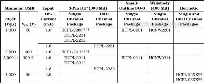
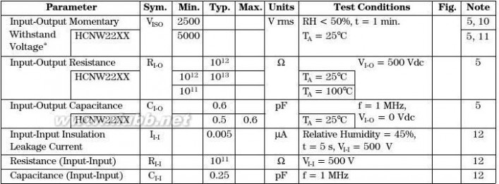
wide VCC range allow compatibil-ity with TTL, LSTTL, and CMOSlogic and result in lower powerconsumption compared to otherhigh speed couplers. Logic signalsare transmitted with a typicalpropagation delay of 150ns.
Notes:
1. HCPL-2200/2219 devices include output enable/disable function.
2. Technical data for the HCPL-2200/2219, HCPL-52XX and HCPL-62XX are on separate HP publications.3. Minimum CMR of 10 kV/μs with VCM = 1000 V can be achieved with input current, IF, of 5 mA.
Ordering Information
Specify Part Number followed by Option Number (if desired).Example:060 = VDE 0884 VIORM = 630 V peak Option*300 = Gull Wing Surface Mount Option**500 = Tape and Reel Packaging Option
Option data sheets available. Contact your Hewlett-Packard sales representative or authorized distributor forinformation.
*For HCPL-2211/2212 only.
**Gull wing surface mount option applies to through hole parts only.
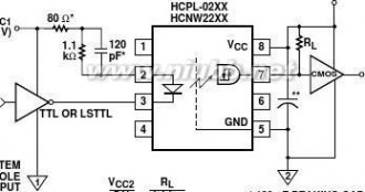
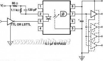
VCC
Schematic
VCC
VVO1
VO
HCPL-2201/02/11/12??HCPL-0201/11??HCNW2201/11
GND
VHCPL-2231/32
VO2
GND
1-132
2211 HCNW-2211中文资料
元器件交易网www.cecb2b.com
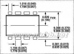
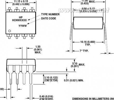
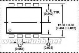
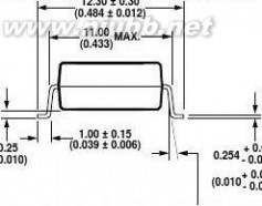
Package Outline Drawings
8-Pin DIP Package (HCPL-2201/02/11/12/31/32)
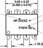
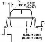
0.254+ 0.076- 0.051
扩展:hcnw3120中文资料 / msp430g2211中文资料 / hcnw4506
(0.010+ 0.003)- 0.002)
DIMENSIONS IN MILLIMETERS AND (INCHES).*MARKING CODE LETTER FOR OPTION NUMBERS"V" = OPTION 060
OPTION NUMBERS 300 AND 500 NOT MARKED.
8-Pin DIP Package with Gull Wing Surface Mount Option 300 (HCPL-2201/02/11/12/31/32)


+ 0.076??- 0.051
MAX.+ 0.003)??- 0.002)

(0.100)??
BSC
DIMENSIONS IN MILLIMETERS (INCHES).??
LEAD COPLANARITY = 0.10 mm (0.004 INCHES).
1-133
2211 HCNW-2211中文资料
元器件交易网www.cecb2b.com
Small-Outline SO-8 Package (HCPL-0201/11)
DIMENSIONS IN MILLIMETERS (INCHES).??
LEAD COPLANARITY = 0.10 mm (0.004 INCHES).MIN.(0.012)
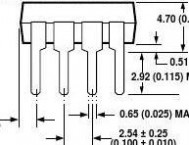
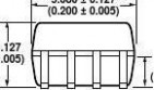
8-Pin Widebody DIP Package (HCNW2201/11)
+ 0.076??- 0.0051+ 0.003)??- 0.002)
1.78 ± 0.15??
1-134
2211 HCNW-2211中文资料
元器件交易网www.cecb2b.com
8-Pin Widebody DIP Package with Gull Wing Surface Mount Option 300 (HCNW2201/11)
MAX.1.78 ± 0.15??BSC
LEAD COPLANARITY = 0.10 mm (0.004 INCHES).
DIMENSIONS IN MILLIMETERS (INCHES).??
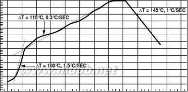
Solder Reflow Temperature Profile (HCPL-02XX and Gull Wing Surface Mount Option 300 Parts)

260240
220200180160140120100806040200
TEMPERATURE – °C
TIME – MINUTES
Note: Use of nonchlorine activated fluxes is highly recommended.
1-135
2211 HCNW-2211中文资料
元器件交易网www.cecb2b.com
Regulatory Information
The HCPL-22XX/02XX and
HCNW22XX have been approvedby the following organizations:UL
Recognized under UL 1577,Component RecognitionProgram, File E55361.
CSA
Approved under CSA ComponentAcceptance Notice #5, File CA88324.
VDE
Approved according to VDE0884/06.92. (HCPL-2211/2212Option 060 and HCNW22XX only)
BSI
Certification according toBS415:1994,
(BS EN60065:1994);BS EN60950:1992(BS7002:1992) and
EN41003:1993 for Class II
applications. (HCNW22XX only)
Insulation and Safety Related Specifications
8-pin DIP Package
8-Pin DIP (300 Mil)Value7.1
SO-8Value4.9
Widebody(400 Mil)ValueUnits9.6mm
Parameter Symbol
Minimum ExternalL(101)Air Gap (ExternalClearance)
Minimum ExternalL(102)Tracking (ExternalCreepage)
Minimum InternalPlastic Gap
(Internal Clearance)
7.44.810.0mm
0.080.081.0mm
Minimum InternalTracking (InternalCreepage)
Tracking Resistance(ComparativeTracking Index)Isolation Group
NANA4.0mm
CTI200200200Volts
Conditions
Measured from input terminalsto output terminals, shortestdistance through air.
Measured from input terminalsto output terminals, shortestdistance path along body.Through insulation distance,conductor to conductor, usuallythe direct distance between thephotoemitter and photodetectorinside the optocoupler cavity.Measured from input terminalsto output terminals, alonginternal cavity.
DIN IEC 112/VDE 0303 Part 1
IIIaIIIaIIIa
Material Group
(DIN VDE 0110, 1/89, Table 1)
Option 300 - surface mount classification is Class A in accordance with CECC 00802.
1-136
2211 HCNW-2211中文资料
元器件交易网www.cecb2b.com
VDE 0884 Insulation Related Characteristics(HCPL-2211/2212 Option 060 ONLY)
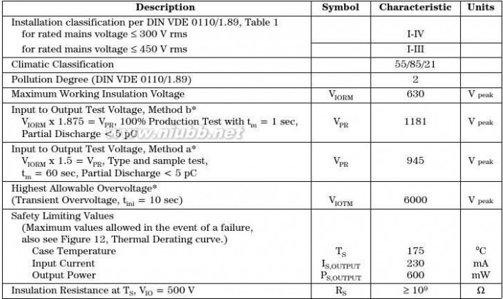
*Refer to the front of the optocoupler section of the current catalog, under Product Safety Regulations section (VDE 0884), for adetailed description.
扩展:hcnw3120中文资料 / msp430g2211中文资料 / hcnw4506
Note: Isolation characteristics are guaranteed only within the safety maximum ratings which must be ensured by protective circuits inapplication.
1-137
2211 HCNW-2211中文资料
元器件交易网www.cecb2b.com
VDE 0884 Insulation Related Characteristics (HCNW22XX ONLY)
*Refer to the front of the optocoupler section of the current catalog, under Product Safety Regulations section (VDE 0884), for adetailed description.
Note: Isolation characteristics are guaranteed only within the safety maximum ratings which must be ensured by protective circuits inapplication.
Absolute Maximum Ratings
1-138
2211 HCNW-2211中文资料
元器件交易网www.cecb2b.com
*The initial switching threshold is 1.6 mA or less. It is recommended that 2.2 mA be used to permit at least a 20% LED degradationguardband.
?The initial switching threshold is 1.8 mA or less. It is recommended that 2.5 mA be used to permit at least a 20% LED degradationguardband.
Electrical Specifications
-40°C ≤ TA ≤ 85°C, 4.5 V ≤ VCC ≤ 20 V, 1.6 mA ≤ IF(ON)* ≤ 5 mA, 0 V ≤ VF(OFF) ≤ 0.8 V, unless otherwisespecified. All Typicals at TA = 25°C. See Note 7.
*For HCPL-223X, 1.8 mA ≤ IF(ON) ≤ 5 mA.**Typical VOH = VCC - 2.1 V.
1-139
2211 HCNW-2211中文资料
元器件交易网www.cecb2b.com
Switching Specifications (AC)
-40°C ≤ TA ≤ 85°C, 4.5 V ≤ VCC ≤ 20 V, 1.6 mA ≤ IF(ON)* ≤ 5 mA, 0 V ≤ VF(OFF) ≤ 0.8 V.All Typicals at TA = 25°C, VCC = 5 V, IF(ON) = 3 mA unless otherwise specified.

*For HCPL-223X, 1.8 mA ≤ IF(ON) ≤ 5 mA.?IF = 1.8 mA for HCPL-2231.?IF = 1.8 mA for HCPL-2232.
1-140
2211 HCNW-2211中文资料
元器件交易网www.cecb2b.com
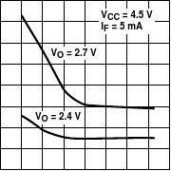
Package Characteristics
*The Input-Output Momentary Withstand Voltage is a dielectric voltage rating that should not be interpreted as an input-outputcontinuous voltage rating. For the continuous voltage rating refer to the VDE 0884 Insulation Characteristics Table (if applicable),your equipment level safety specification or HP Application Note 1074 entitled “Optocoupler Input-Output Endurance Voltage,”publication number 5963-2203E.
Notes:
1. Each channel.
2. Derate total package power dissipation, PT, linearly above 70°C free-air temperature at a rate of 4.5 mW/°C.3. Duration of output short circuit time should not exceed 10 ms.
4. For single devices, input capacitance is measured between pin 2 and pin 3.
5. Device considered a two-terminal device: pins 1, 2, 3, and 4 shorted together and pins 5, 6, 7, and 8 shorted together.
6. The tPLH propagation delay is measured from the 50% point on the leading edge of the input pulse to the 1.3 V point on theleading edge of the output pulse. The tPHL propagation delay is measured from the 50% point on the trailing edge of the inputpulse to the 1.3 V point on the trailing edge of the output pulse.
7. CMH is the maximum slew rate of the common mode voltage that can be sustained with the output voltage in the logic high state,VO > 2.0 V. CML is the maximum slew rate of the common mode voltage that can be sustained with the output voltage in the logiclow state, VO < 0.8 V.
8. For HCPL-2202/12, VO is on pin 6.
9. Use of a 0.1 μF bypass capacitor connected between pins 5 and 8 is recommended.
10. In accordance with UL 1577, each optocoupler is proof tested by applying an insulation test voltage ≥3000 V rms for one second
(leakage detection current limit, II-O ≤5 μA). This test is performed before the 100% production test for partial discharge (Methodb) shown in the VDE 0884 Insulation Characteristics Table, if applicable.
11. In accordance with UL 1577, each optocoupler is proof tested by applying an insulation test voltage ≥6000 V rms for one second
(leakage detection current limit, II-O ≤5 μA). This test is performed before the 100% production test for partial discharge (Methodb) shown in the VDE 0884 Insulation Characteristics Table.
12. For HCPL-2231/32 only. Measured between pins 1 and 2, shorted together, and pins 3 and 4, shorted together.
1-141
2211 HCNW-2211中文资料 扩展:hcnw3120中文资料 / msp430g2211中文资料 / hcnw4506
元器件交易网www.cecb2b.com
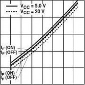
IOH – HIGH LEVEL OUTPUT CURRENT – mA
VOL – LOW LEVEL OUTPUT VOLTAGE – V
VO – OUTPUT VOLTAGE – V

-1-2-3-4-5-6-7
-8
TA – TEMPERATURE – °CTA – TEMPERATURE – °CIF – INPUT CURRENT – mA
Figure 1. Typical Logic Low OutputVoltage vs. Temperature.
HCPL-22XX??Figure 2. Typical Logic High OutputCurrent vs. Temperature.
Figure 3. Typical Output Voltage vs.Forward Input Current.
IF – FORWARD CURRENT – mA
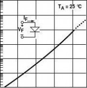
IF – FORWARD CURRENT – mA
VF – FORWARD VOLTAGE – VVF – FORWARD VOLTAGE – V
Figure 4. Typical Input Diode Forward Characteristic.
?
?
D2D3D4
D2D3D4
ARE INCLUDED IN C1 AND C2.2.15 k???1.10 k???681 ???R5 mAIF (ON)1.6 mA3 mA
ALL DIODES ARE 1N916 OR 1N3064.
ARE INCLUDED IN C1 AND C2.1.96 k???1.10 k???681 ???R5 mAIF (ON)1.8 mA3 mA
F (ON)VOL
ALL DIODES ARE 1N916 OR 1N3064.
Figure 5. Circuit for tPLH, tPHL, tr,tf.

* 0.1 μF BYPASS — SEE NOTE 9.
1-142
2211 HCNW-2211中文资料
元器件交易网www.cecb2b.com
250tP – PROPAGATION DELAY
– ns
HCPL-22XX??HCPL-02XX
PO – MAXIMUM OUTPUT POWERPER CHAN

NEL (mW)
tP – PROPAGATION DELAY – ns
200
250
200
150
150
100
100
50
50
TA – TEMPERATURE – °CTA – TEMPERATURE – °CVCC – SUPPLY VOLTAGE – V
Figure 6. Typical Propagation Delays vs. Temperature.
Figure 7. Maximum Output Power perChannel vs. Supply Voltage.
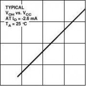
VOH – HIGH LEVE
L OUTPUT VOLTAGE – V
20
tr, tf – RISE, FALL
TIME – ns
15
10
5
VCC – SUPPLY VOLTAGE – VTA – TEMPERATURE – °C
Figure 8. Typical Logic High OutputVoltage vs. Supply Voltage.Figure 9. Typical Rise, Fall Time vs.Temperature.
HCPL-2201/11??HCPL-02XX??OOR
VFF
VFF
|VCM|
VCM (PEAK)
0 V
SWITCH AT A: I = 1.6 mA**VO (MIN.)*
SWITCH AT B: VF = 0 V
VO (MAX.)*
VOH
OUTPUT VO
VOL
* SEE NOTE 7, 9.??
** IF = 1.8 mA FOR HCPL-2231/32 DEVICES.
Figure 10. Test Circuit for Common Mode Transient Immunity and Typical Waveforms.
1-143
2211 HCNW-2211中文资料
元器件交易网www.cecb2b.com
1.0
INPUT CURRENT THRESHOLD – mAHCPL-22XX??INPUT CURRENT THRESHOLD – mAHCNW22XX0.90.8
0.70.60.5

TA – TEMPERATURE – °CTA – TEMPERATURE – °C
Figure 11. Typical Input Threshold Current vs. Temperature.
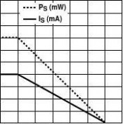
OUTPUT POWER – PS, INPUT CURRENT – IS
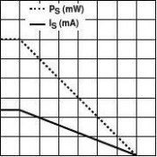
8007006005004003002001000OUTPUT POWER PS, INPUT CURRENT IS10009008007006005004003002001000HCNW22XXTS – CASE TEMPERATURE – °CTS – CASE TEMPERATURE – °C
Figure 12. Thermal Derating Curve, Dependence of Safety Limiting Value withCase Temperature per VDE 0884.
HCPL-2201/11??
HCPL-02XX??
VCC1
DATA INPUT
VCC2 (+5 V)DATA OUTPUTUP TO 16 LSTTL LOADS??
OR 4 TTL LOADS
扩展:hcnw3120中文资料 / msp430g2211中文资料 / hcnw4506
Figure 13a. Recommended LSTTL to LSTTL Circuit where 500 ns PropagationDelay is Sufficient.
1-144
2211 HCNW-2211中文资料
元器件交易网www.cecb2b.com
HCPL-2201/11??HCPL-02XX??VCC1 DATA INPUT
VCC2 (+5 V)
DATA OUTPUT
UP TO 16 LSTTL LOADS??OR 4 TTL LOADS
Figure 13b. Recommended LSTTL to LSTTL Circuit for Applications Requiringa Maximum Allowable Propagation Delay of 300 ns.
VVCC2 ??DATA??OUTPUT
DATA??INPUT
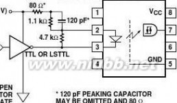
VCC1HCPL-2201/11??HCPL-02XX??10 V??15 V??20 V2.37 k?3.83 k?5.11 k?
MAY BE OMITTED AND 80 ?RESISTOR MAY BE SHORTED??WHERE 500 ns PROPAGATION??DELAY IS SUFFICIENT.**0.1 μF BYPASS
Figure 14. LSTTL to CMOS Interface Circuit.
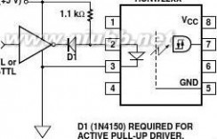
Figure 15. Alternative LED DriveCircuit.
HCPL-2201/11??HCPL-02XX??VCC DATA INPUT
RESISTOR MAY BE SHORTED??WHERE 500 ns PROPAGATION??DELAY IS SUFFICIENT.
Figure 16. Series LED Drive with Open Collector Gate(4.7k Resistor Shunts IOH from the LED).
1-145
扩展:hcnw3120中文资料 / msp430g2211中文资料 / hcnw4506
三 : 4066中文资料
CD4066中文资料
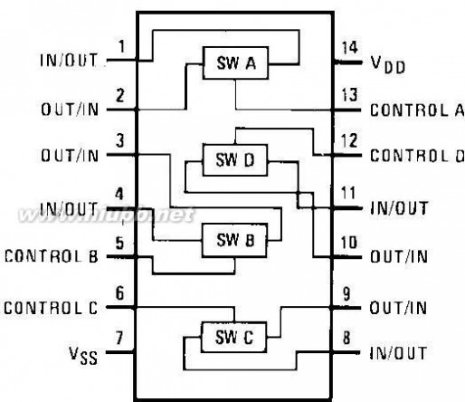
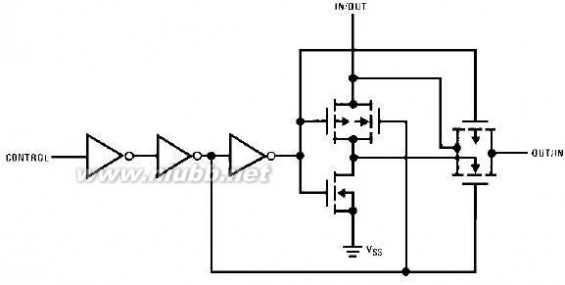
CD4066 的引脚功能下图所示。(www.61k.com]每个封装内部有4 个独立的模拟开关,每个模拟开关有输入、输出、控制三个端子,其中输入端和输出端可互换。当控制端加高电平时,开关导通;当控制端加低电平时开关截止。模拟开关导通时,导通电阻为几十欧姆;模拟开关截止时,呈现很高的阻抗,可以看成为开路。模拟开关可传输数字信号和模拟信号,可传输的模拟信号的上限频率为40MHz。各开关间的串扰很小,典型值为-50dB。
CD4066是四双向模拟开关,主要用作模拟或数字信号的多路传输。CD4066由四个相互独立的双向开关组成,每个开关有一个控制信号端,开关可以相互独立地开断,互补影响。这种结构消除了开关晶体管阈值电压随输入信号的变化,因此在整个工作信号范围内导通阻抗比较低。CD4066引出端排列与CC4016一致,但具有比较低的导通阻抗。另外,导通阻抗在整个输入信号范围内基本不变。与单通道开关相比,具有输入信号峰值电压范围等于电源电压以及在输入信号范围内导通阻抗比较稳定等优点。但若应用于采保电路,仍推荐CD4016。
当模拟开关的电源电压采用双电源时,例如 =﹢5V, =﹣5V(均对地0V而言),则输入电压对称于0V的正、负信号电压(﹢5V~﹣5V)均能传输。这时要求控制信号C=“1”为+5V,C=“0”为-5V,否则只能传输正极性的信号电压。
CD4066功能图
cd4066 4066中文资料
内部方框图
Absolute Maximum Ratings 绝对最大额定值:
Supply Voltage电源电压(VDD) ?0.5V to +18V
Input Voltage输入电压 (VIN) ?0.5V to VCC+0.5V
Storage Temperature Range储存温度?65℃ to +150℃ 范围 (TS)
Power Dissipation功耗 (PD)
Dual-In-Line 普通双列封装 700 mW
Small Outline 小外形封装 500 mW
Lead Temperature 焊接温度(TL)
Soldering, 10 seconds)(焊接10秒) 300℃
Recommended Operating Conditions 建议操作条件:
Supply Voltage电源电压(VDD) 3V to 15V
Input Voltage输入电压 (VIN) 0V to VDD
Operating Temperature Range工作温度范围 ?55℃ to +125℃ (TA)
DC Electrical Characteristics 直流电气特性:
?55℃ +25℃ +125℃ SymParameter 参Conditions 条件 最最最典最最最bol 数 符号 小 大 小 型 大 小 大
0.0.00.2VDD = 5V 7.5 25 1 5 Quiescent 0.0.0IDD Device CurrentVDD = 10V 0.5 15 5 1 静态电流 1.0.0VDD = 15V 1.0 30 0 1
SIGNAL INPUTS AND OUTPUTS
RON “ON” RL = 10 kΩ to (VDD ? VSS/2) VC = VDD, VSS to VDD Units 单位 μA
cd4066 4066中文资料
Resistance
VDD = 5V VDD = 10V VDD = 15V
800 310 200 ±50
270 120 80
1050 400 240
1300 550 320
Ω
Δ“ON”
ΔRON
Resistance Between Any 2 of 4 Switches Input or Output
IIS
RL = 10kΩ to (VDD ? VSS/2) VCC = VDD, VIS = VSS to VDD VDD = 10V VDD = 15V
10 5 ±0.1
Ω
Leakage Switch VC = 0 “OFF”
±50 ±500 nA
CONTROL INPUTS
VIS = V SS and VDD VOS = V DD and VSS IIS = ± 10μA
LOW
VILC
Input 压
VDD = 15V VDD = 5V
HIGH
VIHC
Input 压
Level Voltage
VDD=10V (Note 7) VDD = 15V
Level VDD = 5V Voltage
VDD = 10V
1.5 3.0 4.0
3.5
2.25 4.5 6.75 2.75
1.5 3.0 4.0
3.5 7.0 1 ?0.1
1.0
?0.1
μA
0.1 1.5 3.0 4.0
V
输入低电平电
3.5 7.0 11.0
7.0 5.5 11.0
8.25 ?10
?5
输入高电平电
V
?0.1 0.1
IIN
Input Current
VDD?VSS = 15V VDD≥VIS≥VSS VDD≥VC≥VSS
输入电流
10?5 0.1
AC Electrical Characteristics 交流电气特性: Symbol 符号
VC = VDD, CL = 50 pF, (Figure 1)RL = 200k
Propagation Delay
tPHL,
Time Signal Input to Signal Output信传递延迟时间
VDD = 5V VDD = 10V VDD = 15V
25 15 10
55 35 25
ns
Parameter 参数
Conditions 条件
最
典最
Units 单位
小 型 大
tPLH 号输入到信号输出
cd4066 4066中文资料
RL = 1.0kΩ, CL = 50pF, (Figure 2, Figure 3)
Propagation Delay
tPZH,
Time Control Input to Signal Output
1
VDD = 5V
25 6ns
tPZL High Impedance to VDD = 10V
Logical Level
Propagation Delay
Time Control Input to Signal Output Logical Level to High Impedance
Sine Wave
Distortion Frequency Response-Switch “ON” (Frequency at ?3 dB)
tPHZ,
tPLZ Feedthrough
— Switch “OFF” (Frequency at ?50
dB) Crosstalk
Between Any Two Switches (Frequency at ?50 dB) Crosstalk;
Control Input to Signal Output Maximum Control
Input
Signal
Input
CIS
Capacitance信号输入电容 Signal
Output
COS
Capacitance信号
输出电容
0 VDD = 15V
50
RL = 1.0kΩ, CL = 50pF
1VDD = 5V
25 VDD = 10V 60 VDD = 15V
50 VC = VDD = 5V, VSS = ?5V RL = 10 kΩ, VIS = 5Vp-p, f= 1 kHz, (Figure 4)
0.1
VC = VDD = 5V, VSS = ?5V, RL = 1 kΩ,
VIS = 5Vp-p, 20 Log10 VOS/VOS (1 40 kHz)?dB,(Figure 4)
VDD = 5.0V, VCC = VSS = ?5.0V, RL = 1 1.kΩ, VIS = 5.0Vp-p, 20 Log10, VOS/VIS = 2
?50 dB, (Figure 4)
5 VDD=VC(A) =5.0V; VSS = VC(B) = 5.0V, RL1kΩ, VIS(A) = 5.0Vp-p, 20 Log10, 0.VOS(B)/VIS(A) = ?50dB (Figure 5)
9
VDD
=10V,RL=10kΩ,
RIN=1.0kΩ,VCC=10V Square Wave, CL
1=50pF(Figure 6) 5
0 RL=1.0kΩ, CL=50pF, (Figure 7)VOS(f) = ? VOS(1.0 kHz)
VDD = 5.0V
6.0 VDD = 10V 8.0 VDD = 15V
8.5
8.0 VDD = 10V
8.0
ns % MHz
MHz mVp-pMHz
pF
pF
cd4066 4066中文资料
CIO
S Feedthrough Capacitance馈电
容
Control Input
Capacitance控制
输入电容 VC = 0V 0.5 5.0 pF CIN 7.
5 pF
应用举例:
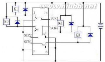
CD4066是四双向模拟开关驱动继电器应用电路
CD4066是四双向模拟开关,集成块SCR1~SCR4为控制端,用于控制四双向模拟开关的通断。[www.61k.com)当SCR1接高电平时,集成块①、②脚导通,+12V→K1→集成块①、②脚→电源负极使K1吸合;反之当SCR1输入低电平时,集成块①、②脚开路,K1失电释放,SCR2~SCR4输入高电平或低电平时状态与SCR1相同。
四 : MJE13003中文资料
元器件交易网www.cecb2b.com
MJE13003
FEATURES
Power dissipation
PCM : 1.25 W


Collector current
ICM : 1.5 A Collector-base voltage V(BR)CBO : 700 V


Tamb=25
ELECTRICAL CHARACTERISTICS
Parameter
Collector-base breakdown voltageCollector-emitter breakdown voltageEmitter-base breakdown voltageCollector cut-off currentCollector cut-off currentEmitter cut-off current
Tamb=25
SymbolV(BR)CBOV(BR)CEOV(BR)EBO ICBO ICEO IEBOHFE
1
unless otherwise specified
Test conditionsIc= 1000
A IE=0
MIN7004009
1000500
1000
85
11.23
5
0.52.5
VVVMHzμsμs
40
TYP
MAX
UNITVVVμAμAμA
Ic= 10 mA IB=0IE= 1000
A IC=0
VCB= 700 V IE=0VCE= 400 V IB=0VEB

= 9 V IC=0VCE= 10 V, IC= 150 mAVCE= 10 V, IC= 0.5 mAIC=1000mA,IB= 250 mAIC=1000mA, IB= 250mAIE= 2000 mAVCE=10V,Ic=100mA
f =1MHz
IC=1A, IB1=-IB2=0.2AVCC=100V
DC current gain(note)
HFE
Collector-emitter saturation voltageBase-emitter saturation voltageBase-emitter voltageTransition frequencyFall timeStorage time
2
VCE(sat)VBE(sat)VBEfTtfts
CLASSIFICATION OF HFE(1)
RankRange
8-15
15-20
20-25
25-30
30-35
35-40
Wing Shing Computer Components Co., (H.K.)Ltd.Homepage:http://www.wingshing.comTel:(852)2341 9276 Fax:(852)2797 8153E-mail: wsccltd@hkstar.com
扩展:mje13003 / mje13003参数 / mje13003三极管参数
本文标题:中文资料-TPS2552-1中文资料61阅读| 精彩专题| 最新文章| 热门文章| 苏ICP备13036349号-1