一 : IAQ中文资料
空气质量传感器模块
IAQ2000
正常人每天要消耗两三升水和一到两公斤的食物,食品安全和卫生得到了极大重视的同时,空气质量却没有获得足够关注,尽管我们每天吸入15千克的空气——80%是在室内。
从教室到卧室,维持良好的空气质量就是在保障居民的健康。在健康的空气中上课的学生更容易记住所学知识,老师也更少请病假。对于雇主,研究表明,改善室内空气质量的好坏直接与更高的生产力和更高的员工满意度密切相关。此外,“绿色建筑”和有关排放的能源税的推出使得大家意识到室内空气质量及通风能耗的重要性。。而在现代建筑中,通风不足造成空气质量变差及永久通风换气的高耗能是相矛盾的,两者之间就需要通过“需求控制通风”即DCV系统达到平衡。
本文主要阐述的是“需求控制通风”系统所采用的空气质量传感器。主要说明一般的室内空气污染物、来源以及它们对人类健康的影响。此外,针对当前的需求与现代通风室内空气质量标准,同现有市场上的商用空气质量传感器技术进行比较。最后,通过典型案例提出采用德国IAQ传感器的解决方案。
室内空气剖析
清洁的空气是由21%的氧气,78%的氮气和1%的氩气组成。不过室内环境还存在其他一些微量气体:一氧化碳(CO),二氧化碳(CO2)和有机挥发物(VOC)等,危及人体健康的气体后两者是最重要的,二氧化碳气体已经是HVAC暖通空调行业认可的标准,VOC则是由于其危害性。
IntelligentAirQuality…BeyondCO2?1
…beyondCO
室内空气中VOC的作用和影响2
据估计,世界上共有5000到10000种不同的VOC,室内空气中的种类是室外的约2到5倍,室内的VOC主要是碳氢化合物,有两个主要来源:生物废水(包括人体呼吸,蒸发和新陈代谢等)及来自建筑材料和家具产生的蒸汽。挥发性有机物VOC会引起眼睛不适,头痛,嗜睡或头晕,并容易导致“室内空气综合症”,因此,必须保证充分的通风。除了保证舒适性如温度控制而保持通风外,挥发性有机化合物VOC是通风更重要的原因。一些典型的室内污染物及其来源见表1。显然,人类是VOC直接和间接的最大来源;远远超出建材,家具和办公设备,从而在通风需求中占据首要地位。

IntelligentAirQuality…BeyondCO2?2

室内空气中CO2的作用和影响
尽管二氧化碳气体在表1中提到了两次,并且
在现代通风控制中起了主要作用,但是如果是少量
的二氧化碳,对人类没有长时间的影响。据潜艇和
国际空间站证实,即使1%(10,000ppm)浓度的CO2
对空间站内的人员健康也不会造成不可逆转的
影响。一直以来,由于缺少适合探测VOC的感应
器件,二氧化碳的含量曾是历史上唯一衡量空气
质量的指标,但是,由于人类呼吸和散发(代谢
规律)而产生的二氧化碳含量和VOCs含量是
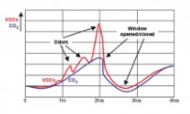
成正比的,所以二氧化碳的浓度也间接反映出了图1:商业会议中心监测的CO2和VOCs曲线图因此二氧化碳气体作为一种容易又单一的目标分析物和成千上万
的VOCS相比,再结合已经成熟的适合测量CO2浓度的技术,
已经让CO2气体作为室内空气污染环境检测判断的替代物质。
这样CO2浓度才作为如今的需求控制通风DCV判断室内空气质
量的参考标准,这个标准最初由MaxvonPettenkofer先生引
入,并且做为大多数的HVAC工业标准。请参考见表2
挥发性有机化合物的不稳定性
图1不仅仅说明了VOCs和CO2之间的相关性,更重要的是,
图中也说明了VOCS气体具有更的的不稳定性和突变性。人
类不断增加的生活废水及间断的使用芳香类的物质,例如:
清洁用品,香水或者香烟都是很常见的。图1中显示了这些物
表2-室内空气质量分类质的峰值变化,因此,仅仅依靠CO2浓度作为通风的依据,并不能得到满意的结果。通风系统需要对所有的污染气体做出反应,而不仅仅是CO2。这也突出了传统的基于减少对居住者的影响。
IntelligentAirQuality…BeyondCO2CO2浓度的需要控制通风DCV系统的弱点,检测更大范围的污染物质,能够优化通风节能,并且最大限度的?3
从过去到现在的室内空气质量参考标准
历史上,CO2浓度由于其合理的参照及容易检测而用以做为室内空气质量的参考标准。而混合气体或VOC的检测因其长期稳定性的问题和无法校准等而遭受了一些非议。此外,由于没有合适的临界值,采用VOC检测的HVAC设计师不容易设置通风量,并且VOC传感器的漂移性致使整个通风系统功能不可预测。尽管测量空气污染的根源的动机是正确的,但并没有实施成功。
通过需求控制通风DCV系统节省什么?
可以有多种措施达致通风节能的要求。通风系统可以保持恒定的空气流量持续动作-----CAV,变风量统计---VAV,以及需求控制通风----DCV,而DCV又有多种控制选择:温度,CO2,VOC,湿度控制,这四种是目前常用的参看变量。
安装在空气处理机组的IAQ传感器比定时通风控制器节约了24%的运行时间,这减少了 在健身中心进行的测试数据表明
60%的能量损耗。到健身房中心的顾客对空气质量的改善表示赞赏。
采用德国AS公司IAQ技术的需求控制通风DCV系统意味着以最低的成本达致优良的室内空气质量和居民的健康
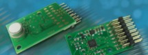
气候监控一般是通过温湿度、二氧化碳浓度等参数来评估室内的空气质量的,不过对用户来说,评估空气质量主要参考的是VOC的含量,如香烟,烹饪的气味,生物挥发物及室外的污染物来判断的。二氧化碳传感器模块IAQ2000是一款高灵敏度,低成本的二氧化碳空气质量传感器模块。二氧化碳传感器模块IAQ2000更接近人体对空气质量的感知,加之小尺寸,低功耗,适宜于多种场合。 空气质量传感器模块(CO2浓度)的详细介绍 空气质量二氧化碳传感器模块 主要特点: 同CO2水平紧密相关,相当于450ppm-2000ppm CO2浓度 高灵敏度,快速响应 小尺寸,方便安装 低功耗(30mA) 自动零点校准 输出:I2C,PWM,0-5V
测量物质: 酒精, 醛类气体, 脂肪族烃,有机胺类,芳香烃,酮类,有机酸,CO, CH4,LPG等
应用:适合于所有环境(汽车,办公室,学校,厨房,浴室,车间等)空气质量监测; 专业的HVAC设备,包括空气净化机,中央空调,空气清新机等
IntelligentAirQuality…BeyondCO2?4


IAQ2000的解决方式-接近人类的知觉
考虑到缺少VOC的参考标准,德国AS公司的IAQ2000传感器采取了逆新陈代谢规则RMR技术。RMR技术可以校准要测量的VOC浓度同CO2等同于ppm的浓度值对应,,这样就实现了同CO2标准的完全兼容。此外,IAQ传感器还可以捕捉到的所有VOC气体排放,而在CO2传感器是无法检测到的,就像图2所示的。更重要的是,德国AS公司IAQ2000的控制算法能够校正传感器的漂移和老化,进而保证了工作的一致性。IAQ传感器通过检测通风需求的根本原因—VOC气体而克服了CO2检测的缺陷,此外,通过信号保持建立同CO2标准的关系及严格的漂移补偿技术延长了传感器寿命而弥补了传统的VOC传感器的不足。IAQ传感器模拟人体对空气质量的感知,甚至可以探测无味的潜在的有毒物质,例如一氧化碳气体。
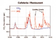
图2-二氧化碳传感器对挥发性有机化合物完全失效的典型案例参考
到底参考什么标准
如今,市场上有各种各样的需求控制通风DCV传感器,包括进入探测,CO2探测,湿度测量,VOC感应等。表3给出了后三种空气品质传感器在各种应用环境中的性能,很清晰的显示出了德国AS公司IAQ2000公司的IAQ技术优势。
表3-各种空气品质传感器在典型的通风方案中的比较
何时和如何通风
答案是:根据需要而定。大多数VOC气体活动是不可预测的,因为他们取决于人类的新陈代谢和行为,这在所有的通风案件中占85%的比例。其余的来自新的建筑或刚翻新的建筑中建筑材料或家具及涂料的排放。要充分的削弱这些排放的影响,低速率的持续的保持最大通风量的5-10%就足够了。表1列出了有关的污染气体并相应建议的通风条件。VOC的排放很少单独发生,因此,两者通风类型的组合是理想的解决方案。
IntelligentAirQuality…BeyondCO2?

5


IAQ的多种应用
装配了德国AS公司的IAQ2000传感器后,就有很多机会改善室内空气质量,并且降低DCV系统的能耗。以下是这些应用的图示。
IAQ-集成壁挂式空气质量记录仪
中央空气质量(AHU)或楼宇自动化系统
IAQ-集成管道安装空气质量记录仪中央空气质量(AHU)或楼宇自动化系统(BAS)进气/排气阀门的控制
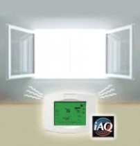
分散通风系统浴室/卧室通风系统独立空气处理单元墙壁控制窗户自动通风空气质量指示器提供手动换气建议开/关窗户空气清新机
IntelligentAirQuality…BeyondCO2?6
二 : 93C86中文资料
元器件交易网www.cecb2b.com
93C76/86
8K/16K 5.0V Microwire? Serial EEPROM
FEATURES
?Single 5.0V supply
?Low power CMOS technology-1 mA active current typical
?ORG pin selectable memory con?guration1024 x 8- or 512 x 16-bit organization (93C76)2048 x 8- or 1024 x 16-bit organization (93C86)?Self-timed ERASE and WRITE cycles(including auto-erase)
?Automatic ERAL before WRAL
?Power on/off data protection circuitry?Industry standard 3-wire serial I/O
?Device status signal during ERASE/WRITE cycles?Sequential READ function
?10,000,000 ERASE/WRITE cycles guaranteed?Data retention > 200 years?8-pin PDIP/SOIC package
?Temperature ranges supported-Commercial (C):0°Cto+70°C-Industrial-40°Cto+85°C-Automotive (E)-40°Cto +125°C
DESCRIPTION
The Microchip Technology Inc. 93C76/86 are 8K and16K low voltage serial Electrically Erasable PROMs.The device memory is con?gured as x8 or x16 bitsdepending on the ORG pin setup. Advanced CMOStechnology makes these devices ideal for low powernon-volatile memory applications. These devices alsohave a Program Enable (PE) pin to allow the user towrite protect the entire contents of the memory array.The 93C76/86 is available in standard 8-pin DIP and 8-pin surface mount SOIC packages.
Microwire is a registered trademark of National Semiconductor Incorporated.
? 1996 Microchip Technology Inc.
Preliminary
ThisdocumentwascreatedwithFrameMaker404
DS21132C-page 1
86中文 93C86中文资料
元器件交易网www.cecb2b.com
93C76/86
1.0
1.1
ELECTRICAL
CHARACTERISTICS
1.2AC Waveform:
VLO = 2.0VVHI = Vcc - 0.2VVHI = 4.0V for
(Note 1)(Note 2)
VCC...................................................................................7.0VAll inputs and outputs w.r.t. VSS ...............-0.6V to Vcc +1.0VStorage temperature.....................................-65?C to +150?CAmbient temp. with power applied.................-65?C to +125?CSoldering temperature of leads (10 seconds).............+300?CESD protection on all pins................................................4 kV
*Notice: Stresses above those listed under “Maximum ratings”may cause permanent damage to the device. This is a stress rat-ing only and functional operation of the device at those or anyother conditions above those indicated in the operational listingsof this speci?cation is not implied. Exposure to maximum ratingconditions for extended periods may affect device reliability
Timing Measurement Reference Level
InputOutput
Note 1:For VCC ≤ 4.0V
2:For VCC > 4.0V
0.5 VCC0.5 VCC
TABLE 1-1:
NameCSCLKDIDOVSSORGPEVCC
PIN FUNCTION TABLE
Function
Chip Select
Serial Data ClockSerial Data InputSerial Data OutputGround
Memory Con?gurationProgram EnablePower Supply
TABLE 1-2:DC CHARACTERISTICS
Applicable over recommended operating ranges shown below unless otherwise noted:VCC = +4.5V to +5.5VCommercial (C):Tamb = 0°C to -40°CIndustrial (I):Tamb = -40°C to +85°CAutomotive (E):Tamb = -40°C to +125°CParameter
High level input voltageLow level input voltageLow level output voltageHigh level output voltageInput leakage currentOutput leakage currentPin capacitance(all inputs/outputs)Operating current
SymbolVIH1VIL1VOL1VOL2VOH1VOH2ILIILOCINT
Min.2.0-0.3——2.4VCC-0.2-10-10—
Max.VCC +10.80.40.2——10107
UnitsVVVVVVμAμApF
Conditions
——
IOL = 2.1 mA; VCC = 4.5VIOL =100 μA; VCC = 4.5VIOH = -400 μA; VCC = 4.5VIOH = -100 μA; VCC = 4.5V.VIN = 0.1V to VCCVOUT = 0.1V to VCC
(Note Note:)
Tamb = +25?C, FCLK = 1 MHz FCLK = 2 MHz; VCC = 5.5VFCLK = 2 MHz; VCC = 5.5VCLK = CS = 0V; VCC = 5.5V
ICC write—3mAICC read—1.5mA
Standby currentICCS—100μANote:This parameter is periodically sampled and not 100% tested.
DS21132C-page 2
Preliminary
? 1996 Microchip Technology Inc.
86中文 93C86中文资料
元器件交易网www.cecb2b.com
93C76/86
TABLE 1-3:
AC CHARACTERISTICS
Applicable over recommended operating ranges shown below unless otherwise noted:VCC = +4.5V to +5.5VCommercial (C):Tamb = 0°C to -40°CIndustrial (I):Tamb = -40°C to +85°CAutomotive (E):Tamb = -40°C to +125°CParameter
Clock frequencyClock high timeClock low time
Chip select setup timeChip select hold timeChip select low timeData input setup timeData input hold timeData output delay timeData output disable timeStatus valid timeProgram cycle time
SymbolFCLKTCKHTCKLTCSSTCSHTCSLTDISTDIHTPDTCZTSVTWCTECTWL—
Min.—300200500250100100——————10M
Max.2———————400100500101530—
UnitsMHznsnsnsnsnsnsnsnsnsnsmsmsmscycles
ConditionsVcc ≥ 4.5V
Relative to CLKRelative to CLKRelative to CLKRelative to CLKCL = 100 pF(Note 1)
CL = 100 pF
ERASE/WRITE mode (Note 2)ERAL modeWRAL mode
25°C, VCC = 5.0V, Block Mode(Note 3)
Endurance
Note 1:This parameter is periodically sampled and not 100% tested.
2:Typical program cycle is 4 ms per word.
3:This parameter is not tested but guaranteed by characterization. For endurance estimates in a speci?c appli-cation, please consult the Total Endurance Model which can be obtained on our BBS or website.
TABLE 1-4:
InstructionREADEWENERASEERALWRITEWRALEWDS
INSTRUCTION SET FOR 93C76: ORG=1 (X16 ORGANIZATION)
SB1111111
Opcode10001100010000
Address
X A8 A7 A6 A5 A4 A3 A2 A1 A01 1 X X X X X X X XX A8 A7 A6 A5 A4 A3 A2 A1 A01 0 X X X X X X X XX A8 A7 A6 A5 A4 A3 A2 A1 A00 1 X X X X X X X X0 0 X X X X X X X X
Data In ————D15 - D0D15 - D0—
Data OutD15 - D0High-Z(RDY/BSY)(RDY/BSY)(RDY/BSY)(RDY/BSY)High-Z
Req. CLK Cycles
29131313292913
TABLE 1-5:
InstructionREADEWENERASEERALWRITEWRALEWDS
INSTRUCTION SET FOR 93C76: ORG=0 (X8 ORGANIZATION)
SB1111111
Opcode10001100010000
Address
X A9 A8 A7 A6 A5 A4 A3 A2 A1 A01 1 X X X X X X X X X X A9 A8 A7 A6 A5 A4 A3 A2 A1 A01 0 X X X X X X X X X X A9 A8 A7 A6 A5 A4 A3 A2 A1 A00 1 X X X X X X X X X0 0 X X X X X X X X X
Data In ————D7 - D0D7 - D0—
Data OutD7 - D0High-Z(RDY/BSY)(RDY/BSY)(RDY/BSY)(RDY/BSY)High-Z
Req. CLK Cycles
22141414222214
? 1996 Microchip Technology Inc.
Preliminary
DS21132C-page 3
86中文 93C86中文资料
元器件交易网www.cecb2b.com
93C76/86
TABLE 1-6:
InstructionREADEWENERASEERALWRITEWRALEWDS
INSTRUCTION SET FOR 93C86: ORG=1 (X16 ORGANIZATION)
SB1111111
Opcode10001100010000
Address
A9 A8 A7 A6 A5 A4 A3 A2 A1 A01 1 X X X X X X X X A9 A8 A7 A6 A5 A4 A3 A2 A1 A01 0 X X X X X X X XA9 A8 A7 A6 A5 A4 A3 A2 A1 A00 1 X X X X X X X X0 0 X X X X X X X X
Data In ————D15 - D0D15 - D0—
Data OutD15 - D0High-Z(RDY/BSY)(RDY/BSY)(RDY/BSY)(RDY/BSY)High-Z
Req. CLK Cycles
29131313292913
TABLE 1-7:
InstructionREADEWENERASEERALWRITEWRALEWDS
INSTRUCTION SET FOR 93C86: ORG=0 (X8 ORGANIZATION)
SB1111111
Opcode10001100010000
Address
A10 A9 A8 A7 A6 A5 A4 A3 A2 A1 A01 1 X X X X X X X X XA10 A9 A8 A7 A6 A5 A4 A3 A2 A1 A01 0 X X X X X X X X XA10 A9 A8 A7 A6 A5 A4 A3 A2 A1 A00 1 X X X X X X X X X0 0 X X X X X X X X X
Data In
Data Out
Req. CLK Cycles
22141414222214
—D7 - D0—High-Z—(RDY/BSY)—(RDY/BSY)D7 - D0(RDY/BSY)D7 - D0(RDY/BSY)—High-Z
DS21132C-page 4
Preliminary
? 1996 Microchip Technology Inc.
86中文 93C86中文资料
元器件交易网www.cecb2b.com
93C76/86
2.0
PRINCIPLES OF OPERATION
When the ORG pin is connected to VCC, the x16 orga-nization is selected. When it is connected to ground, thex8 organization is selected. Instructions, addressesand write data are clocked into the DI pin on the risingedge of the clock (CLK). The DO pin is normally held ina high-Z state except when reading data from thetus can be veri?ed during an Erase/Write operation bypolling the DO pin; DO low indicates that programmingis still in progress, while DO high indicates the device isready. The DO will enter the high impedance state onthe falling edge of the CS.
low all programming operations. Execution of a READinstruction is independent of both the EWEN andEWDS instructions.
2.4During power-up, all programming modes of operationare inhibited until VCC has reached a level greater than1.4V. During power-down, the source data protectioncircuitry acts to inhibit all programming modes whenVCC has fallen below 1.4V.
The EWEN and EWDS commands give additional pro-tection against accidentally programming during nor-mal operation.
After power-up, the device is automatically in theEWDS mode. Therefore, an EWEN instruction must beperformed before any ERASE or WRITE instruction canbe executed.
2.1The START bit is detected by the device if CS and DIare both HIGH with respect to the positive edge of CLKfor the ?rst time.
Before a START condition is detected, CS, CLK, and DImay change in any combination (except to that of aSTART condition), without resulting in any device oper-ation (READ, WRITE, ERASE, EWEN, EWDS, ERAL,and WRAL). As soon as CS is HIGH, the device is nolonger in the standby mode.
An instruction following a START condition will only beexecuted if the required amount of opcode, addressand data bits for any particular instruction are clockedin.
After execution of an instruction (i.e., clock in or out ofthe last required address or data bit) CLK and DIbecome don't care bits until a new start condition isdetected.
2.2It is possible to connect the Data In and Data Out pinstogether. However, with this con?guration it is possiblefor a “bus con?ict” to occur during the “dummy zero” thatprecedes the READ operation, if A0 is a logic HIGHlevel. Under such a condition the voltage level seen atData Out is unde?ned and will depend upon the relativeimpedances of Data Out and the signal source drivingA0. The higher the current sourcing capability of A0, thehigher the voltage at the Data Out pin.
2.3
The 93C76/86 powers up in the Erase/Write Disable(EWDS) state. All programming modes must be pre-ceded by an Erase/Write Enable (EWEN) instruction.Once the EWEN instruction is executed, programmingremains enabled until an EWDS instruction is executedor VCC is removed from the device. To protect againstaccidental data disturb, the EWDS instruction can beused to disable all Erase/Write functions and should fol-
? 1996 Microchip Technology Inc.
Preliminary
DS21132C-page 5
86中文 93C86中文资料
元器件交易网www.cecb2b.com
93C76/86
3.0
3.1
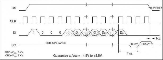
DEVICE OPERATION
The READ instruction outputs the serial data of theaddressed memory location on the DO pin. A dummyzero bit precedes the 16 bit (x16 organization) or 8 bit(x8 organization) output string. The output data bits willtoggle on the rising edge of the CLK and are stable afterthe speci?ed time delay (TPD). Sequential read is pos-sible when CS is held high and clock transitions con-tinue. The memory address pointer will automaticallyincrement and output data sequentially.
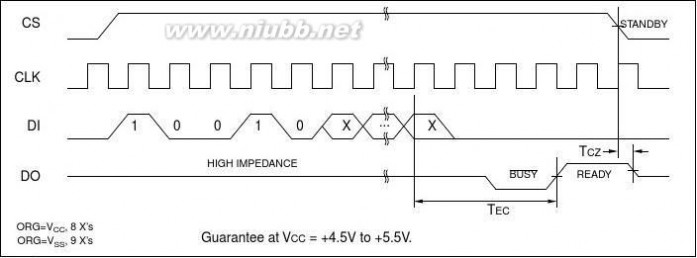
the least signi?cant 8 or 9 address bits are don’t carebits, depending on selection of x16 or x8 mode. Clock-ing of the CLK pin is not necessary after the device hasentered the self clocking mode. The ERAL instruction isguaranteed at Vcc = +4.5V to +5.5V.
be displayed on the DO pin until the next start bit isreceived as long as CS is high. Bringing the CS low willplace the device in standby mode and cause the DO pinto enter the high impedance state. DO at logical “0” indi-cates that programming is still in progress. DO at logical“1” indicates that the entire device has been erased andis ready for another instruction.
The ERAL cycle takes 15 ms maximum (8 ms typical).
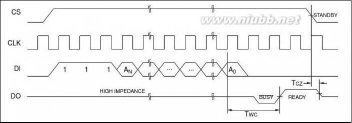
3.2The ERASE instruction forces all data bits of the spec-i?ed address to the logical “1” state. The self-timed pro-gramming cycle is initiated on the rising edge of CLK asthe last address bit (A0) is clocked in. At this point, theCLK, CS, and DI inputs become don’t cares.
be displayed on the DO pin until the next start bit isreceived as long as CS is high. Bringing the CS low willplace the device in standby mode and cause the DO pinto enter the high impedance state. DO at logical “0” indi-cates that programming is still in progress. DO at logical“1” indicates that the register at the speci?ed addresshas been erased and the device is ready for anotherinstruction.
The ERASE cycle takes 3 ms per word (Typical).
3.5The WRAL instruction will write the entire memory arraywith the data speci?ed in the command. The WRALcycle is completely self-timed and commences on therising edge of the last address bit (A0). Note that theleast signi?cant 8 or 9 address bits are don’t cares,depending on selection of x16 or x8 mode. Clocking ofthe CLK pin is not necessary after the device hasentered the self clocking mode. The WRAL commanddoes include an automatic ERAL cycle for the device.Therefore, the WRAL instruction does not require anERAL instruction but the chip must be in the EWEN sta-tus. The WRAL instruction is guaranteed at Vcc = +4.5Vto +5.5V.
be displayed on the DO pin until the next start bit isreceived as long as CS is high. Bringing the CS low willplace the device in standby mode and cause the DO pinto enter the high impedance state. DO at logical “0” indi-cates that programming is still in progress. DO at logical“1” indicates that the entire device has been written andis ready for another instruction.
The WRAL cycle takes 30 ms maximum (16 ms typical).
3.3The WRITE instruction is followed by 16 bits (or by 8bits) of data to be written into the speci?ed address.The self-timed programming cycle is initiated on the ris-ing edge of CLK as the last data bit (D0) is clocked in.At this point, the CLK, CS, and DI inputs become don’tcares.
be displayed on the DO pin until the next start bit isreceived as long as CS is high. Bringing the CS low willplace the device in standby mode and cause the DO pinto enter the high impedance state. DO at logical “0” indi-cates that programming is still in progress. DO at logical“1” indicates that the register at the speci?ed addresshas been written and the device is ready for anotherinstruction.
The WRITE cycle takes 3 ms per word (Typical).
3.4The ERAL instruction will erase the entire memoryarray to the logical “1” state. The ERAL cycle is identicalto the ERASE cycle except for the different opcode. TheERAL cycle is completely self-timed and commenceson the rising edge of the last address bit (A0). Note that
DS21132C-page 6
Preliminary
? 1996 Microchip Technology Inc.
86中文 93C86中文资料
元器件交易网www.cecb2b.com
93C76/86
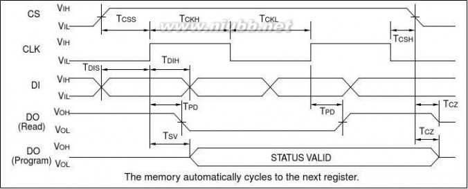
FIGURE 3-2:
CS
READ
TCSL
CLK
DI
110
AN
A0
DO
HIGH IMPEDANCE
DN
D0DN
D0
FIGURE 3-3:EWEN
CS
EWEN
TCSL
CLKDI
...
ORG=VCC, 8 X’sORG=VSS, 9 X’s
1001
1XX
FIGURE 3-4:EWDS
CS
TCSL
CLKDI
...
10000XX
ORG=VCC, 8 X’sORG=VSS, 9 X’S
? 1996 Microchip Technology Inc.
Preliminary
DS21132C-page 7
86中文 93C86中文资料
元器件交易网www.cecb2b.com
93C76/86
DS21132C-page 8Preliminary? 1996 Microchip Technology Inc.

86中文 93C86中文资料
元器件交易网www.cecb2b.com
93C76/86

4.0
4.1
PIN DESCRIPTIONS
Table 1-7 for more details). CLK and DI then becomedon't care inputs waiting for a new start condition to bedetected.A HIGH level selects the device. A LOW level deselectsthe device and forces it into standby mode. However, aprogramming cycle which is already initiated will becompleted, regardless of the CS input signal. If CS isbrought LOW during a program cycle, the device will gointo standby mode as soon as the programming cycleis completed.
CS must be LOW for 250 ns minimum (TCSL) betweenconsecutive instructions. If CS is LOW, the internal con-trol logic is held in a RESET status.
4.3Data In is used to clock in a START bit, opcode,address, and data synchronously with the CLK input.
4.44.2The Serial Clock is used to synchronize the communi-cation between a master device and the 93C76/86.Opcode, address, and data bits are clocked in on thepositive edge of CLK. Data bits are also clocked out onthe positive edge of CLK.
CLK can be stopped anywhere in the transmissionsequence (at HIGH or LOW level) and can be continuedanytime with respect to clock HIGH time (TCKH) andclock LOW time (TCKL). This gives the controlling mas-ter freedom in preparing opcode, address, and data.CLK is a “Don't Care” if CS is LOW (device deselected).If CS is HIGH, but START condition has not beendetected, any number of clock cycles can be receivedby the device without changing its status (i.e., waitingfor START condition).
CLK cycles are not required during the self-timedWRITE (i.e., auto ERASE/WRITE) cycle.
After detection of a start condition the speci?ed numberof clock cycles (respectively LOW to HIGH transitions ofCLK) must be provided. These clock cycles arerequired to clock in all opcode, address, and data bitsbefore an instruction is executed (see Table 1-4 through
Data Out is used in the READ mode to output data syn-chronously with the CLK input (TPD after the positiveedge of CLK).
tus information is available when CS is high. It will bedisplayed until the next start bit occurs as long as CSstays high.
4.5When ORG is connected to VCC, the x16 memory orga-nization is selected. When ORG is tied to VSS, the x8memory organization is selected. There is an internalpull-up resistor on the ORG pin that will select x16 orga-nization when left unconnected.
4.6This pin allows the user to enable or disable the abilityto write data to the memory array. If the PE pin is?oated or tied to VCC, the device can be programmed.If the PE pin is tied to VSS, programming will be inhib-ited. There is an internal pull-up on this device thatenables programming if this pin is left ?oating.
? 1996 Microchip Technology Inc.
Preliminary
DS21132C-page 9
86中文 93C86中文资料
元器件交易网www.cecb2b.com
93C76/86
NOTES:
DS21132C-page 10Preliminary? 1996 Microchip Technology Inc.
86中文 93C86中文资料
元器件交易网www.cecb2b.com
93C76/86
To order or obtain information, e.g., on pricing or delivery, please use the listed part numbers, and refer to the factory or the listedProducts supported by a preliminary Data Sheet may possibly have an errata sheet describing minor operational differences and recommended workarounds. To determine if an errata sheet exists for a particular device, please contact one of the following:
1.Your local Microchip sales of?ce (see below)
2.The Microchip Corporate Literature Center U.S. FAX: (602) 786-7277
3.The Microchip’s Bulletin Board, via your local CompuServe number (CompuServe membership NOT required).
Please specify which device, revision of silicon and Data Sheet (include Literature #) you are using.
For latest version information and upgrade kits for Microchip Development Tools, please call 1-800-755-2345 or 1-602-786-7302.
DS21132C-page 11

Preliminary? 1996 Microchip Technology Inc.
86中文 93C86中文资料
元器件交易网www.cecb2b.com
AMERICAS
Corporate Of?ce
Microchip Technology Inc.2355 West Chandler Blvd.Chandler, AZ 85224-6199
Tel: 602 786-7200 Fax: 602 786-7277Technical Support: 602 786-7627Web: http://www.microchip.comAtlanta
Microchip Technology Inc.
500 Sugar Mill Road, Suite 200BAtlanta, GA 30350
Tel: 770 640-0034 Fax: 770 640-0307Boston
Microchip Technology Inc.5 Mount Royal AvenueMarlborough, MA 01752
Tel: 508 480-9990 Fax: 508 480-8575Chicago
Microchip Technology Inc.333 Pierce Road, Suite 180Itasca, IL 60143
Tel: 708 285-0071 Fax: 708 285-0075Dallas
Microchip Technology Inc.
14651 Dallas Parkway, Suite 816Dallas, TX 75240-8809
Tel: 972 991-7177 Fax: 972 991-8588Dayton
Microchip Technology Inc.Suite 150
Two Prestige PlaceMiamisburg, OH 45342
Tel: 513 291-1654 Fax: 513 291-9175Los Angeles
Microchip Technology Inc.
18201 Von Karman, Suite 1090Irvine, CA 92612
Tel: 714 263-1888 Fax: 714 263-1338New York
Microchip Technology Inc.150 Motor Parkway, Suite 416Hauppauge, NY 11788
Tel: 516 273-5305 Fax: 516 273-5335San Jose
Microchip Technology Inc.
2107 North First Street, Suite 590San Jose, CA 95131
Tel: 408 436-7950 Fax: 408 436-7955Toronto
Microchip Technology Inc.5925 Airport Road, Suite 200
Mississauga, Ontario L4V 1W1, Canada Tel: 905 405-6279Fax: 905 405-6253
ASIA/PACIFIC
Hong Kong
Microchip TechnologyRM 3801B, Tower TwoMetroplaza
223 Hing Fong Road
Kwai Fong, N.T. Hong Kong
Tel: 852 2 401 1200 Fax: 852 2 401 3431India
Microchip Technology
No. 6, Legacy, Convent RoadBangalore 560 025 India
Tel: 91 80 526 3148 Fax: 91 80 559 9840Korea
Microchip Technology
168-1, Youngbo Bldg. 3 FloorSamsung-Dong, Kangnam-Ku,Seoul, Korea
Tel: 82 2 554 7200 Fax: 82 2 558 5934Shanghai
Microchip Technology
Unit 406 of Shanghai Golden Bridge Bldg.2077 Yan’an Road West, Hongiao DistrictShanghai, Peoples Republic of ChinaTel: 86 21 6275 5700
Fax: 011 86 21 6275 5060 Singapore
Microchip Technology200 Middle Road#10-03 Prime CentreSingapore 188980
Tel: 65 334 8870 Fax: 65 334 8850Taiwan, R.O.C
Microchip Technology 10F-1C 207
Tung Hua North RoadTaipei, Taiwan, ROC
Tel: 886 2 717 7175 Fax: 886 2 545 0139
EUROPE
United Kingdom
Arizona Microchip Technology Ltd.Unit 6, The Courtyard
Meadow Bank, Furlong Road
Bourne End, Buckinghamshire SL8 5AJTel: 44 1628 850303 Fax: 44 1628 850178France
Arizona Microchip Technology SARLZone Industrielle de la Bonde2 Rue du Buisson aux Fraises91300 Massy - France
Tel: 33 1 69 53 63 20 Fax: 33 1 69 30 90 79Germany
Arizona Microchip Technology GmbHGustav-Heinemann-Ring 125D-81739 Muenchen, Germany
Tel: 49 89 627 144 0 Fax: 49 89 627 144 44Italy
Arizona Microchip Technology SRL
Centro Direzionale Colleone Pas Taurus 1Viale Colleoni 1
20041 Agrate BrianzaMilan Italy
Tel: 39 39 6899939 Fax: 39 39 689 9883
JAPAN
Microchip Technology Intl. Inc.Benex S-1 6F
3-18-20, Shin YokohamaKohoku-Ku, YokohamaKanagawa 222 Japan
Tel: 81 45 471 6166 Fax: 81 45 471 6122
11/7/96
All rights reserved. ? 1996, Microchip Technology Incorporated, USA. 11/96
Printed on recycled paper.
DS21132C-page 12
? 1996 Microchip Technology Inc.
三 : CA4211-000中文资料
元器件交易网www.cecb2b.com
扩展:74hc000 中文资料 / 7550 1中文资料 / mv3581中文资料
本文标题:中文资料-IAQ中文资料61阅读| 精彩专题| 最新文章| 热门文章| 苏ICP备13036349号-1