一 : MACH5中文资料
MACH 5 CPLD Family
Fifth Generation MACH Architecture
FEATURES
xHigh logic densities and I/Os for increased logic integration
x
x
x
x
x
x
x—128 to 512 macrocell densities—68 to 256 I/OsWide selection of density and I/O combinations to support most application needs—6 macrocell density options—7 I/O options —Up to 4 I/O options per macrocell density—Up to 5 density & I/O options for each packagePerformance features to ?t system needs—5.5 ns tPD Commercial, 7.5 ns tPD Industrial—182 MHz fCNT—Four programmable power/speed settings per block Flexible architecture facilitates logic design—Multiple levels of switch matrices allow for performance-based routing—100% routability and pin-out retention—Synchronous and asynchronous clocking, including dual-edge clocking—Asynchronous product- or sum-term set or reset—16 to 64 output enables—Functions of up to 32 product termsAdvanced capabilities for easy system integration—3.3-V & 5-V JEDEC-compliant operations—IEEE 1149.1 compliant for boundary scan testing—3.3-V & 5-V in-system programmable via IEEE 1149.1 Boundary Scan Test Access Port—PCI compliant (-5/-6/-7/-10/-12 speed grades)—Safe for mixed supply voltage system design—Bus-Friendly? Inputs & I/Os—Individual output slew rate control—Hot socketing—Programmable security bitAdvanced E2CMOS process provides high performance, cost effective solutionsSupported by ispDesignEXPERT? software for rapid logic development—Supports HDL design methodologies with results optimized for MACH 5 devices—Flexibility to adapt to user requirements—Software partnerships that ensure customer successLattice and Third-party hardware programming support
—LatticePRO? software for in-system programmability support on PCs and Automated Test Equipment
—Programming support on all major programmers including Data I/O, BP Microsystems, Advin, and System General
Publication# 20446
Amendment/0Rev: IIssue Date: September 2000
mach5 MACH5中文资料
Table 1. MACH 5 Device Features 1
Feature
Supply Voltage (V)Macrocells
Maximum User I/O Pins(ns)tPD tSS (ns)tCOS (ns)fCNT (MHz)
Typical Static Power (mA)
IEEE 1149.1 Boundary Scan CompliantPCI-Compliant
M5-128/1
M5LV-12851281203.04.518235YesYes
3.31281203.04.518235YesYes
M5-192/1
51921203.04.518245YesYes
M5-256/1M5LV-25652561603.04.518255YesYes
3.32561603.04.518255YesYes
M5-320M5LV-32053201923.025.0167270YesYes
3.33201926.53.025.0167270YesYes
M5-384M5LV-38453841606.53.025.0167275YesYes
3.33841926.53.025.0167275YesYes
M5-512M5LV-51255122566.53.025.01672100YesYes
3.35122566.53.025.01672100YesYes
6.5Note:
1.“M5-xxx” is for 5-V devices. “M5LV-xxx” is for 3.3-V devices.
2.Preliminary speci?cations for new 6.5ns (Tpd) speed grade. 7.5ns speed grade in production now.
GENERAL DESCRIPTION
The MACH? 5 family consists of a broad range of high-density and high-I/O Complex
Programmable Logic Devices (CPLDs). The ?fth-generation MACH architecture yields fast speeds at high CPLD densities, low power, and supports additional features such as in-system
programmability, Boundary Scan testability, and advanced clocking options (Table 1). The MACH 5 family offers 5-V (M5-xxx) and 3.3-V (M5LV-xxx) operation.
Manufactured in state-of-the-art ISO 9000 quali?ed fabrication facilities on E2CMOS process
technologies, MACH 5 devices are available with pin-to-pin delays as fast as 5.5 ns (Table 2). The 5.5, 6.5, 7.5, 10, and 12-ns devices are compliant with the PCI Local Bus Speci?cation.
2MACH 5 Family
mach5 MACH5中文资料
Table 2. MACH 5 Speed Grades
Speed GradeDevice
M5-128M5-128/1M5LV-128M5-192/1M5-2562M5-256/1M5LV-256M5-320M5LV-320M5-384M5LV-384M5-512M5LV-512
CC
CCCC3CC3
CCC-5
-6
-7CC, IC,IC, ICC, IC, IC, IC, IC, IC, I3C, IC, I3
-10C, IC, IC, IC, IC, IC, IC, IC, IC, IC, IC, IC, IC, I
-12C, IC, IC, IC, IC, IC, IC, IC, IC, IC, IC, IC, IC, I
-15C, IC, IIC, IC, IC, IIC, IC, IC, IC, IC, IC, I
IIIIIIIII-20II
Note:
1.C = Commercial grade, I = Industrial grade 2./1 version recommended for new designs3.Preliminary speci?catons
With Lattice’s unique hierarchical architecture, the MACH 5 family provides densities up to 512 macrocells to support full system logic integration. Extensive routing resources ensure pinout retention as well as high utilization. It is ideal for PAL? block device integration and a wide range of other applications including high-speed computing, low-power applications, communications, and embedded control. At each macrocell density point, Lattice offers several I/O and package options to meet a wide range of design needs (Table 3).
Table 3. MACH 5 Package and I/O Options 1
扩展:mach4中文版 / mach3中文版下载 / mach3.043中文破解版
M5-128/1M5LV-128
Supply Voltage100-pin TQFP100-pin PQFP144-pin TQFP144-pin PQFP160-pin PQFP208-pin PQFP240-pin PQFP256-ball BGA352-ball BGA
Note:
1.The I/O options indicated with a “*” are obsolete, please contact factory for more information.
10412056868
3.368, 7468*104104*120
104*120
104*120160
M5-192/1
56868*
M5-256/1M5LV-25656868*
3.368*, 7468104104*120160
120*160184*192
120160184*192*
120*160184*192*
120160184*192*
120*160184*192*256
120160184*192*256
M5-320M5LV-3205
3.3
M5-384M5LV-3845
3.3
M5-512M5LV-5125
3.3
MACH 5 Family3
mach5 MACH5中文资料
Advanced power management options allow designers to incrementally reduce power while maintaining the level of performance needed for today’s complex designs. I/O safety features allow for mixed-voltage design, and both the 3.3-V and the 5-V device versions are in-system programmable through an IEEE 1149.1 Test Access Port (TAP) interface.
FUNCTIONAL DESCRIPTION
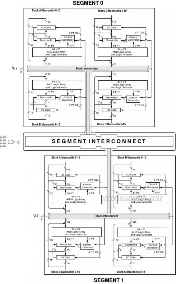
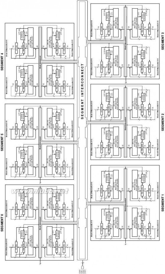
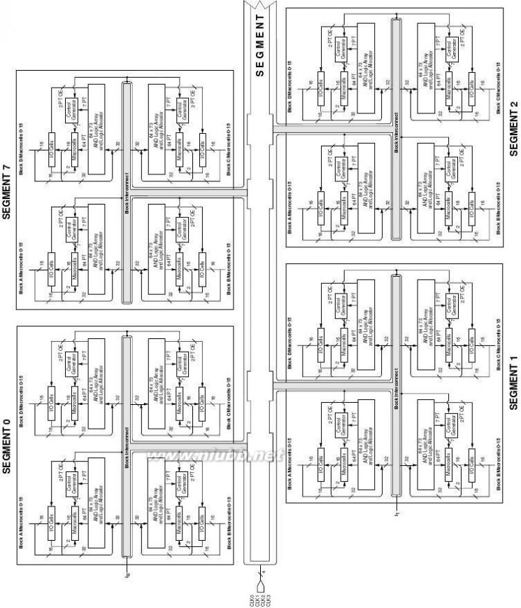
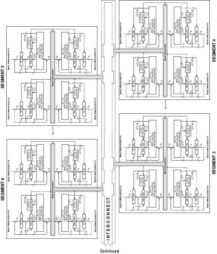
The MACH 5 architecture consists of PAL blocks connected by two levels of interconnect. The block interconnect provides routing among 4 PAL blocks. This grouping of PAL blocks joined by the block interconnect is called a segment. The second level of interconnect, the segment interconnect, ties all of the segments together. The only logic difference between any two MACH 5 devices is the number of segments. Therefore, once a designer is familiar with one device,
consistent performance can be expected across the entire family. All devices have four clock pins available which can also be used as logic inputs.
20446G-001
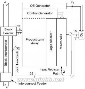
Figure 1. MACH 5 Block Diagram
The MACH 5 PAL blocks consist of the elements listed below (Figure 2). While each PAL block resembles an independent PAL device, it has superior control and logic generation capabilities.x
x
x
x
xI/O cellsProduct-term array and Logic AllocatorMacrocellsRegister control generatorOutput enable generator
I/O Cells
The I/Os associated with each PAL block have a path directly back to that PAL block called local feedback. If the I/O is used in another PAL block, the interconnect feeder assigns a block interconnect line to that signal. The interconnect feeder acts as an input switch matrix. The block and segment interconnects provide connections between any two signals in a device. The block feeder assigns block interconnect lines and local feedback lines to the PAL block inputs.

4MACH 5 Family
mach5 MACH5中文资料
20446G-002
Figure 2. PAL Block Structure
Product-Term Array and Logic Allocator
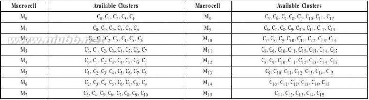
The product-term array uses the same sum-of-products architecture as PAL devices and consists of 32 inputs (plus their complements) and 64 product terms arranged in 16 clusters. A cluster is a sum-of-products function with either 3 of 4 product terms.
Logic allocators assign the clusters to macrocells. Each macrocell can accept up to eight clusters of three or four product terms, but a given cluster can only be steered to one macrocell (Table 4). If only three product terms in a cluster are steered, the fourth can be used as an input to an XOR gate for separate logic generation and/or polarity control.
The wide logic allocator is comprised of all 16 of the individual logic allocators and acts as an output switch matrix by reassigning logic to macrocells to retain pinout as designs change. The logic allocation scheme in the MACH 5 device allows for the implementation of large equations (up to 32 product terms) with only one pass through the logic array.
Table 4. Product Term Steering Options for PT Clusters and Macrocells
MACH 5 Family
5
mach5 MACH5中文资料
Macrocells
The macrocells for MACH 5 devices consist of a storage element which can be con?gured for combinatorial, registered or latched operation (Figure 3). The D-type ?ip-?ops can be con?gured as T-type, J-K, or S-R operation through the use of the XOR gate associated with each macrocell.Each PAL block has the capability to provide two input registers by using macrocells 0 and 15. In order to use this option, these macrocells must be accessed via the I/O pins associated with macrocells 3 and 12, respectively. Once the macrocell is used as an input register, it cannot be used for logic, so its clusters can be re-directed through the logic allocator to another macrocell. The I/O pins associated with macrocells 0 and 15 can still be used as input pins. Although the I/O pins for macrocells 3 and 12 are used to connect to the input registers, these macrocells can still be used as “buried” macrocells to drive device logic via the matrix.
扩展:mach4中文版 / mach3中文版下载 / mach3.043中文破解版
20446G-003
Figure 3. Macrocell Diagram
Control Generator
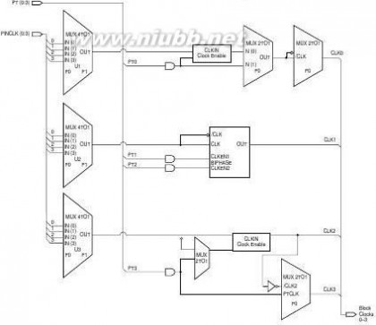
The control generator provides four con?gurable clock lines and three con?gurable set/reset lines to each macrocell in a PAL block. Any of the four clock lines and any of the three set/reset lines can be independently selected by any ?ip-?op within a block. The clock lines can be con?gured to provide synchronous global (pin) clocks and asynchronous product term clocks, sum term clocks, and latch enables (Figure 4). Three of the four global clocks, as well as two product-term clocks and one sum-term clock, are available per PAL block. Positive or negative edge clocking is available as well as advanced clocking features such as complementary and biphase clocking. Complementary clocking provides two clock lines exactly 180 degrees out of phase, and is useful in applications such as fast data paths. A biphase clock line clocks ?ip-?ops on both the positive and negative edges of the clock. The con?guration options for the four clock lines per PAL block are as follows:
Clock Line 0 Options
x
x
xGlobal clock (0, 1, 2, or 3) with positive or negative edge clock enableProduct-term clock (A*B*C)Sum-term clock (A+B+C)

6MACH 5 Family
mach5 MACH5中文资料
Clock Line 1 Optionsxxx
Global clock (0, 1, 2, or 3) with positive edge clock enableGlobal clock (0, 1, 2, or 3) with negative edge clock enable
Global clock (0, 1, 2, or 3) with positive and negative edge clock enable (biphase)Global clock (0, 1, 2, or 3) with clock enableComplement of clock line 2 (same clock enable)
Product-term clock (if clock line 2 does not use clock enable
Clock Line 2 Optionsx
Clock Line 3 Optionsxx
20446G-004
20446G-005
Figure 4. Clock Generator
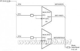
Figure 5. Set/Reset Generator
The set/reset generation portion of the control generator (Figure 5) creates three set/reset lines for the PAL block. Each macrocell can choose one of these three lines or choose no set/reset at all. All three lines can be con?gured for product term set/reset and two of the three lines can be con?gured as sum term set/reset and one of the lines can be con?gured as product-term or sum-term latch enable. While the set/reset signals are generated in the control generator, whether that signal sets or resets a ?ip-?op is determined within the individual macrocell. The same signal can set one ?ip-?op and reset another. PT2 or /PT2 can also be used as a latch enable for macrocells con?gured as latches.
MACH 5 Family7
mach5 MACH5中文资料
OE Generator
There is one output enable (OE) generator per PAL block that generates two product-term driven output enables. Each I/O cell is simply an output buffer. Each I/O cell within the PAL block can choose to be permanently enabled, permanently disabled, or choose one of the two product term output enables per PAL block (Figure 6).
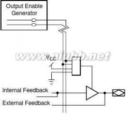
20446G-006
Figure 6. Output Enable Generator and I/O Cell
8MACH 5 Family
mach5 MACH5中文资料
MACH 5 TIMING MODEL
The primary focus of the MACH 5 timing model is to accurately represent the timing in a MACH 5 device, and at the same time, be easy to understand. This model accurately describes all
combinatorial and registered paths through the device, making a distinction between internal
feedback and external feedback. A signal uses internal feedback when it is fed back into the switch matrix or block without having to go through the output buffer. The input register speci?cations are also reported as internal feedback. When a signal is fed back into the switch matrix after having gone through the output buffer, it is using external feedback.
The parameter, tBUF, is de?ned as the time it takes to go through the output buffer to the I/O pad. If a signal goes to the internal feedback rather than to the I/O pad, the parameter designator is followed by an “i”. By adding tBUF to this internal parameter, the external parameter is derived. For example, tPD = tPDi + tBUF. A diagram representing the modularized MACH 5 timing model is shown in Figure 7. Refer to the Technical Note entitled MACH 5 Timing and High Speed Design for a more detailed discussion about the timing parameters.
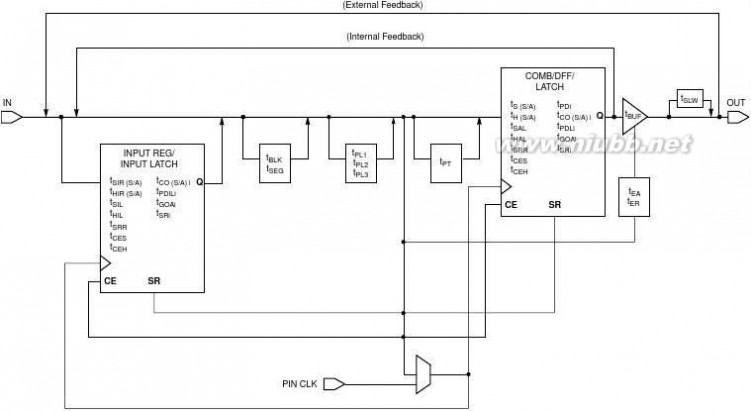
20446G-014
Figure 7. MACH 5 Timing Model
MACH 5 Family9
mach5 MACH5中文资料
MULTIPLE I/O AND DENSITY OPTIONS
扩展:mach4中文版 / mach3中文版下载 / mach3.043中文破解版
The MACH 5 family offers six macrocell densities in a number of I/O options. This allows designers to choose a device close to their logic density and I/O requirements, thus minimizing costs. For the same package type, every density has the same pin-out. With proper design considerations, a design can be moved to a higher or lower density part as required.
IEEE 1149.1 - COMPLIANT BOUNDARY SCAN TESTABILITY
Most MACH 5 devices have boundary scan registers and are compliant to the IEEE 1149.1 standard. This allows functional testing of the circuit board on which the device is mounted through a serial scan path that can access all critical logic nodes. Internal registers are linked internally, allowing test data to be shifted in and loaded directly onto test nodes, or test node data to be captured and shifted out for veri?cation. In addition, these devices can be linked into a board-level serial scan path for more complete board-level testing.
IEEE 1149.1 - COMPLIANT IN-SYSTEM PROGRAMMING
Programming devices in-system provides a number of signi?cant bene?ts including: rapid
prototyping, lower inventory levels, higher quality, and the ability to make in-?eld modi?cations. All MACH 5 devices provide in-system programming (ISP) capability through their IEEE 1149.1-compliant Boundary Scan Test Access Port. By using the IEEE 1149.1-compliant Boundary Scan Test Access Port as the communication interface through which ISP is achieved, customers get the bene?t of a standard, well-de?ned interface.
MACH 5 devices can be programmed across the commercial temperature and voltage range. The PC-based LatticePRO software facilitates in-system programming of MACH 5 devices. LatticePRO software takes the JEDEC ?le output produced by design implementation software, along with information about the Boundary Scan chain, and creates a set of vectors that are used to drive the Boundary Scan chain. LatticePRO software can use these vectors to drive a Boundary Scan chain via the parallel port of a PC. Alternatively, LatticePRO software can output ?les in formats
understood by common automated test equipment. This equipment can then be used to program MACH 5 devices during the testing of a circuit board.
PCI COMPLIANT
MACH 5 devices in the -5/-6/-7/-10/-12 speed grades are compliant with the PCI Local Bus
Speci?cation version 2.1, published by the PCI Special Interest Group (SIG). The 5-V devices are fully PCI-compliant. The 3.3-V devices are mostly compliant but do not meet the PCI condition to clamp the inputs as they rise above VCC because of their 5-V input tolerant feature. MACH 5 devices provide the speed, drive, density, output enables and I/Os for the most complex PCI designs.
10MACH 5 Family
mach5 MACH5中文资料
SAFE FOR MIXED SUPPLY VOLTAGE SYSTEM DESIGNS 1
Both the 3.3-V and 5-V VCC MACH 5 devices are safe for mixed supply voltage system designs. The 5-V devices will not overdrive 3.3-V devices above the output voltage of 3.3 V, while they accept inputs from other 3.3-V devices. The 3.3-V devices will accept inputs up to 5.5 V. Both the
3.3-V and 5-V versions have the same high-speed performance and provide easy-to-use mixed-voltage design capability.
Note:
1.Excludes original M5-128, M5-192, and M5-256 while M5-128/1, M3-192/1 and M5-256/1 are supported. Please refer to Application Note titled “Hot Socketing and Mixed Supply Design with MACH 4 and MACH 5 Devices”.
BUS-FRIENDLY INPUTS AND I/OS
All MACH 5 devices have inputs and I/Os which feature the Bus-Friendly circuitry incorporating two inverters in series which loop back to the input. This double inversion weakly holds the input at its last driven logic state. While it is a good design practice to tie unused pins to a known state, the Bus-Friendly input structure pulls pins away from the input threshold voltage where noise can cause high-frequency switching. At power-up, the Bus-Friendly latches are reset to a logic level “1.” For the circuit diagram, please refer to the document entitled MACH Endurance Characteristics on the Lattice Data Book CD-ROM or Lattice web site.
POWER MANAGEMENT
There are 4 power/speed options in each MACH 5 PAL block (Table 5). The speed and power tradeoff can be tailored for each design. The signal speed paths in the lower-power PAL blocks will be slower than those in the higher-power PAL blocks. This feature allows speed critical paths to run at maximum frequency while the rest of the signal paths operate in a lower-power mode. In large designs, there may be several different speed requirements for different portions of the design.
Table 5. Power LevelsHigh Speed/High Power
Medium High Speed/Medium High Power
Medium Low Speed/Medium Low Power
Low Speed/Low Power100% Power67% Power40% Power20% Power
PROGRAMMABLE SLEW RATE
Each MACH 5 device I/O has an individually programmable output slew rate control bit. Each output can be individually con?gured for the higher speed transition (3 V/ns) or for the lower noise transition (1 V/ns). For high-speed designs with long, unterminated traces, the slow-slew rate will introduce fewer re?ections, less noise, and keep ground bounce to a minimum. For designs with short traces or well terminated lines, the fast slew rate can be used to achieve the highest speed. The slew rate is adjusted independent of power.
扩展:mach4中文版 / mach3中文版下载 / mach3.043中文破解版
POWER-UP RESET/SET
All ?ip-?ops power up to a known state for predictable system initialization. If a macrocell is con?gured to SET on a signal from the control generator, then that macrocell will be SET during device power-up. If a macrocell is con?gured to RESET on a signal from the control generator or is not con?gured for set/reset, then that macrocell will RESET on power-up. To guarantee
MACH 5 Family11
mach5 MACH5中文资料
initialization values, the VCC rise must be monotonic and the clock must be inactive until the reset delay time has elapsed.
SECURITY BIT
A programmable security bit is provided on the MACH 5 devices as a deterrent to unauthorized copying of the array con?guration patterns. Once programmed, this bit defeats readback of the programmed pattern by a device programmer, securing proprietary designs from competitors. Programming and veri?cation are also defeated by the security bit. The bit can only be reset by erasing the entire device.
12MACH 5 Family
mach5 MACH5中文资料
MACH 5 PAL BLOCK

MACH 5 Family13
mach5 MACH5中文资料
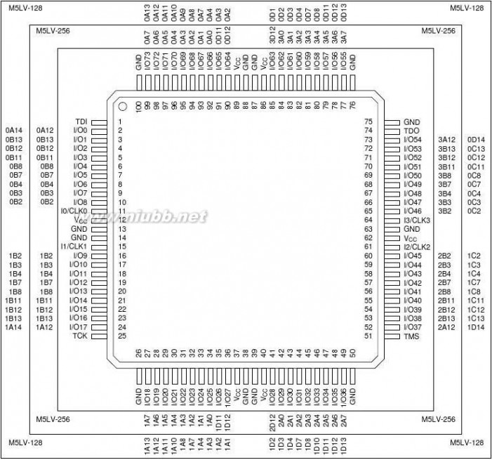
BLOCK DIAGRAM — M5(LV)-128/XXX
20446G-007
14MACH 5 Family
mach5 MACH5中文资料
BLOCK DIAGRAM — M5-192/XXX

MACH 5 Family
15
mach5 MACH5中文资料
16
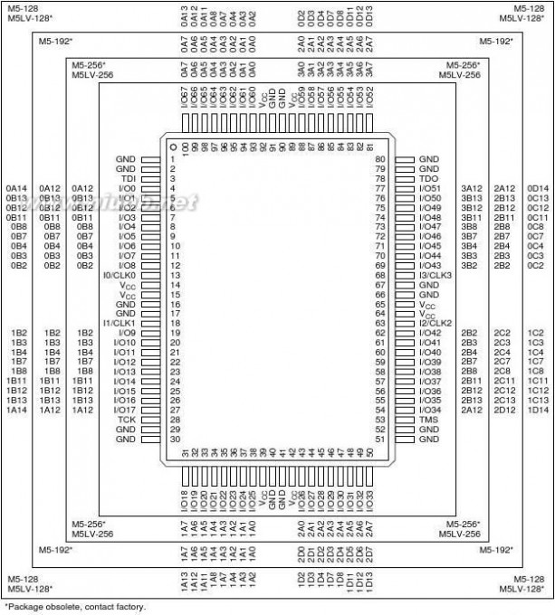
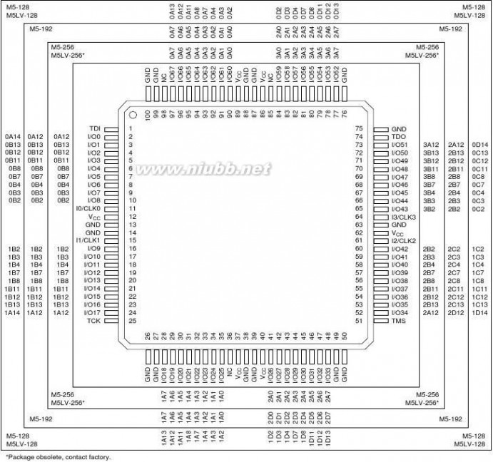
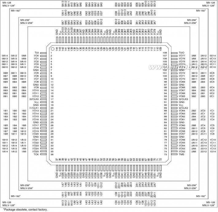
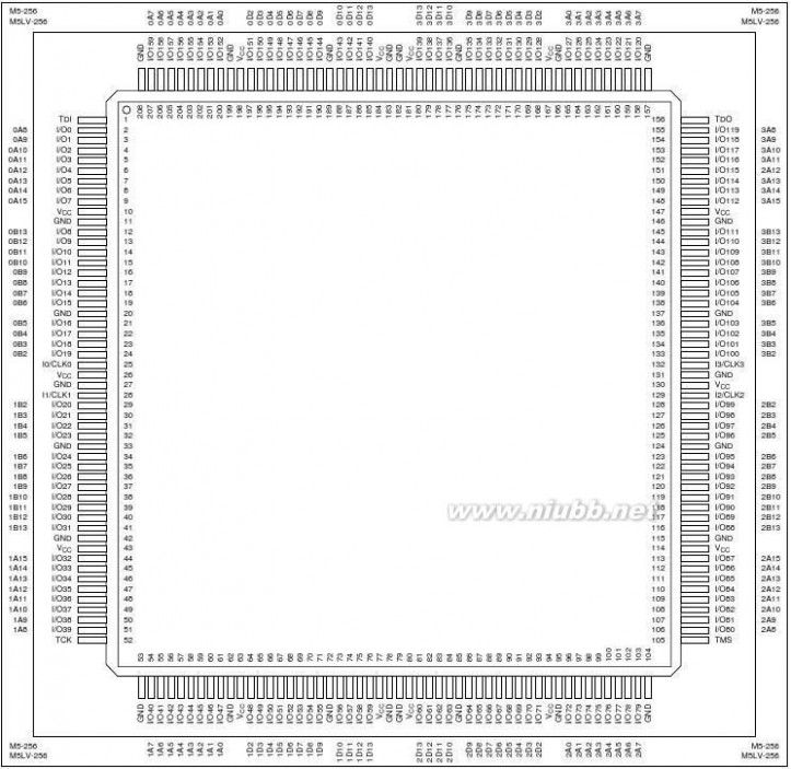
BLOCK DIAGRAM — M5(LV)-256/XXX

MACH 5 Family
mach5 MACH5中文资料
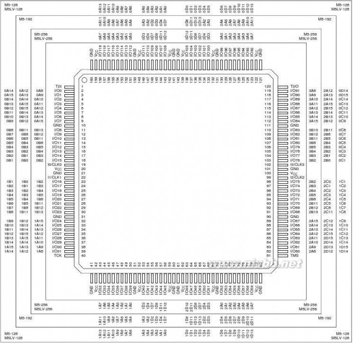
BLOCK DIAGRAM — M5(LV)-320/XXX
MACH 5 Family
17
mach5 MACH5中文资料
18
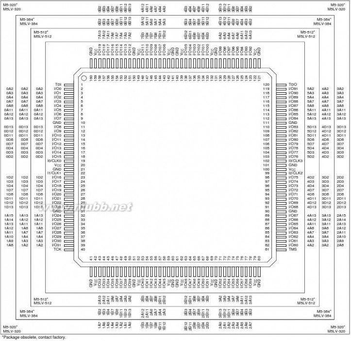
BLOCK DIAGRAM — M5(LV)-384/XXX
MACH 5 Family
20446G-011
mach5 MACH5中文资料
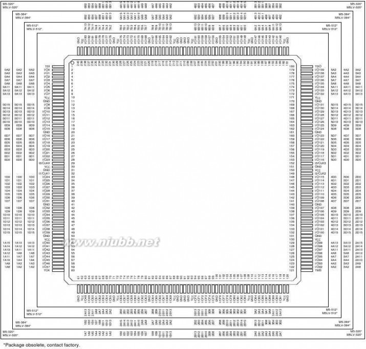
BLOCK DIAGRAM — M5(LV)-512/XXX
Continued
MACH 5 Family
20446G-012
19
mach5 MACH5中文资料
20
BLOCK DIAGRAM — M5(LV)-512/XXX
MACH 5 Family
20446G-013
mach5 MACH5中文资料
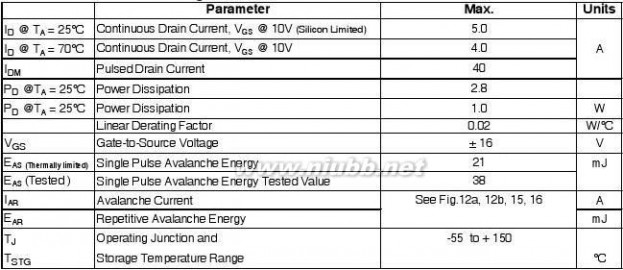
ABSOLUTE MAXIMUM RATINGS
M5
Storage Temperature. . . . . . . . . . . . . .-65°C to +150°CDevice Junction
Temperature (Note 1) . . . . . . . . . . . +130°C or +150°CSupply Voltage
with Respect to Ground . . . . . . . . . . .-0.5 V to +7.0 VDC Input Voltage . . . . . . . . . . . . . . . . .-0.5 V to 5.5 VStatic Discharge Voltage . . . . . . . . . . . . . . . . . 2000 VLatchup Current (-40°C to +85°C) . . . . . . . . . .200 mA
Stresses above those listed under Absolute MaximumRatings may cause permanent device failure. Functionality ator above these limits is not implied. Exposure to AbsoluteMaximum Ratings for extended periods may affect devicereliability.
OPERATING RANGES
Commercial (C) Devices
Ambient Temperature (TA)
Operating in Free Air. . . . . . . . . . . . . . . 0°C to +70°CSupply Voltage (VCC)
with Respect to Ground. . . . . . . . . +4.75 V to +5.25 V
Industrial (I) Devices
Ambient Temperature (TA)
Operating in Free Air. . . . . . . . . . . . . . -40°C to +85°CSupply Voltage (VCC)
with Respect to Ground. . . . . . . . . . .+4.5 V to +5.5 V
Operating ranges de?ne those limits between which the functionality of the device is guaranteed.
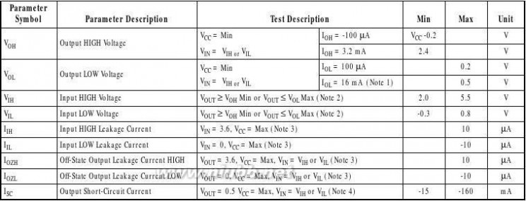
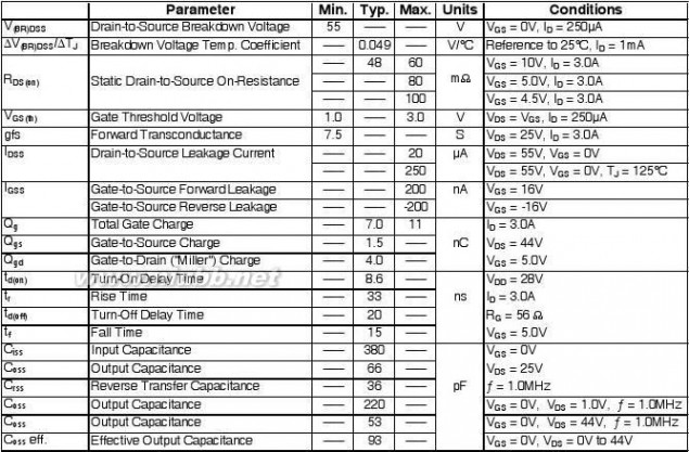
5-V DC CHARACTERISITICS OVER OPERATING RANGES
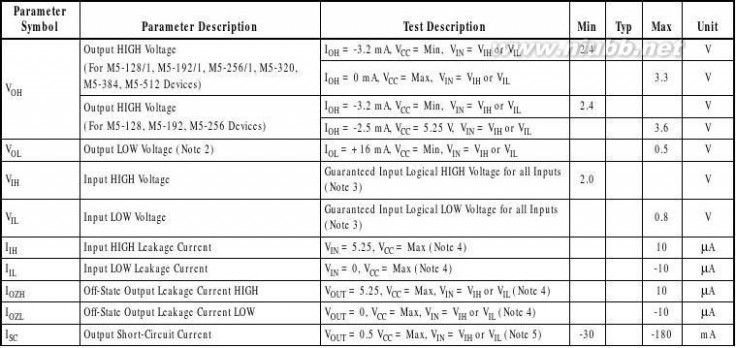
Note:
1.150° for M5-128, M5-192 and M5-256 devices. 130° for M5-128/1, M5-192/1, M5-256/1, M5-320, M5-384 and M5-512 devices.2.Total IOL between ground pins should not exceed 64 mA.
3.These are absolute values with respect to device ground, and all overshoots due to system and/or tester noise are included.4.I/O pin leakage is the worst case of IIL and IOZL or IIH and IOZH.
5.Not more than one output should be shorted at a time. Duration of the short-circuit should not exceed one second.
MACH 5 Family21
mach5 MACH5中文资料
ABSOLUTE MAXIMUM RATINGS
M5LV
Storage Temperature. . . . . . . . . . . . . .-65°C to +150°CDevice Junction Temperature . . . . . . . . . . . . . +130°CSupply Voltage
扩展:mach4中文版 / mach3中文版下载 / mach3.043中文破解版
with Respect to Ground . . . . . . . . . . .-0.5 V to +4.5 VDC Input Voltage . . . . . . . . . . . . . . . . .-0.5 V to 5.5 VStatic Discharge Voltage . . . . . . . . . . . . . . . . . 2000 VLatchup Current (-40°C to +85°C) . . . . . . . . . .200 mA
Stresses above those listed under Absolute MaximumRatings may cause permanent device failure. Functionality ator above these limits is not implied. Exposure to AbsoluteMaximum Ratings for extended periods may affect devicereliability.
OPERATING RANGES
Commercial (C) Devices
Ambient Temperature (TA)
Operating in Free Air. . . . . . . . . . . . . . . 0°C to +70°CSupply Voltage (VCC)
with Respect to Ground. . . . . . . . . . .+3.0 V to +3.6 V
Industrial (I) Devices
Ambient Temperature (TA)
Operating in Free Air. . . . . . . . . . . . . . -40°C to +85°CSupply Voltage (VCC)
with Respect to Ground. . . . . . . . . . .+3.0 V to +3.6 V
Operating ranges de?ne those limits between which the functionality of the device is guaranteed.
3.3-V DC CHARACTERISITICS OVER OPERATING RANGES
Notes:
1.Total IOL between ground pins should not exceed 64 mA.
2.These are absolute values with respect to device ground, and all overshoots due to system and/or tester noise are included.3.I/O pin leakage is the worst case of IIL and IOZL or IIH and IOZH.
4.Not more than one output should be shorted at one time. Duration of the short-circuit should not exceed one second.
22MACH 5 Family
mach5 MACH5中文资料
M5(LV) TIMING PARAMETERS OVER OPERATING RANGES1
-5Min
Combinatorial Delay:tPDitPDtSStSAtHStHAtCOSitCOStCOAitCOAtSALtHALtPDLitPDLtGOAitGOA
Internal combinatorial propagation delay
Combinatorial propagation delaySynchronous clock setup timeAsynchronous clock setup timeSynchronous clock hold timeAsynchronous clock hold timeSynchronous clock to internal outputSynchronous clock to outputAsynchronous clock to internal outputAsynchronous clock to outputLatch setup timeLatch hold timeTransparent latch internal
Propagation delay through transparent latch
Gate to internal outputGate to output
Input register setup time using a synchronous clock
Input register setup time using an asynchronous clock
Input register hold time using a synchronous clock
Input register hold time using an asynchronous clockInput latch setup time Input latch hold time Transparent input latchOutput buffer delaySlow slew rate delayOutput enable timeOutput disable time
3.03.0
6.08.07.09.03.03.00.03.0
2.54.56.08.0
4.03.0
7.09.08.010.0
3.55.5
3.03.00.03.0
3.05.06.08.0
4.04.0
7.09.08.010.0
4.56.5
4.04.00.04.0
4.06.08.010.0
5.05.0
8.010.09.011.0
5.57.5
5.05.00.05.0
5.07.010.012.0
6.06.0
9.011.010.012.0
8.010.0
6.06.00.06.0
6.08.013.015.0
7.07.0
10.012.011.013.0
10.012.0
8.07.00.07.0
8.010.015.017.0
8.08.0
10.012.012.014.0
13.015.0
10.08.00.08.0
10.012.018.020.018.020.0
nsnsnsnsnsnsnsnsnsnsnsnsnsnsnsns
Max
Min
-6Max
Min
-7Max
-10Min
Max
-12Min
Max
-15Min
Max
-20Min
Max
Unit
Registered Delays:
Latched Delays:
Input Register Delays:tSIRStSIRAtHIRStHIRA
2.00.03.06.0
2.00.03.06.0
2.00.03.06.0
3.00.04.07.0
3.00.04.07.0
3.00.04.07.0
3.00.04.07.0
nsnsnsns
Input Latch Delays:tSILtHILtPDILitBUFtSLWtEAtER
2.06.0
5.02.02.57.57.5
2.06.0
5.02.02.57.57.5
2.06.0
5.52.02.59.59.5
3.07.0
6.02.02.510.010.0
3.07.0
6.02.02.512.012.0
3.07.0
6.02.02.515.015.0
3.07.0
6.02.02.520.020.0
nsnsnsnsnsnsns
Output Delays:
MACH 5 Family23
mach5 MACH5中文资料
M5(LV) TIMING PARAMETERS OVER OPERATING RANGES1 (CONTINUED)
-5Min
Power Delays:tPL1tPL2tPL3
Power level 1 delay (Note 2)Power level 2 delay (Note 2)Power level 3 delay (Note 2)
4.0 (5.0)6.0 (9.0)9.0
(17.5)
-6
Max
Min
Max
Min
-7Max4.0 (5.0)6.0 (9.0)9.0
(17.5)
-10Min
Max4.0 (5.0)6.0 (9.0)9.0
(17.5)
-12Min
Max4.0 (5.0)6.0 (9.0)9.0
(17.5)
-15Min
Max4.0 (5.0)6.0 (9.0)9.0
(17.5)
-20Min
Max4.0 (5.0)6.0 (9.0)9.0
(17.5)
Unit
4.06.09.0
nsnsns
Additional Cluster Delay:tPTtBLKtSEG
Product term cluster delayBlock interconnect delaySegment interconnect delay
Asynchronous reset or preset to internal register output
Asynchronous reset or preset to register output
Reset and set register recovery timeAsynchronous reset or preset widthClock enable setup timeClock enable hold timeGlobal clock width low (Note 3)Global clock widthhigh (Note 3)Product term clock width lowProduct term clock width highGate width low (for low transparent) or high (for high transparent)Input register clock width low or high
扩展:mach4中文版 / mach3中文版下载 / mach3.043中文破解版
5.53.04.03.02.52.53.03.03.03.0
0.31.54.5
0.31.54.5
0.31.55.0
0.32.06.0
0.32.06.0
0.32.06.0
0.32.06.0
nsnsns
Interconnect Delays:
Reset and Preset Delays:tSRitSRtSRRtSRWtCEStCEHWidth:tWLStWHStWLAtWHAtGWAtWIR
3.03.04.04.04.04.0
3.03.04.04.04.04.0
4.04.05.05.05.05.0
5.05.06.06.06.06.0
6.06.07.07.07.07.0
6.06.08.08.08.08.0
nsnsnsnsnsns
6.08.0
7.54.05.04.0
8.010.0
7.54.05.04.0
8.010.0
8.05.06.05.0
10.012.0
9.06.07.06.0
12.014.0
10.07.07.06.0
14.016.0
11.08.08.07.0
16.018.0
nsnsnsnsnsns
Clock Enable Delays:
24MACH 5 Family
mach5 MACH5中文资料
M5(LV) TIMING PARAMETERS OVER OPERATING RANGES1 (CONTINUED)
-5Min
Frequency:
External feedback, PAL block level. Min
133
of 1/(tWLS + tWHS) or 1/(tSS + tCOS)fMAX
Internal feedback, PAL block level. Min of 1/(tWLS + tWHS) or 1/(tSS +tCOSi)No feedback PAL block level. Min of 1/(tWLS + tWHS) or 1/(tSS + tHS)External feedback, PAL block level. Min of 1/(tWLA + tWHA) or 1/(tSA + tCOA)fMAXA
18220091
12516716791111125125
10012516771.483.3125125
83.310012558.866.7100100
71.483.310047.652.683.383.3
55.662.583.341.745.571.471.4
45.550.083.335.738.562.562.5
MHzMHzMHzMHzMHzMHzMHz
Max
Min
-6Max
Min
-7Max
-10Min
Max
-12Min
Max
-15Min
Max
-20Min
Max
Unit
Internal feedback, PAL block level. Min
111
of 1/(tWLA + tWHA) or 1/(tSA +tCOAi)No feedback, PAL block level. Min of 1/(tWLA + tWHA) or 1/(tSA + tHA)
167167
fMAXI
Maximum input register frequency 1/(tSIRS+tHIRS) or 1/(2 x tWICW)
Notes:
1.See “MACH Switching Test Circuits” documentation on the Lattice Data Book CD-ROM or Lattice web site.2.Numbers in parentheses are for M5-128, M5-192, M5-256.
3.If a signal is used as both a clock and a logic array input, then the maximum input frequency applies (fMAX/2).
MACH 5 Family25
mach5 MACH5中文资料
CAPACITANCE1
Parameter SymbolCINCI/O
Parameter DescriptionI/CLK pinI/O pin
Test conditions
VIN =2.0 VVOUT =2.0 V
3.3 V or 5 V, 25o C, 1 MHz3.3 V or 5 V, 25o C, 1 MHz
Typ1210
UnitpFpF
1.These parameters are not 100% tested, but are calculated at initial characterization and at any time the design is modi?ed where
these parameters may be affected.
ICC vs. FREQUENCY
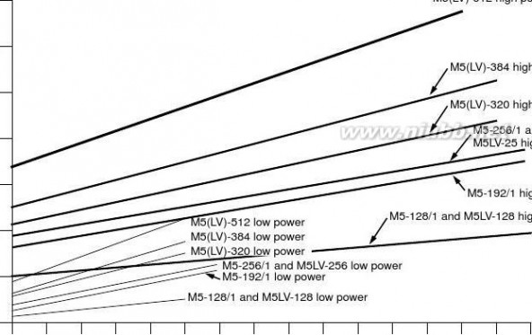
These curves represent the typical power consumption for a particular device at system frequency. The selected “typical” pattern is a 16-bit up-down counter. This pattern ?lls the device and exercises every macrocell. Maximum frequency shown uses internal feedback and a D-type register. Power/Speed are optimized to obtain the highest counter frequency and the lowest power. The highest frequency (LSBs) is placed in common PAL blocks, which are set to high power. The lowest frequency signals (MSBs) are placed in a common PAL block and set to lowest power. For a more detailed discussion about MACH 5 power consumption, refer to the application note entitled MACH 5 Power in the Application Notes section on the Lattice Data Book CD-ROM or Lattice web site.
ICC CURVES AT HIGH /LOW POWER MODES
VCC = 5 V or 3.3 V, TA = 25o C
700
600
500
ICC (mA)
400
300
200
100
100
110
120
130
140
150
20446G-048
10
20
30
40
50
60
70
80
Frequency (MHz)
Figure 8. ICC Curves at High/Low Power Modes
26MACH 5 Family
90
mach5 MACH5中文资料
VCC = 5 V, TA = 25o C
700
M5-256 high power
600
500M5-192 high power
ICC (mA)
400
M5-128 high power
300
200
M5-256 low power
100
M5-192 low powerM5-128 low power
100
110
120
130
140
150
10
20
30
40
50
60
70
80
90
Frequency (MHz)
20446G-049
Figure 9. ICC Curves at High/Low Power Modes
MACH 5 Family27
mach5 MACH5中文资料
100-PIN PQFP CONNECTION DIAGRAM
Top View
100-Pin PQFP (68 I/O)
Pin Designations
CLKGNDII/ONC=====ClockGroundInput
Input/OutputNo ConnectVCCTDITCKTMSTDO=====Supply VoltageTest Data InTest Clock
Test Mode SelectTest Data Out
3D15
Macrocell (0-15)PAL Block (A-D)Segment (0-3)
28MACH 5 Family
mach5 MACH5中文资料 扩展:mach4中文版 / mach3中文版下载 / mach3.043中文破解版
100-PIN TQFP CONNECTION DIAGRAM – 68 I/O
Top View
100-Pin TQFP (68 I/O)
20446G-017
Pin Designations
CLKGNDII/ONC=====ClockGroundInput
Input/OutputNo ConnectVCCTDITCKTMSTDO=====Supply VoltageTest Data InTest Clock
Test Mode SelectTest Data Out
3D15
Macrocell (0-15)PAL Block (A-D)Segment (0-3)
MACH 5 Family29
mach5 MACH5中文资料
100-PIN TQFP CONNECTION DIAGRAM – 74 I/O
Top View
100-Pin TQFP (74 I/O)
20446G-018
Pin Designations
CLKGNDII/ONC=====ClockGroundInput
Input/OutputNo ConnectVCCTDITCKTMSTDO=====Supply VoltageTest Data InTest Clock
Test Mode SelectTest Data Out
3D15
Macrocell (0-15)PAL Block (A-D)Segment (0-3)
30MACH 5 Family
mach5 MACH5中文资料
144-PIN PQFP CONNECTION DIAGRAM
Top View
144-Pin PQFP
20446G-019
Pin Designations
CLKGNDII/ONC=====ClockGroundInput
Input/OutputNo ConnectVCCTDITCKTMSTDO=====Supply VoltageTest Data InTest Clock
Test Mode SelectTest Data Out
3D15
Macrocell (0-15)PAL Block (A-D)Segment (0-3)
MACH 5 Family31
mach5 MACH5中文资料
144-PIN TQFP CONNECTION DIAGRAM
Top View
144-Pin TQFP

20446G-020
Pin Designations
CLKGNDII/ONC=====ClockGroundInput
Input/OutputNo ConnectVCCTDITCKTMSTDO=====Supply VoltageTest Data InTest Clock
Test Mode SelectTest Data Out
3D15
Macrocell (0-15)PAL Block (A-D)Segment (0-3)
32MACH 5 Family
mach5 MACH5中文资料
160-PIN PQFP CONNECTION DIAGRAM
Top View
160-Pin PQFP (128, 192, 256 Macrocells)
20446G-021
Pin Designations
CLKGNDII/ONC=====ClockGroundInput
Input/OutputNo ConnectVCCTDITCKTMSTDO=====Supply VoltageTest Data InTest Clock
Test Mode SelectTest Data Out
3D15
Macrocell (0-15)PAL Block (A-D)Segment (0-3)
MACH 5 Family33
mach5 MACH5中文资料
160-PIN PQFP (WITH INTERNAL HEAT SPREADER) CONNECTION DIAGRAM
Top View
160-Pin PQFP (320, 384, 512 Macrocells)
20446G-022
Pin Designations
CLKGNDII/ONC=====ClockGroundInput
Input/OutputNo ConnectVCCTDITCKTMSTDO=====Supply VoltageTest Data InTest Clock
Test Mode SelectTest Data Out
7D15
Macrocell (0-15)PAL Block (A-D)Segment (0-7)
34MACH 5 Family
mach5 MACH5中文资料
208-PIN PQFP CONNECTION DIAGRAM
Top View
208-Pin PQFP (192, 256 Macrocells)
20446G-023
Pin Designations
CLKGNDII/ONC=====ClockGroundInput
Input/OutputNo ConnectVCCTDITCKTMSTDO=====Supply VoltageTest Data InTest Clock
Test Mode SelectTest Data Out
3D15
Macrocell (0-15)PAL Block (A-D)Segment (0-3)
MACH 5 Family35
mach5 MACH5中文资料
208-PIN PQFP (WITH INTERNAL HEAT SPREADER) CONNECTION DIAGRAM
Top View
208-Pin PQFP (320, 384, 512 Macrocells)

20446G-024
Pin Designations
CLKGNDII/ONC=====ClockGroundInput
Input/OutputNo ConnectVCCTDITCKTMSTDO=====Supply VoltageTest Data InTest Clock
Test Mode SelectTest Data Out
7D15
Macrocell (0-15)PAL Block (A-D)Segment (0-7)
36MACH 5 Family
mach5 MACH5中文资料
240-PIN PQFP CONNECTION DIAGRAM
Top View
240-Pin PQFP
20446G-025
Pin Designations
CLKGNDII/ONC=====ClockGroundInput
Input/OutputNo ConnectVCCTDITCKTMSTDO=====Supply VoltageTest Data InTest Clock
Test Mode SelectTest Data Out
7D15
Macrocell (0-15)PAL Block (A-D)Segment (0-7)
MACH 5 Family37
mach5 MACH5中文资料
38
17
GNDGNDGNDI/O108I/O116GNDI/O128I/O134GNDGNDGND
20
A
B
191816151413121110987654321
AGNDI/O11GNDI/O44I/O58GNDI/O70I/O76GND
B
I/O46I/O60I/O65I/O72I/O78I/O85I/O91I/O97I/O103I/O110I/O118I/O123I/O130I/O136VCCI/O165I/O181C
VCC
TDIVCCI/O66VCCI/O79I/O86I/O92I/O98I/O104I/O111VCCI/O124VCCVCCI/O149I/O166I/O182D
扩展:mach4中文版 / mach3中文版下载 / mach3.043中文破解版
TDOI/O150I/O167I/O183E
GNDI/O12I/O28I/O45I/O59I/O64I/O71I/O77I/O84I/O90I/O96I/O102I/O109I/O117I/O122I/O129I/O135I/O148I/O164GND
CI/O0I/O13
VCC
Bottom View (I/O Pin-outs)
DI/O1I/O14I/O29
EI/O2I/O15I/O30
*Package obsolete, contact factory.
CLKGNDII/ONCVCCTDITCKTMSTDO
F
VCC
GNDI/O16I/O31I/O47I/O137I/O151I/O168GNDF
GI/O3I/O17I/O32
VCCI/O152I/O169I/O184G
I/O138I/O153I/O170GND
I/O139I/O154I/O171I/O185
I/O140I/O155
I/O141I/O156
I3/CLK3
I2/CLK2
==========
HGNDI/O18I/O33I/O48H
J
I/O186K
GND
Pin Designations
JI/O4I/O19I/O34I/O49
KGND
IO/CLK0
I/O35I/O50
ClockGroundInput
Input/OutputNo ConnectSupply VoltageTest Data InTest Clock
Test Mode SelectTest Data Out
256-Ball BGA
LI/O5
I1/CLK1
I/O36I/O51L
I/O142I/O157I/O172I/O187M
I/O143I/O158I/O173GND
256-BALL BGA CONNECTION DIAGRAM —
M5-320, M5LV-320*, M5-384*, M5LV-384*, M5-512*, M5LV-512*
MACH 5 Family
VCC
TCK
VCCVCCI/O67VCCI/O80I/O87I/O93I/O99I/O105I/O112VCCI/O125VCC
GNDGND
MI/O6I/O20I/O37I/O52
NGNDI/O21I/O38I/O53N
VCCI/O159I/O174I/O188P
I/O144I/O160I/O175GND
PI/O7I/O22I/O39
RGNDI/O23I/O40I/O54R
TMSI/O161I/O176I/O189T
VCCI/O162I/O177I/O190U
TI/O8I/O24I/O41
UI/O9I/O25I/O42
VI/O10I/O26
VCCI/O55I/O61I/O68I/O73I/O81I/O88I/O94I/O100I/O106I/O113I/O119I/O126I/O131I/O145VCCI/O178I/O191V
WGNDI/O27I/O43I/O56I/O62I/O69I/O74I/O82I/O89I/O95I/O101I/O107I/O114I/O120I/O127I/O132I/O146I/O163I/O179GND
GNDI/O115I/O121GNDI/O133I/O147GNDI/O180GND
W
Y
Y
1716151413
GNDGNDGNDI/O57I/O63GNDI/O75I/O83GND
201918121110987654321
20446G-026
mach5 MACH5中文资料
20
4A8
4A6
4A9
4A12
TDO3A44A74A24B24B74B12VCC3B7VCCVCC3A23A84A54A14B14B54B94B133B123B43B3VCC3A33A11
3D15
4A34A04B04B34B64B104B114B153B113B83B2GND4A4GNDGNDGNDGND4B44B8GND4B143B13GNDGNDGND
19
A
B
C
D
E
3A133D12
181716151413121110987654321
A
0B114A154A114A10
0B3
VCC
TDIVCC0B7VCC0B40B124A13
GND0B2GND0B134A14GND
BGND0A30B8
C0D150A8
VCC
D0D130A110A2
Bottom View (Macrocell Association)
*Package obsolete, contact factory.
E
4
0D100A130A4
CLKGNDII/ONCVCCTDITCKTMSTDO
F
0A7
VCCVCC3A7
GND0D120A123A123D13GND
3D143D9
3D83D7
GND
F
G
H
GD
0D70D80D14
==========
H
0D11GND0D40D93D113D10
3D6
3D1
2D1
2D6
2D11
VCC
3D5
3D0
2D0
2D5
2D9
2D14
15
Pin Designations
J
0D6
0D1
1D1
1D6
0D20D30D53D4
I3/CLK3
I2/CLK2
3D3
3D2
GND
2D3
2D4
2D8
2D2
GND
2D7
2A112A142D12GND
TMS2A102A152D10
J
K
L
M
N
P
R
T
KGND
IO/CLK0
0D0
256-Ball BGA
256-BALL BGA CONNECTION DIAGRAM — M5-320, M5LV-320*
MACH 5 FamilyClockGroundInput
Input/OutputNo ConnectSupply VoltageTest Data InTest Clock
Test Mode SelectTest Data Out
Segment (0-4)Macrocell (0-15)PAL Block (A-D)
VCC
TCK
VCC
1A6
1A2
1A01B1GND1B71B01B41B51B91A51A11B21B6VCC1A4VCC1B31B81B132B132B82B3
2B6
2B9
GNDGNDGND2B11
VCC
2B2
2B5
2B7
2A4
2A1
2B4
GND
VCC
2A5
2B0
2B1
1B101B142B142B10
1B121B152B152B12
1B11GND
L1D2
I1/CLK1
1D0
M1D31D41D5
NGND1D81D101D11
P1D71D91D14
RGND1D131A141A11
T1D121A151A10
U1D151A121A8
VCC
2A6
2A2
2A0
2A8
VCC
2A3
GND
2A132D13
2A122D15
2A9
2A7GND
GND
U
V
W
Y
V1A131A9
VCC
WGND1A71A3
Y
1716151413
GNDGNDGND
201918121110987654321
20446G-029
39
mach5 MACH5中文资料
40
18
5A8
5A6
5A9
5A12
TDO4A45A75A25B25B75B12VCC4B7VCCVCC4A24A85A55A15B15B55B95B134B124B44B3VCC4A34A11
4D15
5A35A05B05B35B65B105B115B154B114B84B2GND5A4GNDGNDGNDGND5B45B8GND5B144B13GNDGNDGND
17
A
B
C
D
E
4A134D12
201916151413121110987654321
A
0B115A155A115A10
0B3
VCC
TDIVCC0B7VCC0B40B125A13
GND0B2GND0B135A14GND
BGND0A30B8
C0D150A8
VCC
D0D130A110A2
E
5
0D100A130A4
CLKGNDII/ONCVCCTDITCKTMSTDO
Bottom View (Macrocell Association)
*Package obsolete, contact factory.
扩展:mach4中文版 / mach3中文版下载 / mach3.043中文破解版
0A7
VCCVCC4A74A124D13GND
4D144D9
4D8
4D6
4D1
3D1
3D6
3D11
VCC
3A7
TMS
VCC
1B4
2A6
2A42A3
GND
1B122A132A92A51B7VCC2A122A72A2
2A1
2A0
GND
2B2
2B1
2B0
GND
2B7
2B5
2B3
GND
2B12
2B9
2B6
2B4
VCC3B7
2B133B12VCC
3B4VCC
3B3
2B102B112B153B11
2B8
4D5
4D0
3D0
3D5
3D9
3D14
4D4
I3/CLK3
I2/CLK2
F
D
GND0D120A12F
4D7
GND
4D3
4D2
GND
3D3
3D4
3D8
3D2
GND
3D7
3A123D12GND
3A4
3A2
VCC
3B8
3A133D10
3A113D13
3A8
3A33D15
GND
G0D70D80D14G
H
==========
H
0D11GND0D40D94D114D10
15
Pin Designations
J
0D6
0D1
1D1
1D6
0D20D30D5J
K
L
M
N
P
R
T
U
V
W
KGND
IO/CLK0
0D0
256-Ball BGA
ClockGroundInput
Input/OutputNo ConnectSupply VoltageTest Data InTest Clock
Test Mode SelectTest Data Out
L1D2
I1/CLK1
1D0
256-BALL BGA CONNECTION DIAGRAM — M5-384*, M5LV-384*
MACH 5 Family
Segment (0-5)Macrocell (0-15)PAL Block (A-D)
VCC
1A7
TCK
VCC
1B3
1B112A152A112A10
2A8
M1D31D41D5
NGND1D81D101D11
P1D71D91D14
RGND1D131A12
T1D121A131A4
U1D151A81A2
V1A111A3
VCC
WGND1B21B8
Y
1817161514
GNDGNDGND1B132A14GNDGND2B143B13GND3B2GNDY
13121110987654321
2019
20446G-028
mach5 MACH5中文资料
20
7A2
7A4
7A127A11
VCC
TDI
0A75A7
VCC
TDO5A4VCC7A8VCC7B37B87B136B136B86B3VCC6A8VCCVCC5A25A87A37B27B67B107B146B146B106B66B26A36A116A12VCC5A35A11
5D15
7B07B47B57B97B127B156B156B126B96B56B46B06A46A76A13GND7B1GND7B77B11GNDGNDGNDGND6B116B7GND6B16A2GNDGNDGND
19
A
B
C
D
E
5A135D12
181716151413121110987654321
A
7A7
VCC
0A2
0A4
GND7A13GND
BGND0A3
C0D150A8
D0D130A11
E
5
0D100A13
Bottom View (Macrocell Association)
*Package obsolete, contact factory.
5A125D13GND
5D145D9
5D8
5D6
5D1
4D1
4D6
4D11
VCC
4A7
TMS
VCC
2A3
2B4
GND2B72B52B92B22B62A8VCC2B32B82B133B133B83B3
3B6
3B9
GNDGNDGND3B11
VCC
3B2
3B5
3B7
3A8
3A3
3B4
GND
VCCVCC
3A113A12
3B0
3B13A4
3A2
5D5
5D0
4D0
4D5
4D9
4D14
5D4
I3/CLK3
I2/CLK2
FGND0D120A12F
5D7
GND
5D3
5D2
GND
4D3
4D4
4D8
4D2
GND
4D7
4A124D12GND
4A4
4A2
VCC
3A7
4A134D10
4A114D13
4A8
4A34D15
GND
GND3A13GND
CLKGNDII/ONCVCCTDITCKTMSTDO
G
VCC
0D70D80D14G
H
D
==========
H
0D90D11GND0D45D115D10
15
Pin Designations
J
0D5
0D0
1D0
1D51D61D10D10D6
0D20D3J
K
L
M
N
P
R
T
U
V
W
KGND
IO/CLK0
256-Ball BGA
ClockGroundInput
Input/OutputNo ConnectSupply VoltageTest Data InTest Clock
Test Mode SelectTest Data Out
L1D2
I1/CLK1
256-BALL BGA CONNECTION DIAGRAM — M5-512*, M5LV-512*
MACH 5 Family
Segment (0-5)Macrocell (0-15)PAL Block (A-D)
VCC
1A7
TCK
VCC
2A122A11
2A4
2A22B12B0
1A4
1A2
VCC
2A72B102B143B143B10
2B122B153B153B12
2B11GND
M1D31D4
NGND1D81D101D11
P1D71D91D14
RGND1D131A12
T1D121A13
U1D151A8
V1A111A3
WGND2A13
Y
1817161514
GNDGNDGNDY
13121110987654321
2019
20446G-027
41
mach5 MACH5中文资料
42
21
I/O73
I/O74
I/O75
I/O76
I/O189I/O206I/O225NCI/O83I/O90VCCI/O104I/O109I/O117VCCI/O131I/O137I/O145VCCI/O159I/O165I/O171I/O178VCCTDOI/O205I/O224GNDI/O82I/O89I/O96I/O103I/O108I/O116I/O123I/O130I/O136I/O144I/O151I/O158I/O164I/O170I/O177I/O184NCNCNCNCI/O81I/O88I/O95I/O102I/O107I/O115I/O122I/O129I/O135I/O143I/O150I/O157I/O163I/O169I/O176I/O183I/O188GNDNCNCI/O80I/O87GNDI/O101NCI/O114GNDI/O128I/O134I/O142GNDI/O156I/O162GNDNCGNDNCGNDNCNC
26
A
B
C
D
E
F
G
H
I/O209I/O228I/O246
252423222019181716151413121110987654321
A
NCGNDNCI/O51GND
B
扩展:mach4中文版 / mach3中文版下载 / mach3.043中文破解版
NCGNDNCI/O52I/O68
C
GNDI/O11TDII/O53I/O69
D
I/O0I/O12I/O32
VCC
I/O70
E
NCI/O13I/O33I/O54
F
GNDI/O14I/O34I/O55I/O190I/O207I/O226I/O245
I/O191I/O208I/O227GND
VCC
Bottom View (I/O Pin-outs)
G
I/O1I/O15I/O35
VCC
H
I/O2I/O16I/O36I/O56
J
GNDI/O17I/O37
VCC
I/O192I/O210I/O229I/O247
VCCI/O211I/O230GND
I/O193I/O212I/O231I/O248
I/O194I/O213I/O232I/O249
I/O195I/O214I/O233I3/CLK3
VCC
I2CLK2I/O234
J
K
L
M
N
GND
I/O196I/O215I/O235I/O250
I/O197I/O216I/O236I/O251
I/O198I/O217I/O237I/O252
VCCI/O218I/O238GND
I/O199I/O219I/O239I/O253
VCCI/O220I/O240I/O254
I/O200I/O221I/O241GND
I/O201I/O222I/O242NC
K
I/O3I/O18I/O38I/O57
CLKGNDII/ONCVCCTDITCKTMSTDO
L
I/O4I/O19I/O39I/O58
==========
M
I/O5I/O20I/O40I/O59
Pin Designations
N
GNDI/O21I0/CLK0
VCC
352-Ball BGA
P
I1/CLK1I/O22I/O41I/O60
P
R
T
U
V
W
Y
AA
AB
352-BALL BGA CONNECTION DIAGRAM — M5-512, M5LV-512
MACH 5 Family
ClockGroundInput
Input/OutputNo ConnectSupply VoltageTest Data InTest Clock
Test Mode SelectTest Data Out
I/O77
I/O78
I/O79
NCGNDI/O86I/O93I/O85I/O92I/O84I/O91I/O97VCCI/O110I/O118I/O124VCCI/O138I/O146I/O152VCC
I/O94I/O100GNDI/O113I/O121I/O127GNDI/O141I/O149I/O155GNDNC
R
I/O6I/O23I/O42I/O61
T
I/O7I/O24I/O43I/O62
U
GNDI/O25I/O44
VCC
V
I/O8I/O26I/O45I/O63
W
I/O9I/O27I/O46
VCC
Y
GNDI/O28I/O47I/O64
20446G-030
A
I/O10I/O29I/O48I/O65
B
NCI/O30I/O49I/O66
C
GNDI/O31I/O50TCK
VCC
I/O166I/O172I/O179I/O185
VCC
I/O223I/O243I/O255
AC
AD
NC
I/O175I/O182GNDI/O204NCGND
GNDNC
NC
D
NCNCNCNCI/O71I/O98I/O105I/O111I/O119I/O125I/O132I/O139I/O147I/O153I/O160I/O167I/O173I/O180I/O186I/O202TMSI/O244GND
I/O99I/O106I/O112I/O120I/O126I/O133I/O140I/O148I/O154I/O161I/O168I/O174I/O181I/O187I/O203
E
NCNCGNDI/O67I/O72
AE
AF
1716151413121110987654321
AF
21201918
NCNCGNDNCGND
2625242322
mach5 MACH5中文资料
26
7A5
7A6
7A7
7A8
5A0
5A3
5A6
VCC5A10
5A13
VCC
5D12
5D7
5D2
VCC
4D3
4D8
4D12
VCC
4A11
VCC
4A4
4A0
2A11
2A8
2A6
GND2A12B12A42A02B2
GND
2A52A22B02B4
2B5
2B6
2A72A3VCC2B32B7
2B8
2B9
2B10
2B11
2B12
2B13
2B14
VCC
2B15
3B15
GND
3B11
3B12
3B13
3B14
3B7
3B8
3B9
3B10
3B3
3B4
3B5
3B6
VCC
3B1
3B2
GND
3A2
3A1
3B0
NC
3A6
3A4
3A3
3A0
3A10
3A8
3A7
3A5
3A14
3A11
3A9
GND
VCC
3A15
3A13
3A12
5D14
5D9
5D5
5D1
I2/CLK2
25
7A0
7A2
7A3
7A4
5A4
5A7
5A85A14
5A15
5D13
5D10
5D8
5D4
5D0
4D0
4D4
4D7
4D11
4D14
4A14
4A10
4A7
4A5
4A2
TMS
NC
NC
4D2
4D6
4D10
4D13
4A15
4A12
4A9
4A8
4A3
4A1
GND
GND
5A95A5NC
5A12
GND
5D15
5D11
GND
5D6
5D3
I3/CLK3
24
7B1
7B0
7A1
VCC7B47B87B11VCC6B116B76B3VCC6A36A76A116A15VCCTDO5A15A2GND7B27B57B97B126B156B126B86B46B06A26A56A86A106A13NCNCNCNC7B37B67B107B137B156B136B96B56B26A06A46A66A96A126A14GNDNCNCGND7B7NC7B14GND6B146B106B6GND6B16A1GNDNCGNDNCGNDNCNC
23
A
B
C
D
E
F
G
H
J
5A11
22212019181716151413121110987654321
A
NCGNDNC7A10GND
B
NCGNDNC7A137A9
C
GND0A1TDI7A147A11
D
0A60A30A2
VCC
7A157A12
E
NC0A80A50A0
F
GND0A90A70A4
Bottom View (I/O Pin-outs)
G
0A130A120A10
VCC
H
0D150A150A140A11
J
CLKGNDII/ONCVCCTDITCKTMSTDO
GND0D130D14
VCC
7
KD
0D90D100D110D12
K
L
M
N
GND
4D1
4D5
4D9
GND
4D15
4A13
GND
NC
4A6
GND
NC
NC
==========
L15
0D50D60D70D8
Pin Designations
M
0D10D20D40D3
N
GND0D0I0/CLK0
VCC
352-Ball BGA
扩展:mach4中文版 / mach3中文版下载 / mach3.043中文破解版
ClockGroundInput
Input/OutputNo ConnectSupply VoltageTest Data InTest Clock
Test Mode SelectTest Data Out
P
I1/CLK11D01D11D2
P
R
T
U
V
W
Y
AA
AB
AC
AD
AE
AF
352-BALL BGA CONNECTION DIAGRAM — M5-512, M5LV-512
MACH 5 Family
Segment (0-7)Macrocell (0-15)PAL Block (A-D)
2A9
NC
R
1D31D41D51D7
T
1D61D81D91D12
U
GND1D101D14
VCC
V
1D111D131A131A11
W
1D151A151A10
VCC
Y
GND1A141A81A6
AA
1A121A91A71A3
20446G-031
AB
NC1A51A41A0
AC
GND1A21A1TCK
VCC
2A15
D
NCNCNCNC2A132A10
AE
NCNCGND2A142A12
AF
21201918
NCNCGNDNCGND
43
26252423221716151413121110987654321
mach5 MACH5中文资料
5V M5 ORDERING INFORMATION1,2
Lattice standard products are available in several packages and operating ranges. The order number (Valid Combination) is formedby a combination of the elements below..
M5-512
/256
-7
A
C
PROGRAMMING DESIGNATORBlank=Initial Algorithm/1=First RevisionOPERATING CONDITIONS
C=Commercial (0°C to +70°C)I=Industrial (-40°C to +85°C)PACKAGE TYPE
Y=Plastic Quad Flat Pack (PQFP)V=Thin Quad Flat Pack (TQFP)A=Ball Grid Array (BGA)
H=Plastic Quad Flat Pack (PQFP)
with exposed heat sinkSPEED
-5=5.5 ns tPD-6=6.5 ns tPD-7=7.5 ns tPD-10=10 ns tPD-12=12 ns tPD-15=15 ns tPD-20=20 ns tPD
FAMILY TYPE
M5- = MACH 5 (5-V VCC)MACROCELL DENSITY128 = 128 Macrocells192 = 192 Macrocells256 = 256 Macrocells320 = 320 Macrocells384 = 384 Macrocells512 = 512 MacrocellsI/Os/68 /74/104/120/160/192/256
= 68 I/Os in 100-pin PQFP or TQFP = 74 I/Os in 100-pin TQFP
= 104 I/Os in 144-pin PQFP or TQFP = 120 I/Os in 160-pin PQFP = 160 I/Os in 208-pin PQFP = 192 I/Os in 256-ball BGA = 256 I/Os in 352-ball BGA
Note:
1. See below for valid device/package combinations.
2. M5-128/1, M5-192/1 and M5-256/1 recommended for new designs.
Valid Combinations
M5-128/68M5-128/104M5-128/120M5-192/68M5-192/104M5-192/120M5-256/68M5-256/104M5-256/120M5-256/160
*Package obsolete, contact factory.** Contact Factory for availability.
Device Marking
Actual device marking differs from the ordering part number(OPN). All MACH devices are dual-marked with bothCommercial and Industrial grades. The Industrial grade isslower, i.e., M5-512/256-7AC-10AI.
Commercial:-5, -7, -10, -12, -15
Industrial:-7, -10, -12, -15, -20
YC, VC, YI, VI
YC, YIYC, YIYC*, VC, YI*, VI
YC*, YI*YC, YIYC*, VC, YI*, VI
YC*, YI*YC, YIYC, YI
M5-320/120M5-320/160M5-320/184M5-320/192M5-384/120M5-384/160M5-384/184M5-384/192M5-512/120M5-512/160M5-512/184M5-512/192M5-512/256
Valid Combinations
HC*, HI*HC, YC**, HI, YI**
HC*, HI*AC, AI
Commercial:-6, -7, -10, -12, -15
Industrial:-7, -10, -12, -15, -20
HC*, HI*HC, YC**, HI, YI**
HC*, HI*AC*, AI*HC*, HI*HC, YC**, HI, YI**
HC*, HI*AC*, AI*AC, AI
Valid Combinations
Valid Combinations list con?gurations planned to besupported in volume for this device. Consult the local Latticesales of?ce to con?rm availability of speci?c validcombinations and to check on newly released combinations.
44MACH 5 Family
mach5 MACH5中文资料
3.3V M5LV ORDERING INFORMATION1
Lattice standard products are available in several packages and operating ranges. The order number (Valid Combination) is formedby a combination of the elements below.
M5LV-512
/256
-7
A
C
FAMILY TYPE
M5LV-=MACH 5 Low Voltage (3.3-V VCC)MACROCELL DENSITY128=128 Macrocells256=256 Macrocells320=320 Macrocells384=384 Macrocells512=512 MacrocellsI/Os/68 /74/104/120/160/192/256
OPERATING CONDITIONS
C=Commercial (0°C to +70°C)I=Industrial (-40°C to +85°C)PACKAGE TYPEY=Plastic Quad Flat Pack (PQFP)V=Thin Quad Flat Pack (TQFP)A=Ball Grid Array (BGA)
H=Plastic Quad Flat Pack (PQFP)
with exposed heat sink
=======68 I/Os in 100-pin PQFP or TQFP74 I/Os in 100-pin TQFP
104 I/Os in 144-pin PQFP or TQFP120 I/Os in 160-pin PQFP160 I/Os in 208-pin PQFP192 I/Os in 256-ball BGA256 I/Os in 352-ball BGA
Note:
1. See below for valid device/package combinations.
SPEED
-5= 5.5 ns tPD-6= 6.5 ns tPD-7= 7.5 ns tPD-10= 10 ns tPD-12= 12 ns tPD-15= 15 ns tPD-20= 20 ns tPD
Valid Combinations
M5LV-128/68M5LV-128/74M5LV-128/104M5LV-128/120M5LV-256/68M5LV-256/74M5LV-256/104M5LV-256/120M5LV-256/160
*Package obsolete, contact factory.** Contact Factory for availability.
Device Marking
Actual device marking differs from the ordering part number(OPN). All MACH devices are dual-marked with bothCommercial and Industrial grades. The Industrial grade isslower, i.e., M5LV-512/256-7AC-10AI.
扩展:mach4中文版 / mach3中文版下载 / mach3.043中文破解版
Industrial:-7, -10, -12, -15Commercial:-5, -7, -10, -12
YC*, VC, YI*, VI
VC, VIYC*, VC, YI*, VI
YC, YIYC, VC*, YI, VI*
VC, VIYC*, VC, YI*, VI
YC, YIYC, YI
M5LV-320/120M5LV-320/160M5LV-320/184M5LV-320/192M5LV-384/120M5LV-384/160M5LV-384/184M5LV-384/192M5LV-512/120M5LV-512/160M5LV-512/184M5LV-512/192M5LV-512/256
Valid Combinations
HC, YC**, HI, YI**HC, YC**, HI, YI**
HC*, HI*AC*, AI*
Commercial:-6, -7, -10, -12, -15
Industrial:-10, -12, -15, -20
HC, YC**, HI, YI**HC, YC**, HI, YI**
HC*, HI*AC*, AI*HC, YC**, HI, YI**HC, YC**, HI, YI**
HC*, HI*AC*, AI*AC, AI
Valid Combinations
Valid Combinations list con?gurations planned to besupported in volume for this device. Consult the local Latticesales of?ce to con?rm availability of speci?c validcombinations and to check on newly released combinations.
MACH 5 Family45
mach5 MACH5中文资料
46MACH 5 Family, 3.3-V Ind
mach5 MACH5中文资料
MACH 5 Family, 3.3-V Ind47
扩展:mach4中文版 / mach3中文版下载 / mach3.043中文破解版
二 : IRLL024Z中文资料
元器件交易网www.cecb2b.com
PD - 95886A
AUTOMOTIVE MOSFET

Features
lllll
IRLL024Z
HEXFET? Power MOSFET


Advanced Process TechnologyUltra Low On-Resistance
150°C Operating TemperatureFast Switching
Repetitive Avalanche Allowed up to Tjmax
Description
Specifically designed for Automotive applications, this HEXFET?Power MOSFET utilizes the latest processing techniques toachieve extremely low on-resistance per silicon area. Additionalfeatures of this design are a 150°C junction operating tempera-ture, fast switching speed and improved repetitive avalancherating . These features combine to make this design an ex-tremely efficient and reliable device for use in Automotiveapplications and a wide variety of other applications.
SOT-223

www.irf.com1
08/03/04
024 IRLL024Z中文资料

元器件交易网www.cecb2b.com
IRLL024Z
Notes:
?? Repetitive rating; pulse width limited by max. junction temperature. (See fig. 11).
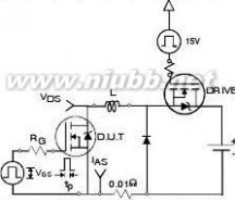
?? Limited by TJmax, starting TJ = 25°C, L = 4.8mH RG = 25?, IAS = 3.0A, VGS =10V.
Part not recommended for use above this value.?? Pulse width ≤ 1.0ms; duty cycle ≤ 2%.
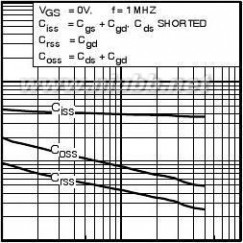
?? Coss eff. is a fixed capacitance that gives the same
charging time as Coss while VDS is rising from 0 to 80% VDSS.
??Limited by TJmax , see Fig.12a, 12b, 15, 16 for typical
repetitive avalanche performance.
??This value determined from sample failure population.100% tested to this value in production.
??When mounted on 1 inch square copper board.??When mounted on FR-4 board using minimumrecommended footprint.
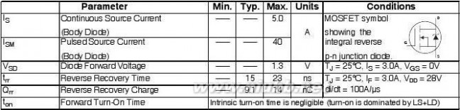
2www.irf.com
024 IRLL024Z中文资料

元器件交易网www.cecb2b.com
0.1
1
10
100
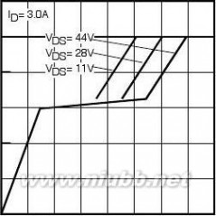
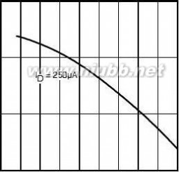
VDS, Drain-to-Source Voltage (V)Fig 1. Typical Output Characteristics
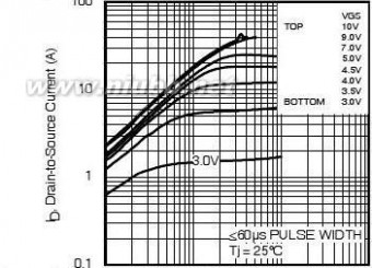

100
)
Α( tne
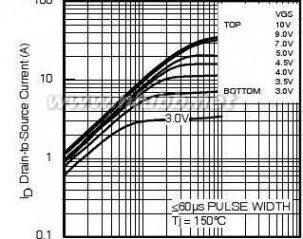
rru10
C ercuo-Sot-ni1
arD ,DI0.1
www.irf.comIRLL024Z
0.1
1
10
100
VDS, Drain-to-Source Voltage (V)
Fig 2. Typical Output Characteristics
10
8
6
4
s2
f00
2
4
6
8
10
12
ID,Drain-to-Source Current (A)
Fig 4. Typical Forward Transconductance
vs. Drain Current
3
G, Forward Transconductanc(S)
024 IRLL024Z中文资料

元器件交易网www.cecb2b.com
IRLL024Z
10000
)
Fp1000
(ecnaticapaC ,C100
10
1
10
100
VDS, Drain-to-Source Voltage (V)Fig 5. Typical Capacitance vs.
Drain-to-Source Voltage
10010
1
DS046.0
)
5.0(V egatlo4.0 Vecruo3.0-Sot-eta2.0G ,SVG1.00.0
012345678
QG Total Gate Charge (nC)
Fig 6. Typical Gate Charge vs.
Gate-to-Source Voltage
1000)
100(A

tne10
rruC ec1ruo-So0.1
t-niarD0.01
,D0.001
I0.0001
0.1
1.0
10
100
1000.0
VDS, Drain-to-Source Voltage (V)
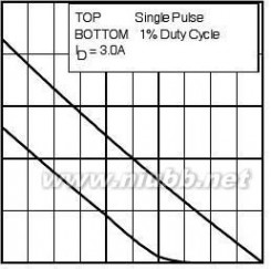
Fig 8. Maximum Safe Operating Area
www.irf.com
I, Reverse Drain Current (A)
扩展:z0607中文资料 / mke02z64vqh2中文资料 / ds1302z中文资料
024 IRLL024Z中文资料
元器件交易网www.cecb2b.com
IRLL024Z
RDS(on) , Drain-to-Source On Resistance (Normalized)
5
4
ID, Drain Current (A

)
3
2
1
025
50
75
100
125
150
TA , Ambient Temperature (°C)
TJ , Junction Temperature (°C)
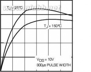
Fig 9. Maximum Drain Current vs.
Ambient Temperature
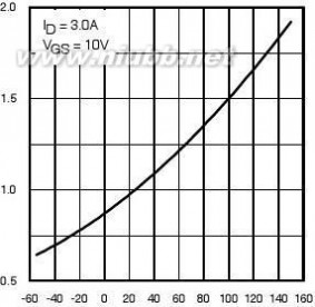
Fig 10. Normalized On-Resistance
vs. Temperature
t1 , Rectangular Pulse Duration (sec)
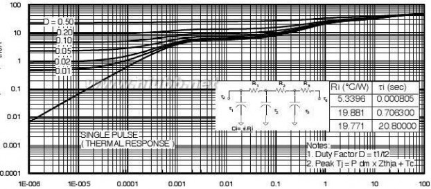
Fig 11. Maximum Effective Transient Thermal Impedance, Junction-to-Ambient
www.irf.com5
024 IRLL024Z中文资料

元器件交易网www.cecb2b.com
IRLL024Z
100
VDD
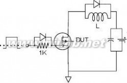
Fig 12a. Unclamped Inductive Test Circuit

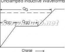
IVFig 13a. Basic Gate Charge Waveform
Fig 13b. Gate Charge Test Circuit
6

)
Jm( ygre80
nE ehcna60
lavA eslu40
P el
gniS 20
, SAE025
50
75
100
125
150
Starting TJ , Junction Temperature (°C)
Fig 12c. Maximum Avalanche Energy
vs. Drain Current
2.5
2.0
1.5
)ht(SG1.0
-75
-50
-25
25
50
75
100
125
150
TJ , Temperature ( °C )
Fig 14. Threshold Voltage vs. Temperature
www.irf.com
V
Gate threshold Voltage (V)
024 IRLL024Z中文资料

元器件交易网www.cecb2b.com
IRLL024Z
Avalanche Current (A
)
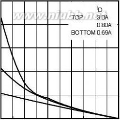
tav (sec)
Fig 15. Typical Avalanche Current vs.Pulsewidth
25
EAR , Avalanche Energy (mJ)
20
15
10
5
025
50
75
100
125
150
Starting TJ , Junction Temperature (°C)
Notes on Repetitive Avalanche Curves , Figures 15, 16:(For further info, see AN-1005 at www.irf.com)1. Avalanche failures assumption:
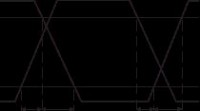
Purely a thermal phenomenon and failure occurs at a temperature far in excess of Tjmax. This is validated for every part type.
2. Safe operation in Avalanche is allowed as long asTjmax is not exceeded.
3. Equation below based on circuit and waveforms shown in Figures 12a, 12b.
4. PD (ave) = Average power dissipation per single avalanche pulse.
5. BV = Rated breakdown voltage (1.3 factor accounts for voltage increase during avalanche).6. Iav = Allowable avalanche current.
7. ?T = Allowable rise in junction temperature, not to exceed Tjmax (assumed as 25°C in Figure 15, 16). tav = Average time in avalanche. D = Duty cycle in avalanche = tav ·f
ZthJC(D, tav) = Transient thermal resistance, see figure 11)
PD (ave) = 1/2 ( 1.3·BV·Iav) = DT/ ZthJC
Iav = 2DT/ [1.3·BV·Zth]EAS (AR) = PD (ave)·tav
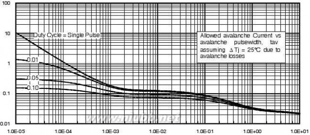
Fig 16. Maximum Avalanche Energy
vs. Temperature
www.irf.com7
024 IRLL024Z中文资料

元器件交易网www.cecb2b.com
IRLL024Z
* VGS = 5V for Logic Level Devices
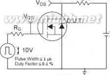
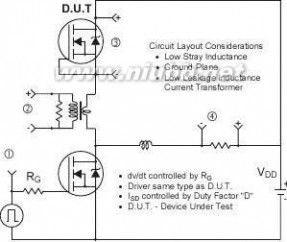
Fig 17. Peak Diode Recovery dv/dt Test Circuit for N-Channel
HEXFET? Power MOSFETs

扩展:z0607中文资料 / mke02z64vqh2中文资料 / ds1302z中文资料
VDD
Fig 18a. Switching Time Test Circuit
VVd(on)
r
d(off)
f
Fig 18b. Switching Time Waveforms
8www.irf.com
024 IRLL024Z中文资料

元器件交易网www.cecb2b.com
IRLL024Z
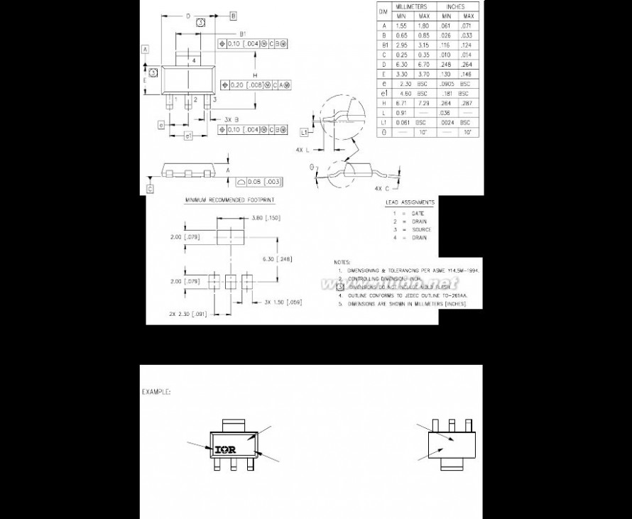
SOT-223 (TO-261AA) Package Outline
Dimensions are shown in milimeters (inches)
024 IRLL024Z中文资料
Dimensions are shown in milimeters (inches)
4.10 (.161)3.90 (.154)
1.85 (.072)1.65 (.065)
0.35 (.013)0.25 (.010)
TR
2.05 (.080)1.95 (.077)
7.55 (.297)7.45 (.294)
7.60 (.299)7.40 (.292)
1.60 (.062)1.50 (.059) TYP.
FEED DIRECTION
12.10 (.475)11.90 (.469)
7.10 (.279)6.90 (.272)
16.30 (.641)15.70 (.619)
2.30 (.090)2.10 (.083)
NOTES :
1. CONTROLLING DIMENSION: MILLIMETER.2. OUTLINE CONFORMS TO EIA-481 & EIA-541.
13.20 (.519)12.80 (.504)
15.40 (.607)11.90 (.469)
330.00(13.000) MAX.
50.00 (1.969) MIN.
NOTES :
1. OUTLINE COMFORMS TO EIA-418-1.
2. CONTROLLING DIMENSION: MILLIMETER..18.40 (.724) MAX.
14.40 (.566)12.40 (.488)
Data and specifications subject to change without notice.
This product has been designed for the Automotive [Q101] market.

Qualification Standards can be found on IR’s Web site.
IR WORLD HEADQUARTERS: 233 Kansas St., El Segundo, California 90245, USA Tel: (310) 252-7105
TAC Fax: (310) 252-7903
Visit us at www.irf.com for sales contact information. 08/04
10www.irf.com
扩展:z0607中文资料 / mke02z64vqh2中文资料 / ds1302z中文资料
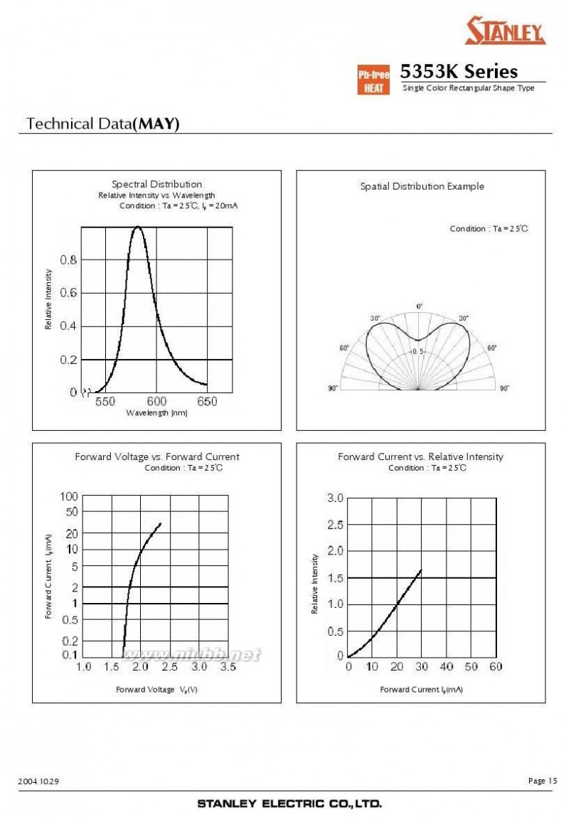
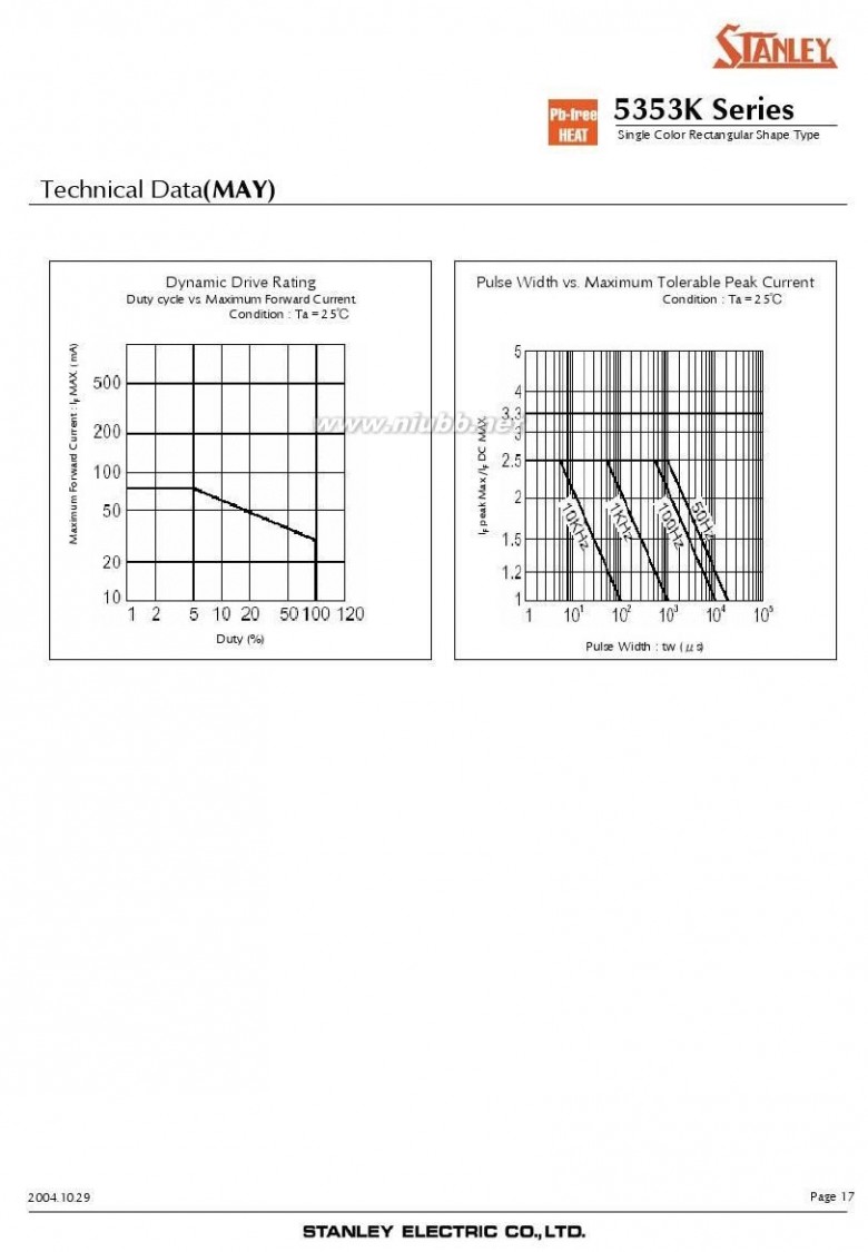
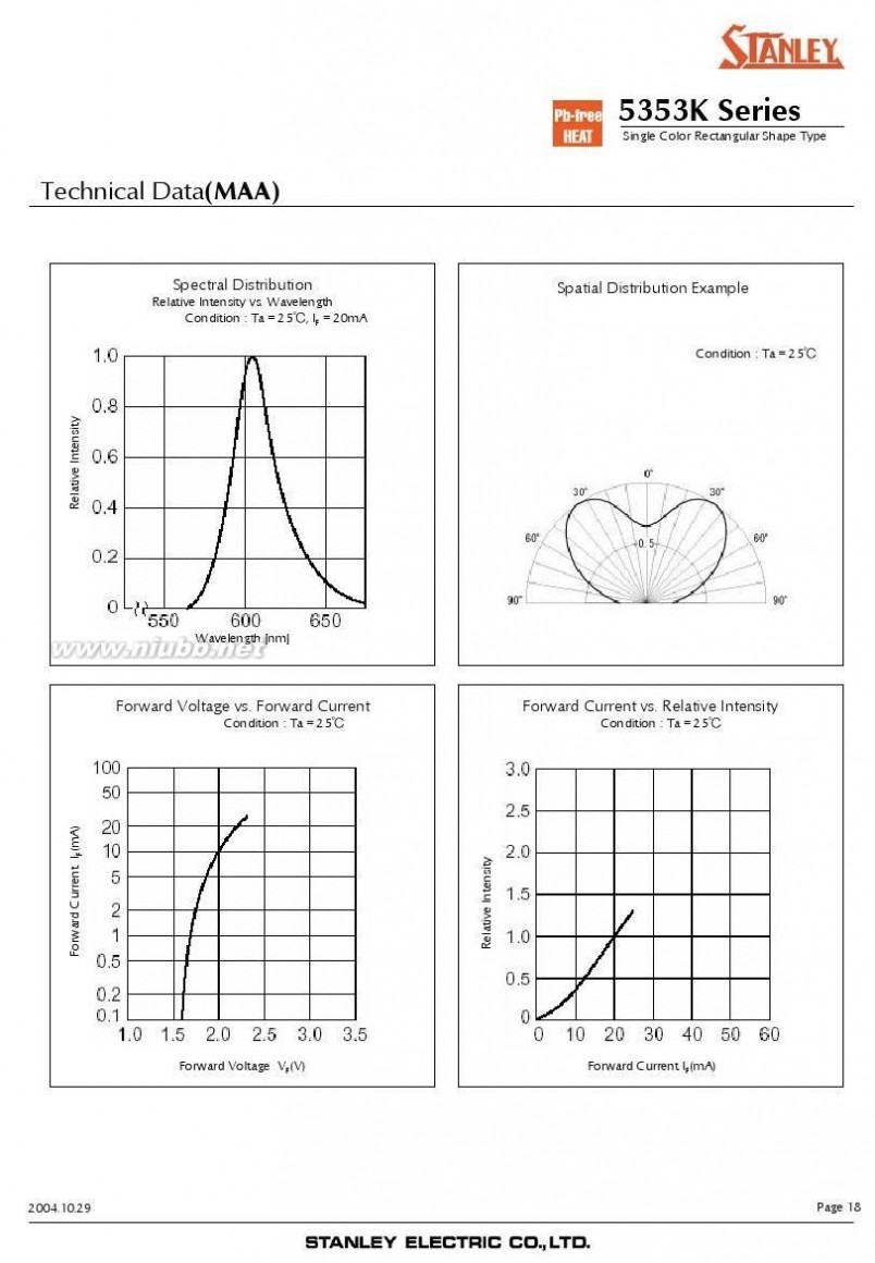
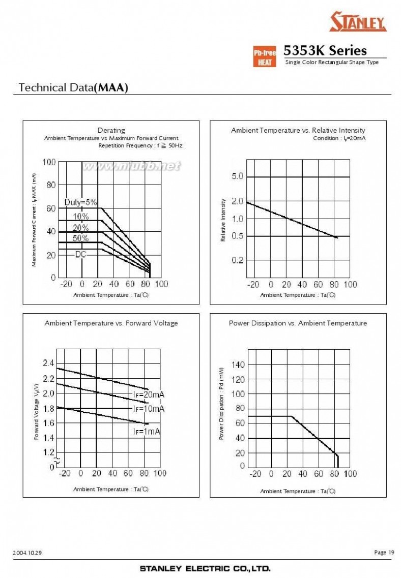
三 : MAY5353K中文资料
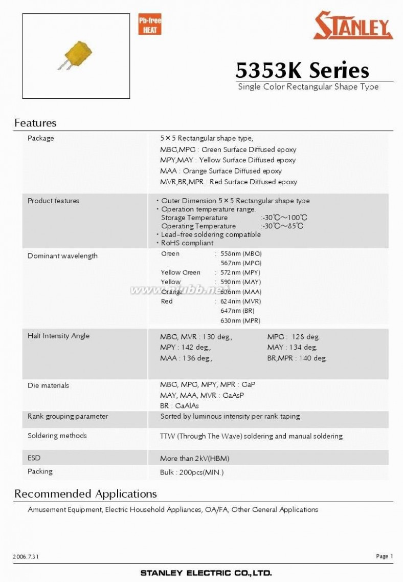
元器件交易网www.cecb2b.com
5353k MAY5353K中文资料
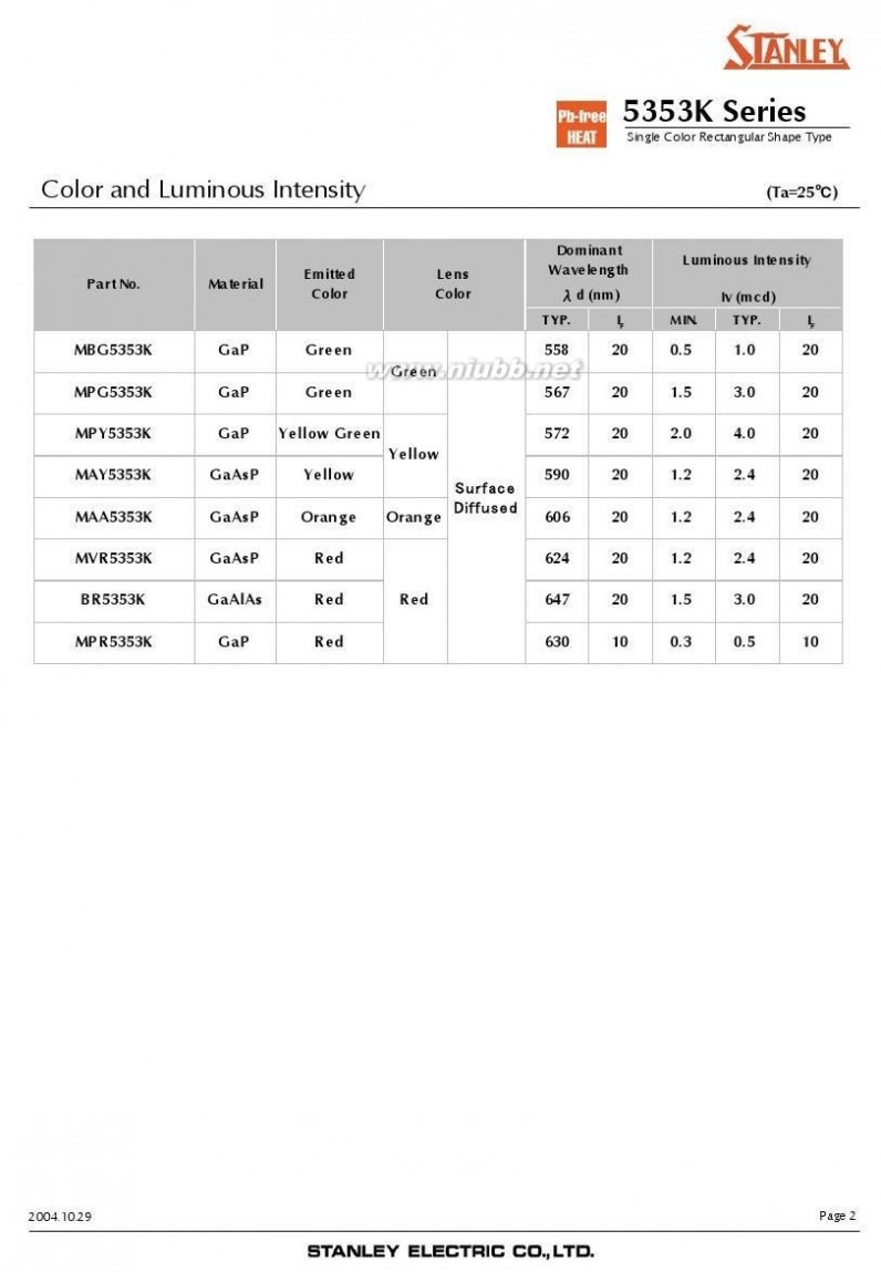
元器件交易网www.cecb2b.com
5353k MAY5353K中文资料
元器件交易网www.cecb2b.com
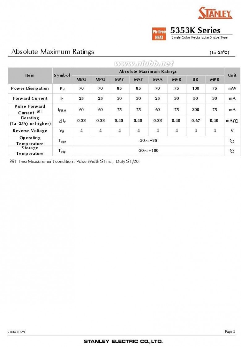
5353k MAY5353K中文资料
元器件交易网www.cecb2b.com
5353k MAY5353K中文资料
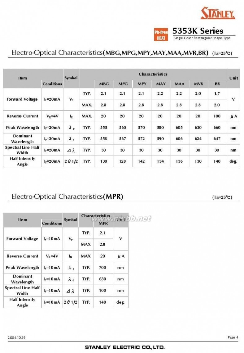
元器件交易网www.cecb2b.com
5353k MAY5353K中文资料
元器件交易网www.cecb2b.com
5353k MAY5353K中文资料
元器件交易网www.cecb2b.com
5353k MAY5353K中文资料
元器件交易网www.cecb2b.com
5353k MAY5353K中文资料
元器件交易网www.cecb2b.com
5353k MAY5353K中文资料
元器件交易网www.cecb2b.com
5353k MAY5353K中文资料
元器件交易网www.cecb2b.com
5353k MAY5353K中文资料

元器件交易网www.cecb2b.com
5353k MAY5353K中文资料
元器件交易网www.cecb2b.com
5353k MAY5353K中文资料

元器件交易网www.cecb2b.com
5353k MAY5353K中文资料
元器件交易网www.cecb2b.com
5353k MAY5353K中文资料

元器件交易网www.cecb2b.com
5353k MAY5353K中文资料
元器件交易网www.cecb2b.com
5353k MAY5353K中文资料
元器件交易网www.cecb2b.com
5353k MAY5353K中文资料
元器件交易网www.cecb2b.com
5353k MAY5353K中文资料
元器件交易网www.cecb2b.com
5353k MAY5353K中文资料
元器件交易网www.cecb2b.com
5353k MAY5353K中文资料
元器件交易网www.cecb2b.com
5353k MAY5353K中文资料

元器件交易网www.cecb2b.com
5353k MAY5353K中文资料

元器件交易网www.cecb2b.com
5353k MAY5353K中文资料
元器件交易网www.cecb2b.com
5353k MAY5353K中文资料
元器件交易网www.cecb2b.com
5353k MAY5353K中文资料
元器件交易网www.cecb2b.com
5353k MAY5353K中文资料
元器件交易网www.cecb2b.com
扩展:mb95f564k中文资料 / ta8428k中文资料 / k4s561632中文资料
5353k MAY5353K中文资料

元器件交易网www.cecb2b.com
5353k MAY5353K中文资料
元器件交易网www.cecb2b.com
5353k MAY5353K中文资料
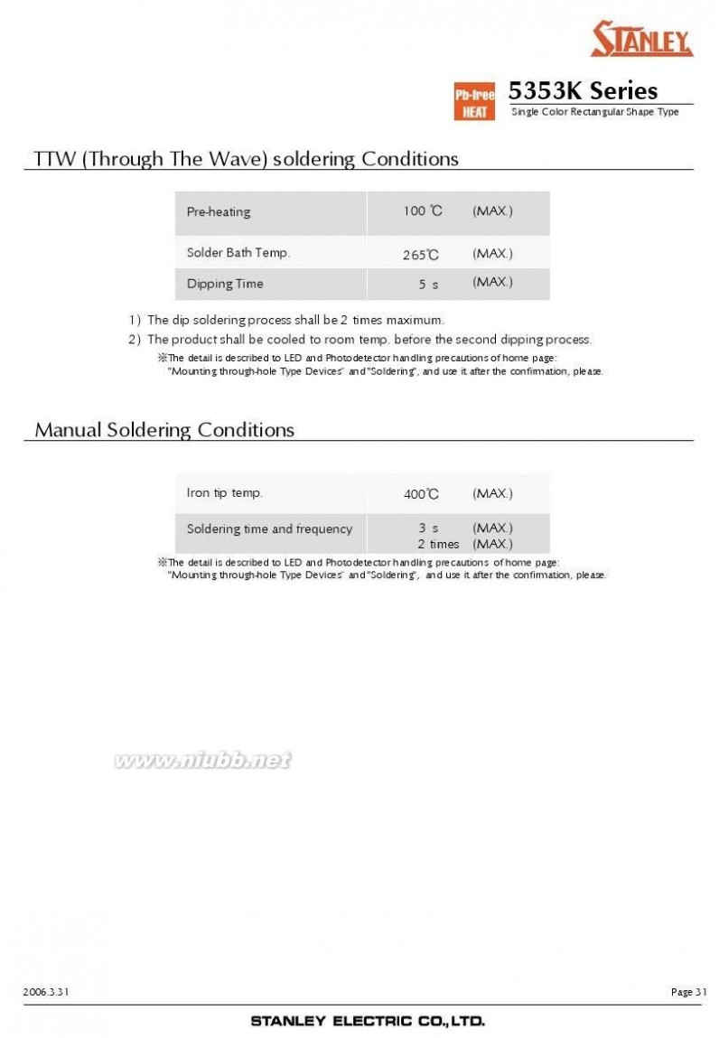
元器件交易网www.cecb2b.com
5353k MAY5353K中文资料
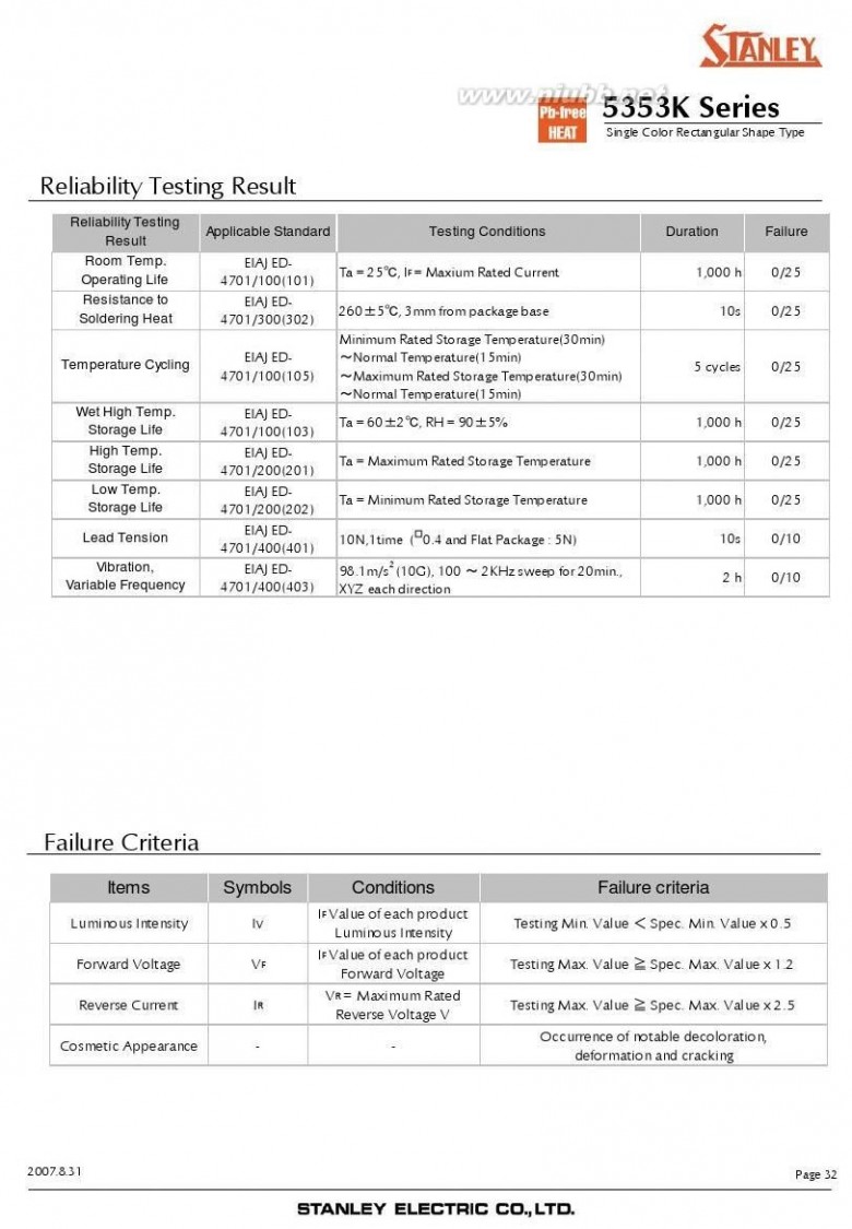
元器件交易网www.cecb2b.com
5353k MAY5353K中文资料
元器件交易网www.cecb2b.com
扩展:mb95f564k中文资料 / ta8428k中文资料 / k4s561632中文资料
本文标题:中文资料-MACH5中文资料61阅读| 精彩专题| 最新文章| 热门文章| 苏ICP备13036349号-1