一 : 94SVP685X0010A5中文资料

元器件交易网www.cecb2b.com
94SVP
Vishay OS-CON

Vertical Surface Mounting Capacitors
FEATURES
?New Vishay OS-CON series as results ofpolymerized organic semiconductor aselectrolyte
?Features superior heat-proof characteristicscompared with previously developed VishayOS-CON series
?Particularly effective when used as surface mountingdevices of the switching power supply
?Rated ripple current values are guaranteed at 105 °C
?No need to consider derating on maximum allowable ripple

current
Fig.1 Component outline
QUICK REFERENCE DATA
DESCRIPTION
Operating Temperature RangeCapacitance Tolerance at 120 Hz
Tangent of Loss Angle (tan δ) at 120 HzLeakage Current (μA/2 minutes) (or less)*
Equivalent Series Resistance (Ω), (100 k to 300 kHz)Characteristics at high temp. and low temp.Impedance Ratio at 100 kHz, + 20 °C
VALUE
- 55 °C to + 105 °C
M: ± 20 %
Values in Standard Ratings TableValues in Standard Ratings TableValues in Standard Ratings Table
- 55 °C+ 105 °CΔC/Ctan δESR

Leakage Current
ΔC/Ctan δESR
Leakage Current
Z/Z20 °CZ/Z20 °C
1.0 to 1.250.75 to1.0
Within ± 20 % Endurance + 105 °C, 2000 hours
Rated Voltage Applied (25 WV to 20 V)≤ 1.5 x the value of Tangent of Loss Angle (1000 hours for A5/B6 sizes)≤ 1.5 x the value of ESR
≤ The Value of Leakage Current
Within ± 20 % Damp heat (Steady state)
≤ 1.5 x the value of Tangent of Loss Angle (+ 60 °C, 90 to 95 % RH, 1000 hours, no voltage)
≤ 1.5 x the value of ESR (500 hours for A5/B6 sizes)
≤ The Value of Leakage Current after Voltage
Reverse Voltage GuaranteeTemporary: < 20 % of the rated voltage
Continuous: < 10 % of the rated voltage
ΔC/CWithin ± 10 % Solder heat resistance (VPS)**
tan δ≤ 1.3 x the value of Tangent of Loss Angle(215 °C x 90 s) or (230 °C x 60 s)
ESR≤ 1.3 x the value of ESR (Please consult us for A5/B6 sizes)
Leakage Current≤ The Value of Leakage Current after Voltage
* If any doubt arises, measure the current after applying voltage (voltage treatment). Voltage Treatment: The rated voltage is applied to VishayOS-CON (2.5 to 20 WV) for 120 minutes at 105 °C. (However, 20 V is applied to a 25 WV Vishay OS-CON).** Refer to Standard Ratings table for soldering recommendation.
DIMENSIONS in millimeters
DIMENSIONS in millimeters
SIZECODEA5B6C6E7F8E12F12
?D ± 0.54.05.06.38.010.08.010.0
L max.5.56.06.07.08.012.012.7
W ± 0.2
H ± 0.2
C ± 0.2
R
P ± 0.21.01.42.13.24.63.24.6
4.34.35.00.5 to 0.85.35.36.00.5 to 0.86.60.5 to 0.80.5 to 0.8to 0.80.8 to 1.111.00.8 to 1.1
www.vishay.com
308
Document Number: 90021
Revision: 26-Jun-06
svp 94SVP685X0010A5中文资料
元器件交易网www.cecb2b.com
94SVP
Vertical Surface Mounting Capacitors

Vishay OS-CON
RECOMMENDED LAND PATTERN
DIMENSIONS in millimeters
SIZECODEA5B6C6E7F8E12F12
a1.01.42.12.84.32.84.3
b6.27.49.111.113.111.113.1
c1.61.61.61.91.91.91.9
CASE CODE LIST
46.310162025(5.2)(8.2)(11.5)(18.4)(23)(25)
3.3----A5--4.7---A5---6.8---A5--C610.0---A5-B6E715.0---A5B6--27.0-----C6-22.0--A5-B6C6F833.0-A5-B6-E7E1239.0-B6--C6--47.0--B6C6-E7-56.0---C6E7F8F1268.0-B6---F8-82.0--C6-E7--100.0--C6-F8E12-120.0---E7---150.0-C6, E7-E7, F8F8F12-180.0----E12--220.0--E7,F8----270.0---E7, F8---330.0-E7F8E12F12--470.0--F8,E12----560.0-E12-F12---680.0E12F8-----820.0--F12----1200.0-F12-----1500.0F12------*** WV = Rated Voltage. **** (SV) = Surge Voltage (at room temperature). The description contents are subject to chage due to technical
improvement without notice. Please ask for latest specifications for order and use.CAPACITANCE
(μF)
STANDARD RATINGS
CASE CODE
PART NUMBER*
RATED RATED MAX. ESR
(100 k to VOLTAGE CAPACITANCE
(V)(μF)300 kHz) (mΩ)
22 RIPPLE CURRENT
(mAmps)
at 100 kHz, + 105 °C
590 660 660 670 670 700 740
TANGENT CURRENT (μA) OF LOSS (After 2 ANGLEMinutes)
www.vishay.com
309
A5
* Part Numbers shown are for ± 20 % capacitance tolerance (X0).Document Number: 90021Revision: 26-Jun-06
svp 94SVP685X0010A5中文资料
元器件交易网www.cecb2b.com
94SVP
Vishay OS-CON

Vertical Surface Mounting Capacitors
STANDARD RATINGS
CASE CODE
PART NUMBER*
RATED RATED MAX. ESR VOLTAGE CAPACITANCE (100 k to
(V)(μF)300 kHz) (mΩ)
RIPPLE CURRENT
(mAmps)
at 100 kHz, + 105 °C
850 920 920 990 1060 1100 701100 1200 1390 6014501390 1450 1510 40181050 1570 1620 1500 1700 1700 1800 1890 2120 3525602350 2560 2560 2000 2200 2200 2400 2670 2670 3020 3020 2537003300 3700 30 2980 25 3260 22 3480 19 3740 17 3960 4080 16 4080 28 3800 21 4220 17 4580 15 4870 14 5040 135230135230
TANGENT CURRENT (μA) OF LOSS (After 2 ANGLEMinutes)13685 88 10894 126103 300277592413 400 576 660 592 448340 700 600 792 840 775 960750
B6
47 6827C6
10082 E7
150220F8
47033 E12
470 680 56 F12
820 12001500
* Part Numbers shown are for ± 20 % capacitance tolerance (X0).
www.vishay.com310
Document Number: 90021
Revision: 26-Jun-06
svp 94SVP685X0010A5中文资料

元器件交易网www.cecb2b.com
Legal Disclaimer NoticeVishay
Notice
Specifications of the products displayed herein are subject to change without notice. Vishay Intertechnology, Inc.,or anyone on its behalf, assumes no responsibility or liability for any errors or inaccuracies.
Information contained herein is intended to provide a product description only. No license, express or implied, byestoppel or otherwise, to any intellectual property rights is granted by this document. Except as provided in Vishay'sterms and conditions of sale for such products, Vishay assumes no liability whatsoever, and disclaims any expressor implied warranty, relating to sale and/or use of Vishay products including liability or warranties relating to fitnessfor a particular purpose, merchantability, or infringement of any patent, copyright, or other intellectual property right.The products shown herein are not designed for use in medical, life-saving, or life-sustaining applications.Customers using or selling these products for use in such applications do so at their own risk and agree to fullyindemnify Vishay for any damages resulting from such improper use or sale.
Document Number: 91000
Revision: 08-Apr-05www.vishay.com1
二 : M95160-W中文资料
元器件交易网www.cecb2b.com
M95160
M95080
16 Kbit and 8 Kbit serial SPI bus EEPROM
with high speed clock
Features
■Compatible with SPI bus serial interface
(positive clock SPI modes)
Single supply voltage:
–4.5 V to 5.5 V for M95xxx
–2.5 V to 5.5 V for M95xxx-W
–1.8 V to 5.5 V for M95xxx-R
High Speed: 10 MHz
Status Register
Hardware Protection of the Status Register
Byte and page write (up to 32 bytes)
Self-timed programming cycle
Adjustable size read-only EEPROM area
Enhanced ESD protection
More than 1 million Erase/Write cycles
More than 40-year data retention
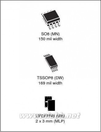
Packages
–ECOPACK? (RoHS compliant)
Device summary
Part number
M95160
M95160M95160-W
M95160-R
M95080
M95080M95080-W
M95080-R■■■■■■■■■■■Table 1.
Reference
May 2007 Rev 61/45
www.st.com
95160 M95160-W中文资料
元器件交易网www.cecb2b.com
ContentsM95160, M95080Contents
1
2Description . . . . . . . . . . . . . . . . . . . . . . . . . . . . . . . . . . . . . . . . . . . . . . . . . 6Signal description . . . . . . . . . . . . . . . . . . . . . . . . . . . . . . . . . . . . . . . . . . . 8
2.1
2.2
2.3
2.4
2.5
2.6
2.7
2.8Serial Data Output (Q) . . . . . . . . . . . . . . . . . . . . . . . . . . . . . . . . . . . . . . . . 8Serial Data Input (D) . . . . . . . . . . . . . . . . . . . . . . . . . . . . . . . . . . . . . . . . . 8Serial Clock (C) . . . . . . . . . . . . . . . . . . . . . . . . . . . . . . . . . . . . . . . . . . . . . 8889VCC supply voltage . . . . . . . . . . . . . . . . . . . . . . . . . . . . . . . . . . . . . . . . . . . 9VSS ground . . . . . . . . . . . . . . . . . . . . . . . . . . . . . . . . . . . . . . . . . . . . . . . . . 9
3Connecting to the SPI bus . . . . . . . . . . . . . . . . . . . . . . . . . . . . . . . . . . . 10
3.1SPI modes . . . . . . . . . . . . . . . . . . . . . . . . . . . . . . . . . . . . . . . . . . . . . . . . 11
4Operating features . . . . . . . . . . . . . . . . . . . . . . . . . . . . . . . . . . . . . . . . . 12
4.1Supply voltage (VCC) . . . . . . . . . . . . . . . . . . . . . . . . . . . . . . . . . . . . . . . . 12
4.1.1
4.1.2
4.1.3
4.1.4Operating supply voltage VCC . . . . . . . . . . . . . . . . . . . . . . . . . . . . . . . . . . . . . . . . .12Power-up conditions . . . . . . . . . . . . . . . . . . . . . . . . . . . . . . . . . . . . . . . 12Power-up and device reset . . . . . . . . . . . . . . . . . . . . . . . . . . . . . . . . . . 12Power-down . . . . . . . . . . . . . . . . . . . . . . . . . . . . . . . . . . . . . . . . . . . . . . 13
4.2
4.3
4.4
4.5Active Power and Standby Power Modes . . . . . . . . . . . . . . . . . . . . . . . . . 13Hold condition . . . . . . . . . . . . . . . . . . . . . . . . . . . . . . . . . . . . . . . . . . . . . . 13Status Register . . . . . . . . . . . . . . . . . . . . . . . . . . . . . . . . . . . . . . . . . . . . . 13Data protection and protocol control . . . . . . . . . . . . . . . . . . . . . . . . . . . . 14
5
6Memory organization . . . . . . . . . . . . . . . . . . . . . . . . . . . . . . . . . . . . . . . 15Instructions . . . . . . . . . . . . . . . . . . . . . . . . . . . . . . . . . . . . . . . . . . . . . . . 16
6.1
6.2
6.3Write Enable (WREN) . . . . . . . . . . . . . . . . . . . . . . . . . . . . . . . . . . . . . . . 16Write Disable (WRDI) . . . . . . . . . . . . . . . . . . . . . . . . . . . . . . . . . . . . . . . . 17Read Status Register (RDSR) . . . . . . . . . . . . . . . . . . . . . . . . . . . . . . . . . 18
6.3.1WIP bit . . . . . . . . . . . . . . . . . . . . . . . . . . . . . . . . . . . . . . . . . . . . . . . . . . 18
2/45
95160 M95160-W中文资料
元器件交易网www.cecb2b.com
M95160, M950806.3.2
6.3.3
6.3.4ContentsWEL bit . . . . . . . . . . . . . . . . . . . . . . . . . . . . . . . . . . . . . . . . . . . . . . . . . 18BP1, BP0 bits . . . . . . . . . . . . . . . . . . . . . . . . . . . . . . . . . . . . . . . . . . . . . 18SRWD bit . . . . . . . . . . . . . . . . . . . . . . . . . . . . . . . . . . . . . . . . . . . . . . . . 18
6.4
6.5
6.6Write Status Register (WRSR) . . . . . . . . . . . . . . . . . . . . . . . . . . . . . . . . . 20Read from Memory Array (READ) . . . . . . . . . . . . . . . . . . . . . . . . . . . . . . 23Write to Memory Array (WRITE) . . . . . . . . . . . . . . . . . . . . . . . . . . . . . . . 24
7Delivery state . . . . . . . . . . . . . . . . . . . . . . . . . . . . . . . . . . . . . . . . . . . . . . 26
7.1Initial delivery state . . . . . . . . . . . . . . . . . . . . . . . . . . . . . . . . . . . . . . . . . . 26
扩展:m95160 / stc15f104w中文资料 / w25x40 中文资料
8
9
10
11
12Maximum rating . . . . . . . . . . . . . . . . . . . . . . . . . . . . . . . . . . . . . . . . . . . . 26DC and AC parameters . . . . . . . . . . . . . . . . . . . . . . . . . . . . . . . . . . . . . . 27Package mechanical . . . . . . . . . . . . . . . . . . . . . . . . . . . . . . . . . . . . . . . . 38Part numbering . . . . . . . . . . . . . . . . . . . . . . . . . . . . . . . . . . . . . . . . . . . . 41Revision history . . . . . . . . . . . . . . . . . . . . . . . . . . . . . . . . . . . . . . . . . . . 43
3/45
95160 M95160-W中文资料
元器件交易网www.cecb2b.com
List of tablesM95160, M95080List of tables
Table 1.
Table 2.
Table 3.
Table 4.
Table 5.
Table 6.
Table 7.
Table 8.
Table 9.
Table 10.
Table 11.
Table 12.
Table 13.
Table 14.
Table 15.
Table 16.
Table 17.
Table 18.
Table 19.
Table 20.
Table 21.
Table 22.
Table 23.
Table 24.
Table 25.
Table 26.
Table 27.
Table 28.
Table 29.
Table 30.Device summary. . . . . . . . . . . . . . . . . . . . . . . . . . . . . . . . . . . . . . . . . . . . . . . . . . . . . . . . . . 1Signal names . . . . . . . . . . . . . . . . . . . . . . . . . . . . . . . . . . . . . . . . . . . . . . . . . . . . . . . . . . . . 6Write-Protected block size . . . . . . . . . . . . . . . . . . . . . . . . . . . . . . . . . . . . . . . . . . . . . . . . . 14Instruction set. . . . . . . . . . . . . . . . . . . . . . . . . . . . . . . . . . . . . . . . . . . . . . . . . . . . . . . . . . . 16Status Register format . . . . . . . . . . . . . . . . . . . . . . . . . . . . . . . . . . . . . . . . . . . . . . . . . . . . 18Protection modes . . . . . . . . . . . . . . . . . . . . . . . . . . . . . . . . . . . . . . . . . . . . . . . . . . . . . . . . 21Address range bits . . . . . . . . . . . . . . . . . . . . . . . . . . . . . . . . . . . . . . . . . . . . . . . . . . . . . . . 22Absolute maximum ratings. . . . . . . . . . . . . . . . . . . . . . . . . . . . . . . . . . . . . . . . . . . . . . . . . 26Operating conditions (M95160 and M95080). . . . . . . . . . . . . . . . . . . . . . . . . . . . . . . . . . . 27Operating conditions (M95160-W and M95080-W) . . . . . . . . . . . . . . . . . . . . . . . . . . . . . . 27Operating conditions (M95160-R and M95080-R) . . . . . . . . . . . . . . . . . . . . . . . . . . . . . . . 27AC measurement conditions. . . . . . . . . . . . . . . . . . . . . . . . . . . . . . . . . . . . . . . . . . . . . . . . 27Capacitance . . . . . . . . . . . . . . . . . . . . . . . . . . . . . . . . . . . . . . . . . . . . . . . . . . . . . . . . . . . . 28DC characteristics (M95160 and M95080, device grade 3) . . . . . . . . . . . . . . . . . . . . . . . . 28DC characteristics (M95160 and M95080, device grade 6) . . . . . . . . . . . . . . . . . . . . . . . . 28DC characteristics (M95160-W and M95080-W, device grade 3). . . . . . . . . . . . . . . . . . . . 29DC characteristics (M95160-W and M95080-W, device grade 6). . . . . . . . . . . . . . . . . . . . 29DC characteristics (M95160-R and M95080-R) . . . . . . . . . . . . . . . . . . . . . . . . . . . . . . . . . 30AC characteristics (M95160 and M95080, device grade 3) . . . . . . . . . . . . . . . . . . . . . . . . 31AC characteristics (M95160 and M95080, device grade 6) . . . . . . . . . . . . . . . . . . . . . . . . 32AC characteristics (M95160-W and M95080-W, device grade 3). . . . . . . . . . . . . . . . . . . . 33AC characteristics (M95160-W and M95080-W, device grade 6). . . . . . . . . . . . . . . . . . . . 34AC characteristics (M95160-R and M95080-R) . . . . . . . . . . . . . . . . . . . . . . . . . . . . . . . . . 35SO8 narrow – 8 lead Plastic Small Outline, 150 mils body width,mechanical data . . . . . . . . . . . . . . . . . . . . . . . . . . . . . . . . . . . . . . . . . . . . . . . . . . . . . . . . . 38UFDFPN8 (MLP8) 8-lead Ultra thin Fine pitch Dual Flat Package No lead2 x 3 mm, package mechanical data . . . . . . . . . . . . . . . . . . . . . . . . . . . . . . . . . . . . . . . . . 39TSSOP8 – 8 lead Thin Shrink Small Outline, package mechanical data . . . . . . . . . . . . . . 40Ordering information scheme. . . . . . . . . . . . . . . . . . . . . . . . . . . . . . . . . . . . . . . . . . . . . . . 41Available M95160 products (package, voltage range, temperature grade) . . . . . . . . . . . . 42Available M95080 products (package, voltage range, temperature grade) . . . . . . . . . . . . 42Document revision history . . . . . . . . . . . . . . . . . . . . . . . . . . . . . . . . . . . . . . . . . . . . . . . . . 434/45
95160 M95160-W中文资料
元器件交易网www.cecb2b.com
M95160, M95080List of figuresList of figures
Figure 1.
Figure 2.
Figure 3.
Figure 4.
Figure 5.
Figure 6.
Figure 7.
扩展:m95160 / stc15f104w中文资料 / w25x40 中文资料
Figure 8.
Figure 9.
Figure 10.
Figure 11.
Figure 12.
Figure 13.
Figure 14.
Figure 15.
Figure 16.
Figure 17.
Figure 18.
Figure 19.
Figure 20.Packages . . . . . . . . . . . . . . . . . . . . . . . . . . . . . . . . . . . . . . . . . . . . . . . . . . . . . . . . . . . . . . . 1Logic diagram. . . . . . . . . . . . . . . . . . . . . . . . . . . . . . . . . . . . . . . . . . . . . . . . . . . . . . . . . . . . 68-pin package connections (top view) . . . . . . . . . . . . . . . . . . . . . . . . . . . . . . . . . . . . . . . . . 7Bus master and memory devices on the SPI bus. . . . . . . . . . . . . . . . . . . . . . . . . . . . . . . . 10SPI modes supported. . . . . . . . . . . . . . . . . . . . . . . . . . . . . . . . . . . . . . . . . . . . . . . . . . . . . 11Block diagram. . . . . . . . . . . . . . . . . . . . . . . . . . . . . . . . . . . . . . . . . . . . . . . . . . . . . . . . . . . 15Write Enable (WREN) sequence . . . . . . . . . . . . . . . . . . . . . . . . . . . . . . . . . . . . . . . . . . . . 16Write Disable (WRDI) sequence. . . . . . . . . . . . . . . . . . . . . . . . . . . . . . . . . . . . . . . . . . . . . 17Read Status Register (RDSR) sequence. . . . . . . . . . . . . . . . . . . . . . . . . . . . . . . . . . . . . . 19Write Status Register (WRSR) sequence. . . . . . . . . . . . . . . . . . . . . . . . . . . . . . . . . . . . . . 22Read from Memory Array (READ) sequence . . . . . . . . . . . . . . . . . . . . . . . . . . . . . . . . . . . 23Byte Write (WRITE) sequence . . . . . . . . . . . . . . . . . . . . . . . . . . . . . . . . . . . . . . . . . . . . . . 24Page Write (WRITE) sequence . . . . . . . . . . . . . . . . . . . . . . . . . . . . . . . . . . . . . . . . . . . . . 25AC measurement I/O waveform. . . . . . . . . . . . . . . . . . . . . . . . . . . . . . . . . . . . . . . . . . . . . 27Serial input timing. . . . . . . . . . . . . . . . . . . . . . . . . . . . . . . . . . . . . . . . . . . . . . . . . . . . . . . . 36Hold timing . . . . . . . . . . . . . . . . . . . . . . . . . . . . . . . . . . . . . . . . . . . . . . . . . . . . . . . . . . . . . 36Output timing . . . . . . . . . . . . . . . . . . . . . . . . . . . . . . . . . . . . . . . . . . . . . . . . . . . . . . . . . . . 37SO8 narrow – 8 lead Plastic Small Outline, 150 mils body width, package outline . . . . . . 38UFDFPN8 (MLP8) 8-lead Ultra thin Fine pitch Dual Flat Package No lead2 x 3 mm2, package outline. . . . . . . . . . . . . . . . . . . . . . . . . . . . . . . . . . . . . . . . . . . . . . . . . 39TSSOP8 – 8 lead Thin Shrink Small Outline, package outline. . . . . . . . . . . . . . . . . . . . . . 40
5/45
95160 M95160-W中文资料
元器件交易网www.cecb2b.com
DescriptionM95160, M95080
1 Description
These electrically erasable programmable memory (EEPROM) devices are accessed by a high speed SPI-compatible bus. The memory array is organized as 2048 x 8 bit (M95160), and 1024 x 8 bit (M95080).
The device is accessed by a simple serial interface that is SPI-compatible. The bus signals are C, D and Q, as shown in Table 2. and Figure 2.
In order to meet environmental requirements, ST offers the M95xxx in ECOPACK? packages. ECOPACK? packages are Lead-free and RoHS compliant.
ECOPACK is an ST trademark. ECOPACK specifications are available at: www.st.com.
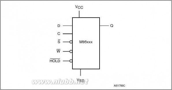
Table 2.
Signal names
Function
Serial ClockSerial Data inputSerial Data outputChip SelectWrite Protect
InputInputOutputInputInputInput
Direction
Signal nameCDQVCCVSS
Supply voltageGround
6/45
95160 M95160-W中文资料
元器件交易网www.cecb2b.com
M95160, M95080Description1.See Package mechanical section for package dimensions, and how to identify pin-1.
7/45

95160 M95160-W中文资料
元器件交易网www.cecb2b.com
Signal descriptionM95160, M950802 Signal description
During all operations, VCC must be held stable and within the specified valid range:
VCC(min) to VCC(max).
All of the input and output signals must be held High or Low (according to voltages of VIH,
VOH, VIL or VOL, as specified in Table 13. to Table 18.). These signals are described next.
2.1 Serial Data Output (Q)
This output signal is used to transfer data serially out of the device. Data is shifted out on the
falling edge of Serial Clock (C).
2.2 Serial Data Input (D)
This input signal is used to transfer data serially into the device. It receives instructions,
addresses, and the data to be written. Values are latched on the rising edge of Serial Clock
(C).
2.3 Serial Clock (C)
扩展:m95160 / stc15f104w中文资料 / w25x40 中文资料
This input signal provides the timing of the serial interface. Instructions, addresses, or data
present at Serial Data Input (D) are latched on the rising edge of Serial Clock (C). Data on Serial Data Output (Q) changes after the falling edge of Serial Clock (C).
2.4 When this input signal is High, the device is deselected and Serial Data Output (Q) is at high
impedance. Unless an internal Write cycle is in progress, the device will be in the Standby mode.
instruction.
deselecting the device.During the Hold condition, the Serial Data Output (Q) is high impedance, and Serial Data
Input (D) and Serial Clock (C) are Don’t Care.
8/45
95160 M95160-W中文资料
元器件交易网www.cecb2b.com
M95160, M95080Signal description
2.6 The main purpose of this input signal is to freeze the size of the area of memory that is
protected against Write instructions (as specified by the values in the BP1 and BP0 bits of
the Status Register).
This pin must be driven either High or Low, and must be stable during all write instructions.
2.7 VCC supply voltage
VCC is the supply voltage.
2.8 VSS ground
VSS is the reference for the VCC supply voltage.
9/45
95160 M95160-W中文资料
元器件交易网www.cecb2b.com
Connecting to the SPI busM95160, M95080
3 Connecting to the SPI bus
These devices are fully compatible with the SPI protocol.
All instructions, addresses and input data bytes are shifted in to the device, most significant bit first. The Serial Data Input (D) is sampled on the first rising edge of the Serial Clock (C) All output data bytes are shifted out of the device, most significant bit first. The Serial Data Output (Q) is latched on the first falling edge of the Serial Clock (C) after the instruction (such as the Read from Memory Array and Read Status Register instructions) have been clocked into the device.
Figure 4. shows three devices, connected to an MCU, on an SPI bus. Only one device is selected at a time, so only one device drives the Serial Data Output (Q) line at a time, all the others being high impedance.
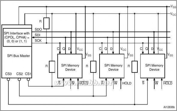
1.Figure4 shows an example of three memory devices connected to an MCU, on an SPI bus. Only one memory device is selected at a time, so only one memory device drives the Serial Data Output (Q) line at a time, the other memory devices are high impedance.
The pull-up resistor R (represented in Figure4) ensures that a device is not selected if the In applications where the Bus Master may be in a state where all input/output SPI buses are high impedance at the same time (for example, if the Bus Master is reset during the transmission of an instruction), the clock line (C) must be connected to an external pull-down resistor so that, if all inputs/outputs become high impedance, the C line is pulled Low time, and so, that the tSHCH requirement is met. The typical value of R is 100 k?.
10/45
95160 M95160-W中文资料
元器件交易网www.cecb2b.com
M95160, M95080Connecting to the SPI bus
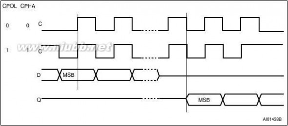
3.1 SPI modes
These devices can be driven by a microcontroller with its SPI peripheral running in either of
the two following modes:
●
●CPOL=0, CPHA=0CPOL=1, CPHA=1
For these two modes, input data is latched in on the rising edge of Serial Clock (C), and
output data is available from the falling edge of Serial Clock (C).
The difference between the two modes, as shown in Figure 5., is the clock polarity when the
bus master is in Stand-by mode and not transferring data:
●
●C remains at 0 for (CPOL=0, CPHA=0)C remains at 1 for (CPOL=1, CPHA=1)
11/45
95160 M95160-W中文资料
元器件交易网www.cecb2b.com
Operating featuresM95160, M950804 Operating features
4.1
4.1.1 Supply voltage (VCC)Operating supply voltage VCC
Prior to selecting the memory and issuing instructions to it, a valid and stable VCC voltage
within the specified [VCC(min), VCC(max)] range must be applied (see Table9, Table10 and
Table11). In order to secure a stable dc supply voltage, it is recommended to decouple the
VCC line with a suitable capacitor (usually of the order of 10 nF to 100 nF) close to the
VCC/VSS package pins.
This voltage must remain stable and valid until the end of the transmission of the instruction
and, for a Write instruction, until the completion of the internal write cycle (tW).
4.1.2 Power-up conditions
When the power supply is turned on, VCC rises from VSS to VCC. During this time, the Chip
CC voltage, it is therefore
CC via a suitable pull-up resistor.sensitive as well as level sensitive: after power-up, the device does not become selected The VCC rise time must not vary faster than 1 V/μs.
扩展:m95160 / stc15f104w中文资料 / w25x40 中文资料
4.1.3 Power-up and device reset
In order to prevent inadvertent Write operations during power-up, a power on reset (POR)
circuit is included. At power-up (continuous rise of VCC), the device does not respond to any
instruction until VCC has reached the power on reset threshold voltage (this threshold is
lower than the minimum VCC operating voltage defined in Table9, Table10 and Table11).
Once VCC has passed the POR threshold, the device is reset and is in the following state:
●●
●Standby Power modedeselected (at next power-up, a falling edge is required on Chip Select (S) before any instructions can be started)not in the Hold condition
the Write Enable Latch (WEL) is reset to 0
Write In Progress (WIP) is reset to 0. The SRWD, BP1 and BP0 bits of the Status
Register are unchanged from the previous power-down (they are non-volatile bits).Status Register state:●●
12/45
95160 M95160-W中文资料
元器件交易网www.cecb2b.com
M95160, M95080Operating features
4.1.4 Power-down
At Power-down (continuous decrease of VCC), as soon as VCC drops from the normal
operating voltage to below the power on reset threshold voltage, the device stops
responding to any instruction sent to it.
During Power-down, the device must be deselected and in Standby Power mode (that is follow the voltage applied on VCC.
4.2 Active Power and Standby Power Modesdevice consumes ICC, as specified in Table 13. to Table 18.progress, the device then goes into the Standby Power mode, and the device consumption
drops to ICC1.
4.3 Hold conditionresetting the clocking sequence.
During the Hold condition, the Serial Data Output (Q) is high impedance, and Serial Data
Input (D) and Serial Clock (C) are Don’t Care.Normally, the device is kept selected, for the whole duration of the Hold condition.
Deselecting the device while it is in the Hold condition, has the effect of resetting the state of
the device, and this mechanism can be used if it is required to reset any processes that had
been in progress.Serial Clock (C) already being Low.Serial Clock (C) already being Low.
4.4 Status Register
Figure 6. shows the position of the Status Register in the control logic of the device. The
Status Register contains a number of status and control bits that can be read or set (as
appropriate) by specific instructions. See Section6.3: Read Status Register (RDSR) for a
detailed description of the Status Register bits
13/45
95160 M95160-W中文资料
元器件交易网www.cecb2b.com
Operating featuresM95160, M95080
4.5 Data protection and protocol control
Non-volatile memory devices can be used in environments that are particularly noisy, and within applications that could experience problems if memory bytes are corrupted. Consequently, the device features the following data protection mechanisms:
●●
Write and Write Status Register instructions are checked that they consist of a number of clock pulses that is a multiple of eight, before they are accepted for execution.All instructions that modify data must be preceded by a Write Enable (WREN)
instruction to set the Write Enable Latch (WEL) bit. This bit is returned to its reset state by the following events:––––
Power-up
Write Disable (WRDI) instruction completionWrite Status Register (WRSR) instruction completionWrite (WRITE) instruction completion
●●
The Block Protect (BP1, BP0) bits in the Status Register allow part of the memory to be configured as read-only.
Register to be protected.
the rising edge of Serial Clock (C) for the last bit of the instruction, and before the next rising edge of Serial Clock (C).
Two points need to be noted in the previous sentence:
●
The ‘last bit of the instruction’ can be the eighth bit of the instruction code, or the eighth bit of a data byte, depending on the instruction (except for Read Status Register (RDSR) and Read (READ) instructions).
The ‘next rising edge of Serial Clock (C)’ might (or might not) be the next bus transaction for some other device on the SPI bus.
Write-Protected block size
Array Addresses ProtectedM95160none0600h - 07FFh0400h - 07FFh0000h - 07FFh
M95080
none 0300h - 03FFh 0200h - 03FFh 0000h - 03FFh
●
Table 3.
Status Register Bits
Protected Block
0 1 1
1 0 1
Upper quarter Upper half Whole memory
14/45
95160 M95160-W中文资料
元器件交易网www.cecb2b.com
M95160, M95080Memory organization
5 Memory organization
The memory is organized as shown in Figure 6.

15/45
95160 M95160-W中文资料
扩展:m95160 / stc15f104w中文资料 / w25x40 中文资料
元器件交易网www.cecb2b.com
InstructionsM95160, M950806 Instructions
Each instruction starts with a single-byte code, as summarized in Table 4.
If an invalid instruction is sent (one not contained in Table 4.), the device automatically
deselects itself.
Table 4. Instruction set
DescriptionInstruction Format
0000 0110
0000 0100
0000 0101
0000 0001
0000 0011
0000 0010InstructionEnableDisableRDSR WRSR READ WRITE Read Status Register Write Status Register Read from Memory ArrayWrite to Memory Array
6.1 Write Enable (WREN)
The Write Enable Latch (WEL) bit must be set prior to each WRITE and WRSR instruction.
The only way to do this is to send a Write Enable instruction to the device.As shown in Figure 7.and the bits of the instruction byte are shifted in, on Serial Data Input (D). The device then
High.

16/45
95160 M95160-W中文资料
元器件交易网www.cecb2b.com
M95160, M95080Instructions
6.2 Write Disable (WRDI)
One way of resetting the Write Enable Latch (WEL) bit is to send a Write Disable instruction
to the device.
As shown in Figure 8.and the bits of the instruction byte are shifted in, on Serial Data Input (D).
The device then enters a wait state. It waits for a the device to be deselected, by Chip Select The Write Enable Latch (WEL) bit, in fact, becomes reset by any of the following events:
●
●
●
●Power-upWRDI instruction executionWRSR instruction completionWRITE instruction completion.
17/45
95160 M95160-W中文资料
元器件交易网www.cecb2b.com
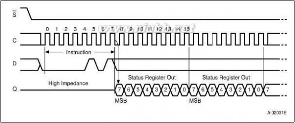
InstructionsM95160, M950806.3 Read Status Register (RDSR)
The Read Status Register (RDSR) instruction allows the Status Register to be read. The
Status Register may be read at any time, even while a Write or Write Status Register cycle
is in progress. When one of these cycles is in progress, it is recommended to check the
Write In Progress (WIP) bit before sending a new instruction to the device. It is also possible
to read the Status Register continuously, as shown in Figure 9.
The status and control bits of the Status Register are as follows:
6.3.1 WIP bit
The Write In Progress (WIP) bit indicates whether the memory is busy with a Write or Write
Status Register cycle. When set to 1, such a cycle is in progress, when reset to 0 no such
cycle is in progress.
6.3.2 WEL bit
The Write Enable Latch (WEL) bit indicates the status of the internal Write Enable Latch.
When set to 1 the internal Write Enable Latch is set, when set to 0 the internal Write Enable
Latch is reset and no Write or Write Status Register instruction is accepted.
6.3.3 BP1, BP0 bits
The Block Protect (BP1, BP0) bits are non-volatile. They define the size of the area to be
software protected against Write instructions. These bits are written with the Write Status
Register (WRSR) instruction. When one or both of the Block Protect (BP1, BP0) bits is set to
1, the relevant memory area (as defined in Table 5.) becomes protected against Write
(WRITE) instructions. The Block Protect (BP1, BP0) bits can be written provided that the
Hardware Protected mode has not been set.
6.3.4 SRWD bitThe Status Register Write Disable (SRWD) bit is operated in conjunction with the Write signal allow the device to be put in the Hardware Protected mode (when the Status Register
non-volatile bits of the Status Register (SRWD, BP1, BP0) become read-only bits and the
Write Status Register (WRSR) instruction is no longer accepted for execution.
Table 5.
b7
SRWD Status Register formatb0Status Register Write Protect
Block Protect Bits
Write Enable Latch Bit
Write In Progress Bit
18/45
95160 M95160-W中文资料
元器件交易网www.cecb2b.com
M95160, M95080Instructions 19/45
95160 M95160-W中文资料
元器件交易网www.cecb2b.com
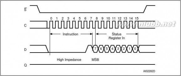
InstructionsM95160, M950806.4 Write Status Register (WRSR)
The Write Status Register (WRSR) instruction allows new values to be written to the Status
Register. Before it can be accepted, a Write Enable (WREN) instruction must previously have been executed. After the Write Enable (WREN) instruction has been decoded and
executed, the device sets the Write Enable Latch (WEL).followed by the instruction code and the data byte on Serial Data Input (D). The instruction is
timed Write cycle then starts, and continues for a period tW (as specified in Table19,
扩展:m95160 / stc15f104w中文资料 / w25x40 中文资料
Table20, Table21, Table22 and Table23), at the end of which the Write in Progress (WIP)
bit is reset to 0. The instruction sequence is shown in Figure 10.The Write Status Register (WRSR) instruction has no effect on b6, b5, b4, b1 and b0 of the
Status Register. b6, b5 and b4 are always read as 0.the eighth bit of the data byte, and before the next rising edge of Serial Clock (C). Otherwise,
driven High, the self-timed Write Status Register cycle (whose duration is tW) is initiated.
While the Write Status Register cycle is in progress, the Status Register may still be read to
check the value of the Write In Progress (WIP) bit. The Write In Progress (WIP) bit is 1
during the self-timed Write Status Register cycle, and is 0 when it is completed. When the
cycle is completed, the Write Enable Latch (WEL) is reset.
The Write Status Register (WRSR) instruction allows the user to change the values of the
Block Protect (BP1, BP0) bits, to define the size of the area that is to be treated as read-
only, as defined in Table 5.
The Write Status Register (WRSR) instruction also allows the user to set or reset the Status be put in the Hardware Protected Mode (HPM). The Write Status Register (WRSR)
instruction is not executed once the Hardware Protected Mode (HPM) is entered.
The contents of the Status Register Write Disable (SRWD) and Block Protect (BP1, BP0)
bits are frozen at their current values from just before the start of the execution of Write
Status Register (WRSR) instruction. The new, updated, values take effect at the moment of
completion of the execution of Write Status Register (WRSR) instruction.
20/45
95160 M95160-W中文资料
元器件交易网www.cecb2b.com
M95160, M95080Table 6.
Signal
1
0 InstructionsProtection modesSRWD Bit00ModeWrite Protection of the Status RegisterMemory contentProtected area(1)Unprotected area(1)
11Status Register is Writable (if the WREN Software instruction has set the Protected WEL bit)(SPM)The values in the BP1
and BP0 bits can be
changedWrite ProtectedReady to accept Write instructions
01Status Register is Hardware write Hardware protectedProtected Write ProtectedThe values in the BP1 (HPM)and BP0 bits cannot be
changedReady to accept Write instructions
1.As defined by the values in the Block Protect (BP1, BP0) bits of the Status Register, as shown in Table 6.The protection features of the device are summarized in Table 3.
When the Status Register Write Disable (SRWD) bit of the Status Register is 0 (its initial delivery state), it is possible to write to the Status Register provided that the Write Enable Latch (WEL) bit has previously been set by a Write Enable (WREN) instruction, regardless When the Status Register Write Disable (SRWD) bit of the Status Register is set to 1, two ●If Write Protect (W) is driven High, it is possible to write to the Status Register provided
that the Write Enable Latch (WEL) bit has previously been set by a Write Enable (WREN) instruction.
not possible to write to the Status Register even if the Write Enable Latch (WEL) bit has previously been set by a Write Enable (WREN) instruction. (Attempts to write to the Status Register are rejected, and are not accepted for execution). As a consequence, all the data bytes in the memory area that are
software protected (SPM) by the Block Protect (BP1, BP0) bits of the Status Register, are also hardware protected against data modification.●Regardless of the order of the two events, the Hardware Protected Mode (HPM) can be entered:
●●by setting the Status Register Write Disable (SRWD) bit after driving Write Protect (W) Low(SRWD) bit.
The only way to exit the Hardware Protected Mode (HPM) once entered is to pull Write never be activated, and only the Software Protected Mode (SPM), using the Block Protect (BP1, BP0) bits of the Status Register, can be used. 21/45
95160 M95160-W中文资料
元器件交易网www.cecb2b.com
InstructionsTable 7.
M95160, M95080Address range bits(1)
Device
Address BitsM95160A10-A0M95080A9-A0
1.b15 to b11 are Don’t Care on the M95160.b15 to b10 are Don’t Care on the M95080.
22/45
95160 M95160-W中文资料
元器件交易网www.cecb2b.com
M95160, M95080Instructions
6.5 Read from Memory Array (READ)
As shown in Figure 11.Low. The bits of the instruction byte and address bytes are then shifted in, on Serial Data
Input (D). The address is loaded into an internal address register, and the byte of data at
that address is shifted out, on Serial Data Output (Q).incremented, and the byte of data at the new address is shifted out.
When the highest address is reached, the address counter rolls over to zero, allowing the
扩展:m95160 / stc15f104w中文资料 / w25x40 中文资料
Read cycle to be continued indefinitely. The whole memory can, therefore, be read with a
single READ instruction.The first byte addressed can be any byte within any page.
The instruction is not accepted, and is not executed, if a Write cycle is currently in progress.
1.Depending on the memory size, as shown in Table 7., the most significant address bits are Don’t Care.
23/45
95160 M95160-W中文资料
元器件交易网www.cecb2b.com
InstructionsM95160, M950806.6 Write to Memory Array (WRITE)As shown in Figure 12.Low. The bits of the instruction byte, address byte, and at least one data byte are then
shifted in, on Serial Data Input (D).
data. In the case of Figure 12., this occurs after the eighth bit of the data byte has been
latched in, indicating that the instruction is being used to write a single byte. The self-timed
Write cycle starts, and continues for a period tWC (as specified in Table 20. to Table 23.), at
the end of which the Write in Progress (WIP) bit is reset to 0.
Figure 13., the next byte
of input data is shifted in, so that more than a single byte, starting from the given address
towards the end of the same page, can be written in a single internal Write cycle.
Each time a new data byte is shifted in, the least significant bits of the internal address
counter are incremented. If the number of data bytes sent to the device exceeds the page
boundary, the internal address counter rolls over to the beginning of the page, and the
previous data there are overwritten with the incoming data. (The page size of these devices
is 32 bytes).
The instruction is not accepted, and is not executed, under the following conditions:
●
●●
●if the Write Enable Latch (WEL) bit has not been set to 1 (by executing a Write Enable instruction just before)if a Write cycle is already in progressif the device has not been deselected, by Chip Select (S) being driven High, at a byte boundary (after the eighth bit, b0, of the last data byte that has been latched in)if the addressed page is in the region protected by the Block Protect (BP1 and BP0)
bits.
1.Depending on the memory size, as shown in Table 7., the most significant address bits are Don’t Care.
24/45
95160 M95160-W中文资料
元器件交易网www.cecb2b.com
M95160, M95080Instructions1.Depending on the memory size, as shown in Table 7., the most significant address bits are Don’t Care.
25/45
95160 M95160-W中文资料
元器件交易网www.cecb2b.com
Delivery stateM95160, M95080
7 Delivery state
7.1 Initial delivery state
The device is delivered with the memory array set at all 1s (FFh). The Status Register Write
Disable (SRWD) and Block Protect (BP1 and BP0) bits are initialized to 0.
8 Maximum rating
Stressing the device outside the ratings listed in Table 8. may cause permanent damage to
the device. These are stress ratings only, and operation of the device at these, or any other conditions outside those indicated in the Operating sections of this specification, is not implied. Exposure to Absolute Maximum Rating conditions for extended periods may affect device reliability. Refer also to the STMicroelectronics SURE Program and other relevant quality documents.Table 8.
SymbolTATSTGTLEADVOVIVCCVESD
Absolute maximum ratings
Parameter
Ambient operating temperatureStorage temperature
Lead temperature during solderingOutput voltageInput voltageSupply voltage
Electrostatic discharge voltage (human body model)(2)
Min.–40–65
Max.130150
°C°CVVVVUnit
See note(1)–0.50–0.50–0.50–4000
VCC+0.66.56.54000
1.Compliant with JEDEC Std J-STD-020C (for small body, Sn-Pb or Pb assembly), the ST ECOPACK?
7191395 specification, and the European directive on Restrictions on Hazardous Substances (RoHS) 2002/95/EU2.AEC-Q100-002 (compliant with JEDEC Std JESD22-A114A, C1=100 pF, R1=1500 ?, R2=500 ?)
26/45
95160 M95160-W中文资料
元器件交易网www.cecb2b.com
M95160, M95080DC and AC parameters
9 DC and AC parameters
This section summarizes the operating and measurement conditions, and the dc and ac characteristics of the device. The parameters in the dc and ac characteristic tables that follow are derived from tests performed under the measurement conditions summarized in the relevant tables. Designers should check that the operating conditions in their circuit match the measurement conditions when relying on the quoted parameters.Table 9.
扩展:m95160 / stc15f104w中文资料 / w25x40 中文资料
SymbolVCCTA
Supply voltage
Ambient operating temperature (device grade 6)Ambient operating temperature (device grade 3)
Operating conditions (M95160 and M95080)
Parameter
Min.4.5–40–40
Max.5.585125
UnitV°C°C
Table 10.
SymbolVCCTA
Operating conditions (M95160-W and M95080-W)
Parameter
Supply voltage
Ambient operating temperature (device grade 6)Ambient operating temperature (device grade 3)
Min.2.5–40–40
Max.5.585125
UnitV°C°C
Table 11.
SymbolVCCTA
Operating conditions (M95160-R and M95080-R)
Parameter
Supply voltage
Ambient operating temperature
Min.(1)1.8–40
Max.(1)5.585
UnitV°C
1.This product is under development. For more information, please contact your nearest ST sales office.
Table 12.
SymbolCL

AC measurement conditions(1)
Parameter
Load capacitanceInput rise and fall timesInput pulse voltages
Input and output timing reference voltages
Min.
Typ.30
50
0.2VCC to 0.8VCC0.3VCC to 0.7VCC
Max.
UnitpFnsVV
1.Output Hi-Z is defined as the point where data out is no longer driven.
27/45
95160 M95160-W中文资料
元器件交易网www.cecb2b.com
DC and AC parameters
Table 13.
SymbolCOUTCIN
M95160, M95080
Capacitance(1)
Parameter
Test conditionVOUT = 0 VVIN = 0 VVIN = 0 V
Min.
886Max.
pFpFpFUnit
Output capacitance (Q)Input capacitance (D)Input capacitance (other pins)
1.Sampled only, not 100% tested, at TA = 25 °C and a frequency of 5 MHz.
Table 14.
SymbolILIILOICCICC1VILVIHVOL (1)VOH (1)
DC characteristics (M95160 and M95080, device grade 3)
ParameterInput leakage currentOutput leakage currentSupply currentSupply current (Standby)Input low voltageInput high voltageOutput low voltageOutput high voltage
IOL = 2 mA, VCC = 5 VIOH = –2 mA, VCC = 5 V
0.8VCC
Test condition
VIN = VSS or VCC
CC, VOUT = VSS or VCCC=0.1VCC/0.9VCC at 5 MHz,VCC=5 V, Q=openCC, VCC = 5 V,VIN = VSS or VCC
–0.450.7VCCMin.
Max.± 2± 2350.3VCCVCC+10.4
UnitμAμAmAμAVVVV
1.For all 5 V range devices, the device meets the output requirements for both TTL and CMOS standards.
Table 15.
SymbolILIILOICCICC1VILVIHVOL(1)VOH (1)
DC characteristics (M95160 and M95080, device grade 6)
ParameterInput leakage currentOutput leakage currentSupply currentSupply current(Standby)Input low voltageInput high voltage
Output low voltageIOL = 2mA, VCC = 5 VOutput high voltage
IOH = –2mA, VCC = 5 V
0.8VCC
Test condition
VIN = VSS or VCC
CC, VOUT = VSS or VCCC=0.1VCC/0.9VCC at 10 MHz,VCC=5 V, Q=openCC, VCC = 5 V,VIN = VSS or VCC
–0.450.7VCCMin.
Max.± 2± 2520.3VCCVCC+10.4
UnitμAμAmAμAVVVV
1.For all 5 V range devices, the device meets the output requirements for both TTL and CMOS standards.
28/45
95160 M95160-W中文资料
元器件交易网www.cecb2b.com
M95160, M95080
Table 16.
SymbolILIILOICCICC1VILVIHVOLVOH
DC and AC parameters
DC characteristics (M95160-W and M95080-W, device grade 3)
ParameterInput leakage currentOutput leakage currentSupply currentSupply current (Standby)Input low voltageInput high voltageOutput low voltage
IOL = 1.5 mA, VCC = 2.5 V
0.8VCC
Test condition
VIN = VSS or VCC
CC, VOUT = VSS or VCCC=0.1VCC/0.9VCC at 5 MHz,VCC=2.5 V, Q=open
CC, VCC = 2.5 V, VIN = VSS or VCC
–0.450.7VCCMin.
Max.± 2± 2220.3VCCVCC+10.4
UnitμAμAmAμAVVVV
Output high voltageIOH = –0.4 mA, VCC = 2.5 V
Table 17.
SymbolILIILO
DC characteristics (M95160-W and M95080-W, device grade 6)
ParameterInput leakage currentOutput leakage current
Test condition
VIN = VSS or VCC
CC, VOUT = VSS or VCCC=0.1VCC/0.9VCC at 5 MHz,
VCC=2.5V, Q=open, Process SA
Min.
Max.± 2± 22
UnitμAμAmA
ICC
Supply current
C=0.1VCC/0.9VCC at 10 MHz,
VCC=2.5 V, Q=open, Process GB or SB
CC, 2.5 V <VCC < 5.5 VVIN = VSS or VCC
–0.450.7VCC
IOL = 1.5 mA, VCC = 2.5 V
0.8VCC
5mA
ICC1VILVIHVOLVOH
Supply current(Standby)Input low voltageInput high voltageOutput low voltage
20.3VCCVCC+10.4
μAVVVV
Output high voltageIOH = –0.4 mA, VCC = 2.5 V
29/45
95160 M95160-W中文资料
元器件交易网www.cecb2b.com
DC and AC parameters
Table 18.
SymbolILIILOICCICC1VILVIHVOLVOH
M95160, M95080
DC characteristics (M95160-R and M95080-R)
Parameter
Test Condition
VIN = VSS or VCC
扩展:m95160 / stc15f104w中文资料 / w25x40 中文资料
CC, VOUT = VSS or VCCC=0.1VCC/0.9VCC at 5 MHz,VCC=1.8V, Q=openCC, VIN = VSS or VCC,1.8 < VCC < 2.5 V
–0.450.7VCC
IOL = 0.15mA, VCC = 1.8VIOH = –0.1mA, VCC= 1.8V
0.8VCCMin.
Max.± 2± 2310.3VCCVCC+10.3
UnitμAμAmAμAVVVV
Input leakage currentOutput leakage currentSupply currentSupply current (Standby)Input low voltageInput high voltageOutput low voltageOutput high voltage
30/45
95160 M95160-W中文资料
元器件交易网www.cecb2b.com
M95160, M95080
Table 19.
DC and AC parameters
AC characteristics (M95160 and M95080, device grade 3)
Test conditions specified in Table 12. and Table 9.
SymbolfCtSLCHtSHCHtSHSLtCHSHtCHSLtCH(1)tCL (1))tCLCH (2)tCHCL (2)tDVCHtCHDXtHHCHtHLCHtCLHLtCLHHtSHQZ(2)tCLQVtCLQXtQLQH(2)tQHQL(2)tHHQVtHLQZ(2)tW
Alt.fSCKtCSS1tCSS2tCStCSH
Clock frequency
ParameterMin.D.C.909010090909090
Max.5
UnitMHznsnsnsnsnsnsns
tCLHtCLLtRCtFCtDSUtDH
Clock high timeClock low timeClock rise timeClock fall timeData in setup timeData in hold time
11
2030704000
10060
5050501005
μsμsnsnsnsnsnsnsnsnsnsnsnsnsnsms
tDIStVtHOtROtFOtLZtHZtWC
Output disable timeClock low to output validOutput hold timeOutput rise timeOutput fall time
Write time
1.tCH + tCL must never be lower than the shortest possible clock period, 1/fC(max).2.Value guaranteed by characterization, not 100% tested in production.
31/45
95160 M95160-W中文资料
元器件交易网www.cecb2b.com
DC and AC parameters
Table 20.
M95160, M95080
AC characteristics (M95160 and M95080, device grade 6)
Test conditions specified in Table 12. and Table 9.
SymbolfCtSLCHtSHCHtSHSLtCHSHtCHSLtCH(1)tCL (1)tCLCH(2)tCHCL(2)tDVCHtCHDXtHHCHtHLCHtCLHLtCLHHtSHQZ(2)tCLQVtCLQXtQLQH(2)tQHQL(2)tHHQVtHLQZ ((2))
tW
Alt.fSCKtCSS1tCSS2tCStCSH
Clock frequency
ParameterMin.D.C.15154025154040
Max.10
UnitMHznsnsnsnsnsnsns
tCLHtCLLtRCtFCtDSUtDH
Clock high timeClock low timeClock rise timeClock fall timeData in setup timeData in hold time
11
1515152000
2535
202025355
μsμsnsnsnsnsnsnsnsnsnsnsnsnsnsms
tDIStVtHOtROtFOtLZtHZtWC
Output disable timeClock low to output validOutput hold timeOutput rise timeOutput Fall Time
Write Time
1.tCH + tCL must never be lower than the shortest possible clock period, 1/fC(max).2.Value guaranteed by characterization, not 100% tested in production.
32/45
95160 M95160-W中文资料
元器件交易网www.cecb2b.com
M95160, M95080
Table 21.
DC and AC parameters
AC characteristics (M95160-W and M95080-W, device grade 3)
Test conditions specified in Table 12. and Table 10.
SymbolfCtSLCHtSHCHtSHSLtCHSHtCHSLtCH(1)tCL(1)tCLCH(2)tCHCL(2)tDVCHtCHDXtHHCHtHLCHtCLHLtCLHHtSHQZ(2)tCLQVtCLQXtQLQH(2)tQHQL(2)tHHQVtHLQZ(2)tW
Alt.fSCKtCSS1tCSS2tCStCSH
Clock frequencyParameterMin.D.C.909010090909090
Max.5
UnitMHznsnsnsnsnsnsns
tCLHtCLLtRCtFCtDSUtDH
Clock high timeClock low timeClock rise timeClock fall timeData in setup timeData in hold time
11
2030704000
10060
5050501005
μsμsnsnsnsnsnsnsnsnsnsnsnsnsnsms
tDIStVtHOtROtFOtLZtHZtWC
Output disable timeClock low to output validOutput hold timeOutput rise timeOutput fall time
Write time
1.tCH + tCL must never be lower than the shortest possible clock period, 1/fC(max).2.Value guaranteed by characterization, not 100% tested in production.
33/45
95160 M95160-W中文资料
元器件交易网www.cecb2b.com
DC and AC parameters
Table 22.
M95160, M95080
AC characteristics (M95160-W and M95080-W, device grade 6)
Test conditions specified in Table 12. and Table 10.
Process SA
Process GB or SB (1)
Unit
Min.
Max.5
Min.D.C.30304030304040
11
2030704000
10060
5050501005
404040405
1010303000
404022Max.10
MHznsnsnsnsnsnsnsμsμsnsnsnsnsnsnsnsnsnsnsnsnsnsms
D.C.909010090909090
SymbolfCtSLCHtSHCHtSHSLtCHSHtCHSLtCH(2)tCL (2)tCLCH(3)tCHCL(3)tDVCHtCHDXtHHCHtHLCHtCLHLtCLHHtSHQZ(3)tCLQVtCLQXtQLQH(3)tQHQL(3)tHHQVtHLQZ(3)tW
Alt.Parameter
fSCKClock frequencytCSS1tCSS2tCS
tCSHtCLHtCLLtRCtFC
Clock high timeClock low timeClock rise timeClock fall time
tDSUData in setup timetDH
Data in hold timeClock low hold time after Clock low hold time after Clock low set-up time before Clock low set-up time before tDIStVtHOtROtFOtLZtHZtWC
Output disable timeClock low to output validOutput hold timeOutput rise timeOutput fall time
Write time
1.Preliminary data
2.tCH + tCL must never be lower than the shortest possible clock period, 1/fC(max).3.Value guaranteed by characterization, not 100% tested in production.
扩展:m95160 / stc15f104w中文资料 / w25x40 中文资料
34/45
95160 M95160-W中文资料
元器件交易网www.cecb2b.com
M95160, M95080
Table 23.
DC and AC parameters
AC characteristics (M95160-R and M95080-R)
Test conditions specified in Table 12. and Table 11.
SymbolfCtSLCHtSHCHtSHSLtCHSHtCHSLtCH(1)tCL(1)tCLCH(2)tCHCL(2)tDVCHtCHDXtHHCHtHLCHtCLHLtCLHHtSHQZ(2)tCLQVtCLQXtQLQH(2)tQHQL(2)tHHQVtHLQZ(2)tW
Alt.
fSCKClock frequencytCSS1ParameterMin.D.C.60609060608080
Max.5
UnitMHznsnsnsnsnsnsns
tCSS2tCS
tCSHtCLHClock high timetCLLClock low timetRCtFC
Clock rise timeClock fall time
22
2020606000
8080
808080805
μsμsnsnsnsns00nsnsnsnsnsnsnsms
tDSUData in setup timetDH
Data in hold time
tDIStVtHOtROtFOtLZtHZtWC
Output disable timeClock low to output validOutput hold timeOutput rise timeOutput fall time
Write time
1.tCH + tCL must never be lower than the shortest possible clock period, 1/fC(max).2.Value guaranteed by characterization, not 100% tested in production.
35/45
95160 M95160-W中文资料
元器件交易网www.cecb2b.com
DC and AC parameters
M95160, M95080
36/45
95160 M95160-W中文资料
元器件交易网www.cecb2b.com
M95160, M95080DC and AC parameters 37/45
95160 M95160-W中文资料
元器件交易网www.cecb2b.com
Package mechanicalM95160, M95080
10 Package mechanical
Figure 18.SO8 narrow – 8 lead Plastic Small Outline, 150 mils body width, package
1.Drawing is not to scale.
Table 24.
SO8 narrow – 8 lead Plastic Small Outline, 150 mils body width,mechanical data
millimeters
inches
Max1.75
0.101.250.280.17
0.480.230.10
4.906.003.901.27
4.805.803.80–0.250°0.40
1.04
5.006.204.00–0.508°1.27
0.0410.1930.2360.1540.050
0.1890.2280.150–0.0100°0.016
0.25
0.0040.0490.0110.007
0.0190.0090.0040.1970.2440.157–0.0208°0.050
Typ
Min
Max0.0690.010
Symbol
Typ
AA1A2bccccDEE1ehkLL1
Min
38/45
95160 M95160-W中文资料
元器件交易网www.cecb2b.com
M95160, M95080Package mechanical
Figure 19.UFDFPN8 (MLP8) 8-lead Ultra thin Fine pitch Dual Flat Package No lead
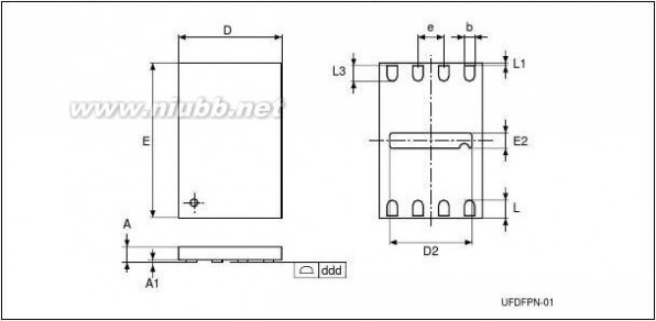
1.Drawing is not to scale.
2.The central pad (the area E2 by D2 in the above illustration) is pulled, internally, to VSS. It must not be
allowed to be connected to any other voltage or signal line on the PCB, for example during the soldering process.
Table 25.
UFDFPN8 (MLP8) 8-lead Ultra thin Fine pitch Dual Flat Package No lead2 x 3 mm, package mechanical data
millimeters
inches
Max0.600.050.302.101.700.08
3.000.200.500.45
2.900.10–0.40
3.100.30–0.500.15
0.30
0.012
0.1180.0080.0200.018
0.1140.004–0.016
Typ0.0220.0010.0100.0790.063
Min0.0200.0000.0080.0750.059
Max0.0240.0020.0120.0830.0670.0030.1220.012–0.0200.006
Symbol
Typ
AA1bDD2dddEE2eLL1L3
0.550.020.252.001.60
0.500.000.201.901.50
Min
39/45
95160 M95160-W中文资料
元器件交易网www.cecb2b.com
Package mechanicalM95160, M95080
1.Drawing is not to scale.
Table 26.
Symbol
TSSOP8 – 8 lead Thin Shrink Small Outline, package mechanical data
millimeters
Typ
Min
Max1.200
0.050
1.000
0.8000.1900.090
0.1501.0500.3000.2000.100
3.0000.6506.4004.4000.6001.000
0°8
8°
2.900–6.2004.3000.450
3.100–6.6004.5000.750
0.11810.02560.25200.17320.02360.0394
0°8
8°
0.1142–0.24410.16930.0177
0.0394
0.00200.03150.00750.0035
Typ
inchesMin
Max0.04720.00590.04130.01180.00790.00390.1220–0.25980.17720.0295
AA1A2bcCPDeEE1LL1αN
40/45
95160 M95160-W中文资料
元器件交易网www.cecb2b.com
M95160, M95080Part numbering11 Part numbering
Table 27.
Example:
Device type
Device function
080 = 8 Kbit (1024 x 8)
Operating voltage
CCW = VCC = 2.5 to 5.5 V
R = VCC = 1.8 to 5.5 V
Package
DW = TSSOP8
MB = MLP8 (UFDFPN8)
扩展:m95160 / stc15f104w中文资料 / w25x40 中文资料
Device grade
6 = Industrial temperature range, –40 to 85 °C.
Device tested with standard test flow
3 = Device tested with High Reliability Certified Flow(1).
Automotive temperature range (–40 to 125 °C)
Option
blank = Standard Packing
T = Tape and Reel Packing
Plating technology
G or P = ECOPACK? (RoHS compliant)
Process(2)
1.ST strongly recommends the use of the Automotive Grade devices for use in an automotive environment. The High Reliability Certified Flow (HRCF) is described in the quality note QNEE9801. Please ask your nearest ST sales office for a copy.
2.The Process letter (/G or /S) applies only to Range 3 devices. For Range 6 devices, the process letters do not appear in the Ordering Information but only appear on the device package (marking) and on the shipment box. Please contact your nearest ST Sales Office. For more information on how to identify products by the Process Identification Letter, please refer to AN2043: Serial EEPROM Device Marking. Ordering information schemeM95160–WMN6TP/SFor a list of available options (speed, package, etc.) or for further information on any aspect
of this device, please contact your nearest ST Sales Office.
The category of second Level Interconnect is marked on the package and on the inner box
label, in compliance with JEDEC Standard JESD97. The maximum ratings related to
soldering conditions are also marked on the inner box label.
41/45
95160 M95160-W中文资料
元器件交易网www.cecb2b.com
Part numbering
Table 28.
M95160, M95080
Available M95160 products (package, voltage range, temperature grade)
M951604.5 V to 5.5 VRange 6Range3NA(1)NA(1)
M95160-W2.5 V to 5.5 VRange 6Range3Range 6Range3NA(1)
M95160-R1.8 V to 5.5 VRange 6Range 6Range 6
PackageSO8 (MN)TSSOP (DW)MLP 2x3mm (MB)
1.NA = Not available
Table 29.
Available M95080 products (package, voltage range, temperature grade)
M950804.5 V to 5.5 VRange 6Range3NA(1)NA(1)
M95080-W2.5 V to 5.5 VRange 6Range3Range 6Range3Range 6
M95080-R1.8 V to 5.5 VRange 6Range 6Range 6
PackageSO8 (MN)TSSOP (DW)MLP 2x3mm (MB)
1.NA = Not available
42/45
95160 M95160-W中文资料
元器件交易网www.cecb2b.com
M95160, M95080Revision history12 Revision history
Table 30.
Date
19-Jul-2001
06-Feb-2002
18-Oct-2002
04-Nov-2002
13-Nov-2002
21-Nov-2003 Document revision historyRevision1.01.11.21.31.42.0ChangesDocument written from previous M95640/320/160/080 datasheetAnnouncement made of planned upgrade to 10MHz clock for the 5V, –40 to 85°C, rangeTSSOP8 (3x3mm body size, MSOP8) package addedNew products, identified by the process letter W, addedCorrection to footnote in Ordering Information tableTable of contents, and Pb-free options added. VIL(min) improved to –
0.45V
MLP8 package added. Absolute Maximum Ratings for VIO(min) and
VCC(min) improved. Soldering temperature information clarified for RoHS
compliant devices. Device Grade 3 clarified, with reference to HRCF and
automotive environments. Process identification letter “G” information
added. SO8 narrow and TSSOP8 Package mechanical specifications
updated.
Product List summary table added. AEC-Q100-002 compliance. tHHQX
corrected to tHHQV.
10MHz, 5ms Write is now the present product. tCH+tCL<1/fC constraint
clarified
Added 20MHz and -S product information. Removed DIP package. Info on
Pull-up resistors, VCC lines and Note 2. added to Figure 4.: Bus master
and memory devices on the SPI bus. Device internal reset paragraph
clarified. Packages compliant with the JEDEC Std J-STD-020C. Process
info updated in DC and AC parameters and Table 27.: Ordering
information scheme. 08-Jun-20043.007-Oct-20044.021-Sep-20055.0
43/45
95160 M95160-W中文资料
元器件交易网www.cecb2b.com
Revision historyTable 30.
DateM95160, M95080Document revision historyRevisionChanges
Document reformatted. Small text changes.
TSSOP8 3 x 3 mm (DS) package removed, 1.65 V to 5.5 V operating voltage range removed (M95080-S and M95160-S removed).
Figure4: Bus master and memory devices on the SPI bus updated, note 2 removed and explanatory paragraph added (see Section3: Connecting to the SPI bus).
Section2.7: VCC supply voltage and Section2.8: VSS ground added.Power-up, Device Internal Reset and Power-down replaced by Section4.1: Supply voltage (VCC).
Command termination specified in Section6.4: Write Status Register (WRSR).
Blank process no longer available for M95160, M95080, M95160-W and M95080-W in the device grade 3 range.
L, GB and SB processes no longer available for M95160 and M95080, in the device grade 6 range.
扩展:m95160 / stc15f104w中文资料 / w25x40 中文资料
L process no longer available for M95160-W and M95080-W in the device grade 6 range.
ICC1 value and test conditions modified in Table18: DC characteristics (M95160-R and M95080-R).
End timing line of tSHQZ modified in Figure17: Output timing.
SO8N and UFDFPN8 package specifications updated. All packages are ECOPACK? compliant.
Blank option removed below Plating technology and Note 2 modified in Table27: Ordering information scheme.
Table28: Available M95160 products (package, voltage range,
temperature grade) and Table29: Available M95080 products (package, voltage range, temperature grade) added.24-May-20076
44/45
95160 M95160-W中文资料
元器件交易网www.cecb2b.com
M95160, M95080
Please Read Carefully:
Information in this document is provided solely in connection with ST products. STMicroelectronics NV and its subsidiaries (“ST”) reserve theright to make changes, corrections, modifications or improvements, to this document, and the products and services described herein at anytime, without notice.
All ST products are sold pursuant to ST’s terms and conditions of sale.
Purchasers are solely responsible for the choice, selection and use of the ST products and services described herein, and ST assumes noliability whatsoever relating to the choice, selection or use of the ST products and services described herein.
No license, express or implied, by estoppel or otherwise, to any intellectual property rights is granted under this document. If any part of thisdocument refers to any third party products or services it shall not be deemed a license grant by ST for the use of such third party productsor services, or any intellectual property contained therein or considered as a warranty covering the use in any manner whatsoever of suchthird party products or services or any intellectual property contained therein.
UNLESS OTHERWISE SET FORTH IN ST’S TERMS AND CONDITIONS OF SALE ST DISCLAIMS ANY EXPRESS OR IMPLIEDWARRANTY WITH RESPECT TO THE USE AND/OR SALE OF ST PRODUCTS INCLUDING WITHOUT LIMITATION IMPLIEDWARRANTIES OF MERCHANTABILITY, FITNESS FOR A PARTICULAR PURPOSE (AND THEIR EQUIVALENTS UNDER THE LAWSOF ANY JURISDICTION), OR INFRINGEMENT OF ANY PATENT, COPYRIGHT OR OTHER INTELLECTUAL PROPERTY RIGHT.
UNLESS EXPRESSLY APPROVED IN WRITING BY AN AUTHORIZED ST REPRESENTATIVE, ST PRODUCTS ARE NOTRECOMMENDED, AUTHORIZED OR WARRANTED FOR USE IN MILITARY, AIR CRAFT, SPACE, LIFE SAVING, OR LIFE SUSTAININGAPPLICATIONS, NOR IN PRODUCTS OR SYSTEMS WHERE FAILURE OR MALFUNCTION MAY RESULT IN PERSONAL INJURY,DEATH, OR SEVERE PROPERTY OR ENVIRONMENTAL DAMAGE. ST PRODUCTS WHICH ARE NOT SPECIFIED AS "AUTOMOTIVEGRADE" MAY ONLY BE USED IN AUTOMOTIVE APPLICATIONS AT USER’S OWN RISK.
Resale of ST products with provisions different from the statements and/or technical features set forth in this document shall immediately voidany warranty granted by ST for the ST product or service described herein and shall not create or extend in any manner whatsoever, anyliability of ST.
ST and the ST logo are trademarks or registered trademarks of ST in various countries.
Information in this document supersedes and replaces all information previously supplied.
The ST logo is a registered trademark of STMicroelectronics. All other names are the property of their respective owners.
? 2007 STMicroelectronics - All rights reserved
STMicroelectronics group of companies
Australia - Belgium - Brazil - Canada - China - Czech Republic - Finland - France - Germany - Hong Kong - India - Israel - Italy - Japan -
Malaysia - Malta - Morocco - Singapore - Spain - Sweden - Switzerland - United Kingdom - United States of America
www.st.com
45/45
扩展:m95160 / stc15f104w中文资料 / w25x40 中文资料
三 : A3977SLP中文资料
元器件交易网 www.61k.com
3977
MICROSTEPPING DMOS DRIVER WITH TRANSLATOR
The A3977xED and A3977xLP are complete microstepping motor driverswith built-in translator. They are designed to operate bipolar stepper motors infull-, half-, quarter-, and eighth-step modes, with output drive capability of 35V and ±2.5 A. The A3977 includes a fixed off-time current regulator that hasthe ability to operate in slow-, fast-, or mixed-decay modes. This current-
decay control scheme results in reduced audible motor noise, increased stepaccuracy, and reduced power dissipation.
The translator is the key to the easy implementation of the A3977. Bysimply inputting one pulse on the STEP input the motor will take one step(full, half, quarter, or eighth depending on two logic inputs). There are nophase-sequence tables, high-frequency control lines, or complex interfaces toprogram. The A3977 interface is an ideal fit for applications where a complexμP is unavailable or over-burdened.
Internal synchronous-rectification control circuitry is provided to improvepower dissipation during PWM operation.
Internal circuit protection includes thermal shutdown with hysteresis,under-voltage lockout (UVLO) and crossover-current protection. Specialpower-up sequencing is not required.
The A3977 is supplied in a choice of two power packages, a 44-pin
plastic PLCC with copper batwing tabs (suffix ED), and a thin (<1.2 mm), 28-pin TSSOP with an exposed thermal pad (suffix LP). The SLP package isavailable in a lead-free version (100% matte tin leadframe).Data Sheet26184.22DFEATURES
■■■■■■■■■±2.5 A, 35 V Output RatingLow rDS(on) Outputs, 0.45 ? Source, 0.36 ? Sink TypicalAutomatic Current Decay Mode Detection/Selection3.0 V to 5.5 V Logic Supply Voltage RangeMixed, Fast, and Slow Current Decay ModesHome OutputSynchronous Rectification for Low Power DissipationInternal UVLO and Thermal Shutdown CircuitryCrossover-Current ProtectionAlways order by complete part number:Part NumberA3977KLPA3977SEDA3977SLP
A3977SLP-TPackage28-pin TSSOP44-pin PLCC44-pin PLCC; Lead-free28-pin TSSOP28-pin TSSOP; Lead-free
3977 A3977SLP中文资料
元器件交易网 www.61k.com MICROSTEPPING DMOS DRIVER WITH TRANSLATORFUNCTIONAL BLOCK DIAGRAMLOGIC SUPPLY VDD REF. SUPPLY REF UVLO AND FAULT 2V REGULATOR BANDGAPVREGCP2 CHARGE PUMPCP1 VCPLOAD SUPPLYVBB1DMOS H BRIDGEDAC + -SENSE1VCPRC1PWM LATCH BLANKING MIXED DECAYOUT1A OUT1B4 STEPPWM TIMERMS1 MS2 HOME SLEEP VPFD SRCONTROL LOGICGATE DRIVERESETTRANSLATORDIRSENSE1DMOS H BRIDGEVBB2OUT2A OUT2BENABLE PWM TIMER PFD 4PWM LATCH BLANKING MIXED DECAYRC2 DAC+-SENSE2Dwg. FP-050-22115 Northeast Cutoff, Box 15036 Worcester, Massachusetts 01615-0036 (508) 853-5000 Copyright ? 2002, 2003 Allegro MicroSystems, Inc.
3977 A3977SLP中文资料
元器件交易网 www.61k.com
3977
MICROSTEPPING DMOS DRIVER
WITH TRANSLATOR
A3977xLP
(TSSOP)
θJA
A3977xLP......................... 28°C/W*A3977xED........................ 32°C/W?A3977xLP......................... 33°C/W?
*Measured on JEDEC standard “High-K” four-layer board.?Measured on typical two-sided PCB with three square inches(1935 mm2) copper ground area.
Table 1. Microstep Resolution Truth Table
MS1HLH
MS2LHH
Resolution
Half stepQuarter stepEighth step
www.61k.com
3
3977 A3977SLP中文资料
元器件交易网 www.61k.com
3977
MICROSTEPPING DMOS DRIVERWITH TRANSLATOR
ELECTRICAL CHARACTERISTICS at TA = +25°C, VBB = 35 V, VDD = 3.0 V to 5.5V (unless otherwise
continued next page …
4
115 Northeast Cutoff, Box 15036
Worcester, Massachusetts 01615-0036 (508) 853-5000
3977 A3977SLP中文资料
元器件交易网 www.61k.com
3977MICROSTEPPPING DMOS DRIVER WITH TRANSLATOR
ELECTRICAL CHARACTERISTICS at TA = +25°C, VBB = 35 V, VDD = 3.0 V to 5.5V (unless otherwise noted)
Limits
Characteristic
Control Logic (cont’d)
Mixed Decay Trip PointSymbolTest ConditionsMin.Typ.Max.–
–
VDD
±3.0
±10
±5.0
±5.0
800
–
–
2.95
–
12
10
20UnitsVVVμA%%%ns°C°CVVmAmAμAPFDH–0.6VDDPFDL–0.21VDDRef. Input Voltage RangeVREFOperating0–Reference Input Current IREF–0EGVREF = 2 V, Phase Current = 38.27%––Gain (Gm) ErrorVREF = 2 V, Phase Current = 70.71%––(note 3)––VREF = 2 V, Phase Current = 100.00%Crossover Dead TimetDTSR enabled100475–165Thermal Shutdown Temp.TJThermal Shutdown Hysteresis?TJ–15UVLO Enable ThresholdVUVLOIncreasing VDD2.452.7UVLO Hysteresis?VUVLO0.050.10Logic Supply CurrentIDDfPWM < 50 kHz––Outputs off––Sleep mode––
NOTES: 1. Typical Data is for design information only.
2. Negative current is de? ned as coming out of (sourcing) the speci? ed device terminal.
扩展:a3977中文资料 / slp中文官网 / slp外文资料翻译
3. EG = ([VREF/8] – VSENSE)/(VREF/8)
www.61k.com
3977 A3977SLP中文资料
元器件交易网 www.61k.com
3977
MICROSTEPPING DMOS DRIVERWITH TRANSLATOR
Functional Description
Device Operation. The A3977 is a complete
microstepping motor driver with built in translator foreasy operation with minimal control lines. It is designedto operate bipolar stepper motors in full-, half-, quarter-and eighth-step modes. The current in each of the twooutput H-bridges, all n-channel DMOS, is regulated withfixed off time pulse-width modulated (PWM) controlcircuitry. The H-bridge current at each step is set by thevalue of an external current sense resistor (RS), a referencevoltage (VREF), and the DAC’s output voltage controlledby the output of the translator.
At power up, or reset, the translator sets the DACs andphase current polarity to initial home state (see figures forhome-state conditions), and sets the current regulator forboth phases to mixed-decay mode. When a step commandsignal occurs on the STEP input the translator automati-cally sequences the DACs to the next level (see table 2 forthe current level sequence and current polarity). Themicrostep resolution is set by inputs MS1 and MS2 asshown in table 1. If the new DAC output level is lowerthan the previous level the decay mode for that H-bridgewill be set by the PFD input (fast, slow or mixed decay).If the new DAC level is higher or equal to the previouslevel then the decay mode for that H-bridge will be slowdecay. This automatic current-decay selection willimprove microstepping performance by reducing thedistortion of the current waveform due to the motorBEMF.
Reset Input (RESET). The RESET input (active low)sets the translator to a predefined home state (see figuresfor home state conditions) and turns off all of the DMOSoutputs. The HOME output goes low and all STEP inputsare ignored until the RESET input goes high.
Home Output (HOME). The HOME output is a logicoutput indicator of the initial state of the translator. Atpower up the translator is reset to the home state (seefigures for home state conditions).
Step Input (STEP). A low-to-high transition on theSTEP input sequences the translator and advances themotor one increment. The translator controls the input tothe DACs and the direction of current flow in each wind-ing. The size of the increment is determined by the stateof inputs MS1 and MS2 (see table 1).
Microstep Select (MS1 and MS2). Input terminalsMS1 and MS2 select the microstepping format pertable 1. Changes to these inputs do not take effect untilthe STEP command (see figure).
Direction Input (DIR). The state of the DIRECTIONinput will determine the direction of rotation of the motor.Internal PWM Current Control. Each H-bridge iscontrolled by a fixed off time PWM current-control circuitthat limits the load current to a desired value (ITRIP).
Initially, a diagonal pair of source and sink DMOS outputsare enabled and current flows through the motor windingand RS. When the voltage across the current-sense resistorequals the DAC output voltage, the current-sense com-parator resets the PWM latch, which turns off the sourcedriver (slow-decay mode) or the sink and source drivers(fast- or mixed-decay modes).
The maximum value of current limiting is set by theselection of RS and the voltage at the VREF input with atransconductance function approximated by:
ITRIPmax = VREF/8RS
The DAC output reduces the VREF output to the
current-sense comparator in precise steps (see table 2 for% ITRIPmax at each step).
ITRIP = (% ITRIPmax/100) x ITRIPmax
It is critical to ensure that the maximum rating (0.5 V)on the SENSE terminal is not exceeded. For full-stepmode, VREF can be applied up to the maximum rating ofVDD, because the peak sense value is 0.707 x VREF/8. Inall other modes VREF should not exceed 4 V.
6
115 Northeast Cutoff, Box 15036
Worcester, Massachusetts 01615-0036 (508) 853-5000
3977 A3977SLP中文资料
元器件交易网 www.61k.com
3977
MICROSTEPPING DMOS DRIVER
WITH TRANSLATOR
Functional Description (cont’d)
Fixed Off-Time. The internal PWM current-controlcircuitry uses a one shot to control the time the driver(s)remain(s) off. The one shot off-time, toff, is determined bythe selection of an external resistor (RT) and capacitor(CT) connected from the RC timing terminal to ground.The off time, over a range of values of CT = 470 pF to1500 pF and RT = 12 k? to 100 k? is approximated by:
toff = RTCT
RC Blanking. In addition to the fixed off time of thePWM control circuit, the CT component sets the compara-tor blanking time. This function blanks the output of thecurrent-sense comparator when the outputs are switchedby the internal current-control circuitry. The comparatoroutput is blanked to prevent false over-current detectiondue to reverse recovery currents of the clamp diodes, and/or switching transients related to the capacitance of theload. The blank time tBLANK can be approximated by:
扩展:a3977中文资料 / slp中文官网 / slp外文资料翻译
tBLANK = 1400CT
Charge Pump. (CP1 and CP2). The charge pump isused to generate a gate supply greater than VBB to drivethe source-side DMOS gates. A 0.22 μF ceramic capaci-tor should be connected between CP1 and CP2 for pump-ing purposes. A 0.22 μF ceramic capacitor is requiredbetween VCP and VBB to act as a reservoir to operate thehigh-side DMOS devices.
VREG. This internally generated voltage is used to operatethe sink-side DMOS outputs. The VREG terminal shouldbe decoupled with a 0.22 μF capacitor to ground. VREG isinternally monitored and in the case of a fault condition,the outputs of the device are disabled.
This active-low inputenables all of the DMOS outputs. When logic high theoutputs are disabled. Inputs to the translator (STEP,
DIRECTION, MS1, MS2) are all active independent of theENABLE input state.
Shutdown. In the event of a fault (excessive junctiontemperature, or low voltage on VCP) the outputs of thedevice are disabled until the fault condition is removed.At power up, and in the event of low VDD, the under-voltage lockout (UVLO) circuit disables the drivers andresets the translator to the HOME state.
Sleep Mode (SLEEP). An active-low control inputused to minimize power consumption when not in use.This disables much of the internal circuitry including theoutput DMOS, regulator, and charge pump. A logic highallows normal operation and startup of the device in thehome position. When coming out of sleep mode, wait1 ms before issuing a STEP command to allow the chargepump (gate drive) to stabilize.
Percent Fast Decay Input (PFD). When a STEPinput signal commands a lower output current from theprevious step, it switches the output current decay to eitherslow-, fast-, or mixed-decay depending on the voltagelevel at the PFD input. If the voltage at the PFD input isgreater than 0.6VDD then slow-decay mode is selected. Ifthe voltage on the PFD input is less than 0.21VDD thenfast-decay mode is selected. Mixed decay is betweenthese two levels. This terminal should be decoupled witha 0.1 μF capacitor.
Mixed Decay Operation. If the voltage on the PFDinput is between 0.6VDD and 0.21VDD, the bridge willoperate in mixed-decay mode depending on the stepsequence (see figures). As the trip point is reached, thedevice will go into fast-decay mode until the voltage onthe RC terminal decays to the voltage applied to the PFDterminal. The time that the device operates in fast decay isapproximated by:
tFD = RTCTIn (0.6VDD/VPFD)
After this fast decay portion, tFD, the device will
switch to slow-decay mode for the remainder of the fixedoff-time period.
www.61k.com
7
3977 A3977SLP中文资料
元器件交易网 www.61k.com
3977
MICROSTEPPING DMOS DRIVERWITH TRANSLATOR
Functional Description (cont’d)
Synchronous Rectification. When a PWM off cycleis triggered by an internal fixed off-time cycle, loadcurrent will recirculate according to the decay modeselected by the control logic. The A3977 synchronousrectification feature will turn on the appropriate
MOSFETs during the current decay and effectively shortout the body diodes with the low rDS(on) driver. This willreduce power dissipation significantly and eliminate theneed for external Schottky diodes for most applications.The synchronous rectification can be set in eitheractive mode or disabled mode.
Active Mode. When the SR input is logic low, activemode is enabled and synchronous rectification will occur.This mode prevents reversal of the load current by turningoff synchronous rectification when a zero current level isdetected. This prevents the motor winding from conduct-ing in the reverse direction.
Disabled Mode. When the SR input is logic high,synchronous rectification is disabled. This mode istypically used when external diodes are required to
transfer power dissipation from the A3977 package to theexternal diodes.
Timing Requirements
(TA = +25°C, VDD = 5 V, Logic Levels are VDD and Ground)
A.Minimum Command Active Time
Before Step Pulse (Data Set-Up Time)..... 200 nsB.Minimum Command Active Time
After Step Pulse (Data Hold Time)............ 200 nsC.Minimum STEP Pulse Width...................... 1.0 μsD.Minimum STEP Low Time......................... 1.0 μsE.Maximum Wake-Up Time......................... 1.0 ms
8
115 Northeast Cutoff, Box 15036
Worcester, Massachusetts 01615-0036 (508) 853-5000
3977 A3977SLP中文资料
元器件交易网 www.61k.com
3977
MICROSTEPPING DMOS DRIVER
WITH TRANSLATOR
Applications Information
Layout.
The printed wiring board should use a heavy groundplane.
For optimum electrical and thermal performance, thedriver should be soldered directly onto the board.The load supply terminal, VBB, should be decoupledwith an electrolytic capacitor (>47 μF is recommended)placed as close to the device as possible.
扩展:a3977中文资料 / slp中文官网 / slp外文资料翻译
To avoid problems due to capacitive coupling of thehigh dv/dt switching transients, route the bridge-outputtraces away from the sensitive logic-input traces. Alwaysdrive the logic inputs with a low source impedance toincrease noise immunity.
Grounding. A star ground system located close to thedriver is recommended.
The 44-lead PLCC has the analog ground and thepower ground internally bonded to the power tabs of thepackage (leads 44, 1, 2, 11 – 13, 22 – 24, and 33 – 35).On the 28-lead TSSOP package, the analog ground(lead 7) and the power ground (lead 21) must be con-nected together externally. The copper ground plane
located under the exposed thermal pad is typically used asthe star ground.
Current Sensing. To minimize inaccuracies caused byground-trace IR drops in sensing the output current level,the current-sense resistor (RS) should have an independentground return to the star ground of the device. This pathshould be as short as possible. For low-value senseresistors the IR drops in the printed wiring board senseresistor’s traces can be significant and should be takeninto account. The use of sockets should be avoided asthey can introduce variation in RS due to their contactresistance.
Allegro MicroSystems recommends a value of RSgiven by
RS = 0.5/ITRIPmax
Thermal Protection. Circuitry turns off all driverswhen the junction temperature reaches 165°C, typically.It is intended only to protect the device from failures dueto excessive junction temperatures and should not implythat output short circuits are permitted. Thermal shut-down has a hysteresis of approximately 15°C.
www.61k.com
9
3977 A3977SLP中文资料
元器件交易网 www.61k.com
3977
MICROSTEPPPING DMOS DRIVER
WITH TRANSLATOR
Table 2. Step Sequencing
Home State = 45o Step Angle, DIR = H
Full Step
Half Step
1
? Step1
? Step12
2
34
1
2
3
56
4
78
3
5
910
6
1112
2
4
7
1314
8
1516
5
9
1718
10
1920
3
6
11
2122
12
2324
7
13
2526
14
2728
4
8
15
2930
16
3132
Phase 1 Current(%Itripmax)
(%) 100.00 98.08 92.39 83.15 70.71 55.56 38.27 19.51 0.00 –19.51 –38.27 –55.56 –70.71 –83.15 –92.39 –98.08 –100.00 –98.08 –92.39 –83.15 –70.71 –55.56 –38.27 –19.51 0.00 19.51 38.27 55.56 70.71 83.15 92.39 98.08
Phase 2 Current(%Itripmax)
(%) 0.00 19.51 38.27 55.56 70.71 83.15 92.39 98.08 100.00 98.08 92.39 83.15 70.71 55.56 38.27 19.51
0.00
Step Angle
(o) 0.0 11.3 22.5 33.8 45.0 56.3 67.5 78.8 90.0 101.3 112.5 123.8 135.0 146.3 157.5 168.8 180.0 191.3 202.5 213.8 225.0 236.3 247.5 258.8 270.0 281.3 292.5 303.8 315.0 326.3 337.5 348.8
–19.51 –38.27 –55.56 –70.71 –83.15 –92.39 –98.08 –100.00 –98.08 –92.39 –83.15 –70.71 –55.56 –38.27 –19.51
10
115 Northeast Cutoff, Box 15036
Worcester, Massachusetts 01615-0036 (508) 853-5000
3977 A3977SLP中文资料
元器件交易网 www.61k.com
3977MICROSTEPPING DMOS DRIVER WITH TRANSLATOR
Full-Step Operation
MS1 = MS2 = L, DIR = H
The vector addition of the output currents at any step is100%.
www.61k.com
3977 A3977SLP中文资料
元器件交易网 www.61k.com
3977
MICROSTEPPING DMOS DRIVERWITH TRANSLATOR
Half-Step OperationMS1 = H, MS2 = L, DIR = H
The mixed-decay mode is controlled by the percent fastdecay voltage (VPFD). If the voltage at the PFD input isgreater than 0.6VDD then slow-decay mode is selected. Ifthe voltage on the PFD input is less than 0.21VDD thenfast-decay mode is selected. Mixed decay is betweenthese two levels.
12
115 Northeast Cutoff, Box 15036
Worcester, Massachusetts 01615-0036 (508) 853-5000
3977 A3977SLP中文资料
元器件交易网 www.61k.com
3977
MICROSTEPPING DMOS DRIVER
WITH TRANSLATOR
Quarter-Step OperationMS1 = L, MS2 = H, DIR = H
The mixed-decay mode is controlled by the percent fastdecay voltage (VPFD). If the voltage at the PFD input isgreater than 0.6VDD then slow-decay mode is selected. Ifthe voltage on the PFD input is less than 0.21VDD thenfast-decay mode is selected. Mixed decay is betweenthese two levels.
www.61k.com
13
3977 A3977SLP中文资料
元器件交易网 www.61k.com
3977
MICROSTEPPING DMOS DRIVERWITH TRANSLATOR
8 Microstep/Step OperationMS1 = MS2 = H, DIR = H
The mixed-decay mode is controlled by the percent fastdecay voltage (VPFD). If the voltage at the PFD input isgreater than 0.6VDD then slow-decay mode is selected. Ifthe voltage on the PFD input is less than 0.21VDD thenfast-decay mode is selected. Mixed decay is betweenthese two levels.
扩展:a3977中文资料 / slp中文官网 / slp外文资料翻译
14
115 Northeast Cutoff, Box 15036
Worcester, Massachusetts 01615-0036 (508) 853-5000
3977 A3977SLP中文资料
元器件交易网 www.61k.com
3977
MICROSTEPPING DMOS DRIVER
WITH TRANSLATOR
Terminal List
TerminalNameSENSE1HOMEDIROUT1ANCPFDRC1GNDAGNDREFRC2
LOGIC SUPPLYNCOUT2AMS2MS1
SENSE2GND
LOAD SUPPLY2SRRESETOUT2BNCSTEPVREGPGNDGNDVCPCP1CP2NCOUT1BENABLESLEEP
LOAD SUPPLY1
A3977xLP(TSSOP)
1234–56–7*8910–11121314–15161718–192021*–222324–25262728
A3977xED(PLCC)34567, 891011, 12, 13
–141516171819202122, 23, 24
2526272829, 303132–33, 34, 35
3637383940414243
Terminal DescriptionSense resistor for bridge 1Logic outputLogic Input
DMOS H bridge 1 output ANo (internal) connectionMixed decay setting
Analog Input for fixed offtime – bridge 1Analog and power groundAnalog ground
Gm reference input
Analog input for fixed offtime – bridge 2VDD, the logic supply voltageNo (internal) connectionDMOS H bridge 2 output ALogic inputLogic input
Sense resistor for bridge 2Analog and power ground
VBB2, the load supply for bridge 2Logic inputLogic input
DMOS H bridge 2 output BNo (internal) connectionLogic input
Regulator decouplingPower ground
Analog and power groundReservoir capacitorCharge pump capacitorCharge pump capacitorNo (internal) connectionDMOS H bridge 1 output BLogic inputLogic input
VBB1, the load supply for bridge 1
* AGND and PGND on the TSSOP package must be connected together externally.
www.61k.com
15
3977 A3977SLP中文资料
元器件交易网 www.61k.com
3977
MICROSTEPPING DMOS DRIVERWITH TRANSLATOR
A3977xED
Dimensions in Inches(controlling dimensions)
(for reference only)
NOTES:1.
2.3.4.Exact body and lead configuration at vendor’s option within limits shown.Lead spacing tolerance is non-cumulative.
Webbed lead frame. Terminals 1, 2, 11, 12, 13, 22, 23, 24, 33, 34, 35, and 44 are internally one piece.Supplied in standard sticks/tubes of 27 devices or add “TR” to part number for tape and reel.
16
115 Northeast Cutoff, Box 15036
Worcester, Massachusetts 01615-0036 (508) 853-5000
3977 A3977SLP中文资料
元器件交易网 www.61k.com MICROSTEPPING DMOS DRIVER WITH TRANSLATORA3977xLP28 0.197 150.0394REF0.177 0.169INDEX AREA0.118 0.0098BSC GAUGE PLANE SEATING PLANE0.012 0.0075123 0.386 0.3780.026BSC0° TO 8°0.030 0.018Dimensions in Inches (for reference only)0.260 0.244 0.0472MAX0.0079 0.0035 0.0059 0.00EXPOSED THERMAL PADDwg. MA-008-30A in285.0151.00REF4.50 4.30INDEX AREA3.0 0.25BSC GAUGE PLANE SEATING PLANE0.30 0.19123 9.80 9.600.65BSC0° TO 8°0.75 0.45Dimensions in Millimeters (controlling dimensions)6.60 6.201.20MAX0.20 0.09 0.15 0.00EXPOSED THERMAL PADDwg. MA-008-30A mmNOTES: 1. Exact body and lead configuration at vendor’s option within limits shown. 2. Lead spacing tolerance is non-cumulative. 3. Supplied in standard sticks/tubes of 49 devices or add “TR” to part number for tape and reel www.61k.com
3977 A3977SLP中文资料
元器件交易网 www.61k.com
3977MICROSTEPPING DMOS DRIVERWITH TRANSLATOR
The products described here are manufactured under one or moreU.S. patents or U.S. patents pending.
Allegro MicroSystems, Inc. reserves the right to make, from time totime, such departures from the detail specifications as may berequired to permit improvements in the performance, reliability, ormanufacturability of its products. Before placing an order, the user iscautioned to verify that the information being relied upon is current.Allegro products are not authorized for use as critical componentsin life-support devices or systems without express written approval.The information included herein is believed to be accurate andreliable. However, Allegro MicroSystems, Inc. assumes no responsi-bility for its use; nor for any infringement of patents or other rights ofthird parties which may result from its use.
18115 Northeast Cutoff, Box 15036
Worcester, Massachusetts 01615-0036 (508) 853-5000
扩展:a3977中文资料 / slp中文官网 / slp外文资料翻译
本文标题:中文资料-94SVP685X0010A5中文资料61阅读| 精彩专题| 最新文章| 热门文章| 苏ICP备13036349号-1