一 : WT2220ML450A中文资料

VARISTORS
Multilayer Ceramic TransientMultilayer Ceramic Transient
This product is not recommendedVoltage Suppressorfor new designs. Please refer toStandard Capacity
Littelfuse series MLA.
TVS 2220 SMD
Specifications
PackagingMaterial
Tape and Reel
T7 inch reel (1.000 pcs.)Body:Terminals:
Ceramic (ZnO)
Ni/Sn plated (code “P”)Ag/Pt/Pd non plated(code “N” on request)
Features
Thin layer, high precise techniquesLead free
Bi-directional clampingStandard and low capacity
Available with Nickel/Tin end termination
Operating TemperatureOperating Temperature
-55 to +125°C
Solderability
Applications
Dimensions (mm)
acc. to IEC 60068-2-58235°C, 2s
260oC, 10 sec. (IEC 60068-2-58)280oC, 5 sec. (IEC 60068-2-58)<0.5ns
WebLinks
Circuit board and ESD, EFTProtection of:?I/O ports?Keyboards?LCD‘s?Sensors
Soldering Heat ResistanceResponse TimeResponse Time
Temperature coefficient (αV) of clampingemperature cV) of cvoltage (Vc) @ specified test current
<0.01%/°C
Further infos see:
www.61k.comurther technical infos see technicalvaristor file:
www.61k.comdownload/techvaristor.pdf
Power dissipation
1.0W max.
Standards
IEC 61000-4-2MIL-STD-883C
Order
Information
050915
Americas Tel: +1 404 699-7820
E-mail: service@wickmannusa.com
Asia Tel: +852 26 14-1108
E-mail: sales@wickmann.com.hk
Specifications are subjectto change without noticeChina Tel: +86 21 6432 5146E-mail: sales@wickmann.cn
WebSiteEurope Tel: +49 2302 662-107www.61k.com-mail: sales@wickmann.com


VARISTORS
TVS 2220 SMD
050915
www.61k.com-mail: sales@wickmann.comE-mail: service@wickmannusa.comE-mail: sales@wickmann.com.hkE-mail: sales@wickmann.cn

VARISTORS

TVS 2220 SMD
050915WebSiteEurope Tel: +49 2302 662-107www.61k.com-mail: sales@wickmann.comAmericas Tel: +1 404 699-7820E-mail: service@wickmannusa.comAsia Tel: +852 26 14-1108E-mail: sales@wickmann.com.hkChina Tel: +86 21 6432 5146E-mail: sales@wickmann.cn

VARISTORS
TVS 2220 SMD
050915WebSiteEurope Tel: +49 2302 662-107www.61k.com-mail: sales@wickmann.comAmericas Tel: +1 404 699-7820E-mail: service@wickmannusa.comAsia Tel: +852 26 14-1108E-mail: sales@wickmann.com.hkChina Tel: +86 21 6432 5146E-mail: sales@wickmann.cn

二 : CMZ20中文资料

元器件交易网www.cecb2b.com
TOSHIBA Zener Diode Silicon Diffused Type
CMZ12~CMZ53
Applications:
Communication, Control and
Measurement Equipment
Constant Voltage Regulation
Transient Suppressors
? Average power dissipation
? Zener voltage : P = 2.0 W : VZ = 12 V ~ 53 V Unit: mm
? Suitable for compact assembly due to small surface-mount package
“M?FLATTM” (Toshiba package name)
Absolute Maximum Ratings (Ta = 25°C)
Power dissipation
Junction temperature
Storage temperature range P Tj Tstg 2.0 (Note 1)

W ?

? JEDEC
JEITA ― ― Note 1: Ta = 30°C
Device mounted on a ceramic board
Board size: 50 mm × 50 mm
Soldering size: 2 mm × 2 mm
Board thickness: 0.64 t TOSHIBA 3-4E1A Weight: 0.023 g (typ.)
Note 2: Using continuously under heavy loads (e.g. the application of high temperature/current/voltage and the
significant change in temperature, etc.) may cause this product to decrease in the reliability significantly even if the operating conditions (i.e. operating temperature/current/voltage, etc.) are within the absolute maximum ratings.
Please design the appropriate reliability upon reviewing the Toshiba Semiconductor Reliability Handbook (“Handling Precautions”/Derating Concept and Methods) and individual reliability data (i.e. reliability test report and estimated failure rate, etc).
Standard Soldering Pad
Unit: mm
12006-11-09
cmz CMZ20中文资料

元器件交易网www.cecb2b.com
Electrical Characteristics (Ta = 25°C)
Zener Voltage
Vz (V)
Measure-ment
Current I (mA)
Zener Impedance
rd (Ω) Max
Measure-ment CurrentI (mA)
Temperature Coefficient Of Zener αT (mV/°C)
Forward Voltage
VF (V)
Reverse Current
IR (μA) Max
Measure-ment VoltageV (V)
Measure-ment
Current
I (A)
Marking
Abbreviation Code
Part No.
22006-11-09
cmz CMZ20中文资料

元器件交易网www.cecb2b.com
Handling Precaution
1) The absolute maximum ratings denote the absolute maximum ratings, which are rated values and must not be
exceeded during operation, even for an instant. The following are the general derating methods that we recommend when you design a circuit with a device.
P : We recommend that the worst case power dissipation be no greater than 50% of the
absolute maximum rating of power dissipation. Carry out adequate heat design.
PRSM : We recommend that a device be used within the recommended area in thefigure,
PRSM-tw.
Tj : Derate this rating when using a device in order to ensure high reliability.
We recommend that the device be used at a Tj of below 120°C.
2) Thermal resistance between junction and ambient fluctuates depending on the device’s mounting condition.
When using a device, design a circuit board and a soldering land size to match the appropriate thermal resistance value.
3) Please refer to the Rectifiers databook for further information.
32006-11-09
cmz CMZ20中文资料

元器件交易网www.cecb2b.com
Ta max – P

160
PRSM – tW
1000
(reference value)
Maximum allowable temperature Ta max (°C)
1401201008060402000
0.4
Non-r

epetitive peak reverse Power dissipation PRSM (W)
100
10
0.81.21.62


2.4
0.11

10
Power dissipation P (W)
Pulse width tW (ms)
25
αT – VZ
(typ.)
50

扩展:stc15w204s中文资料 / sht20中文资料 / pic18f45k20中文资料
αT – VZ
(typ.)
Temperature coefficient of Zener voltage αT (mV/°C)
Temperature coefficient of
Zener voltage αT (mV/°C)
20


45
15
40
10
35
530
010

14
18
22
26
2526
30
34
38
42
46
50
54
58
Zener voltage VZ (V) Zener voltage VZ (V)
rth (j-a) – t
1000
Transient thermal impedance rth(j-a) (°C/W)
100
10
1
0.10.001
0.010.11101001000
Time t (s)
42006-11-09
cmz CMZ20中文资料

元器件交易网www.cecb2b.com
RESTRICTIONS ON PRODUCT USE ? The information contained herein is subject to change without notice. 20070701-EN
? TOSHIBA is continually working to improve the quality and reliability of its products. Nevertheless, semiconductor devices in general can malfunction or fail due to their inherent electrical sensitivity and vulnerability to physical stress. It is the responsibility of the buyer, when utilizing TOSHIBA products, to comply with the standards of safety in making a safe design for the entire system, and to avoid situations in which a malfunction or failure of such TOSHIBA products could cause loss of human life, bodily injury or damage to property.
In developing your designs, please ensure that TOSHIBA products are used within specified operating ranges as set forth in the most recent TOSHIBA products specifications. Also, please keep in mind the precautions and conditions set forth in the “Handling Guide for Semiconductor Devices,” or “TOSHIBA Semiconductor Reliability Handbook” etc.
? The TOSHIBA products listed in this document are intended for usage in general electronics applications (computer, personal equipment, office equipment, measuring equipment, industrial robotics, domestic appliances, etc.).These TOSHIBA products are neither intended nor warranted for usage in equipment that requires extraordinarily high quality and/or reliability or a malfunction or failure of which may cause loss of human life or bodily injury (“Unintended Usage”). Unintended Usage include atomic energy control instruments, airplane or spaceship instruments, transportation instruments, traffic signal instruments, combustion control instruments, medical instruments, all types of safety devices, etc.. Unintended Usage of TOSHIBA products listed in his document shall be made at the customer’s own risk.
? The products described in this document shall not be used or embedded to any downstream products of which manufacture, use and/or sale are prohibited under any applicable laws and regulations.
? The information contained herein is presented only as a guide for the applications of our products. No responsibility is assumed by TOSHIBA for any infringements of patents or other rights of the third parties which may result from its use. No license is granted by implication or otherwise under any patents or other rights of TOSHIBA or the third parties.
? Please contact your sales representative for product-by-product details in this document regarding RoHS compatibility. Please use these products in this document in compliance with all applicable laws and regulations that regulate the inclusion or use of controlled substances. Toshiba assumes no liability for damage or losses occurring as a result of noncompliance with applicable laws and regulations.
52006-11-09
扩展:stc15w204s中文资料 / sht20中文资料 / pic18f45k20中文资料
三 : AM29F080B-55SE中文资料
元器件交易网www.cecb2b.com
Am29F080B
Data Sheet
The following document contains information on Spansion memory products.
Continuity of Specifications
There is no change to this data sheet as a result of offering the device as a Spansion product. Anychanges that have been made are the result of normal data sheet improvement and are noted in thedocument revision summary.
For More InformationPlease contact your local sales office for additional information about Spansion memory solutions.
Publication Number21503 Revision GAmendment 5 Issue Date November1,2006
55se AM29F080B-55SE中文资料
元器件交易网www.cecb2b.com
THIS PAGE LEFT INTENTIONALLY BLANK.
55se AM29F080B-55SE中文资料
元器件交易网www.cecb2b.com
DATA SHEET
Am29F080B
8 Megabit (1 M x 8-Bit)
CMOS 5.0 Volt-only, Uniform Sector Flash Memory
DISTINCTIVE CHARACTERISTICS
■5.0 V ± 10%, single power supply operation—Minimizes system level power requirements■Manufactured on 0.32 μm process technology—Compatible with 0.5 μm Am29F080 device■High performance
—Access times as fast as 55 ns■Low power consumption
—25 mA typical active read current—30 mA typical program/erase current
—1 μA typical standby current (standard access time to active mode)■Flexible sector architecture
—16 uniform sectors of 64 Kbytes each—Any combination of sectors can be erased.—Supports full chip erase—Group sector protection:
A hardware method of locking sector groups to prevent any program or erase operations within that sector group
Temporary Sector Group Unprotect allows code changes in previously locked sectors■Embedded Algorithms
—Embedded Erase algorithm automatically
preprograms and erases the entire chip or any combination of designated sectors—Embedded Program algorithm automatically writes and verifies bytes at specified addresses
■Minimum 1,000,000 program/erase cycles per sector guaranteed■20-year data retention at 125°C
—Reliable operation for the life of the system■Package options—40-pin TSOP—44-pin SO
■Compatible with JEDEC standards—Pinout and software compatible with single-power-supply Flash standard—Superior inadvertent write protection■Data# Polling and toggle bits
—Provides a software method of detecting program or erase cycle completion■Ready/Busy# output (RY/BY#)
—Provides a hardware method for detecting program or erase cycle completion■Erase Suspend/Erase Resume
—Suspends a sector erase operation to read data from, or program data to, a non-erasing sector, then resumes the erase operation■Hardware reset pin (RESET#)
—Resets internal state machine to the read mode■Command sequence optimized for mass storage—Specific addresses not required for unlock cycles
This Data Sheet states AMD’s current technical specifications regarding the Product described herein. This DataSheet may be revised by subsequent versions or modifications due to changes in technical specifications.
Publication# 21503Rev: GAmendment: 5Issue Date: November1,2006
55se AM29F080B-55SE中文资料
元器件交易网www.cecb2b.com
DATA SHEET
GENERAL DESCRIPTION
The Am29F080B is an 8 Mbit, 5.0 volt-only Flash mem-ory organized as 1,048,576 bytes. The 8 bits of dataappear on DQ0–DQ7. The Am29F080B is offered in40-pin TSOP and 44-pin SO packages. This device isdesigned to be programmed in-system with the standardsystem 5.0 volt VCC supply. A 12.0 volt VPP is not re-quired for program or erase operations. The device canalso be programmed in standard EPROM programmers.This device is manufactured using AMD’s 0.32 μmprocess technology, and offers all the features and ben-efits of the Am29F080, which was manufactured using0.5 μm process technology.
The standard device offers access times of 55, 70, 90,and 120 ns, allowing high-speed microprocessors to op-erate without wait states. To eliminate bus contention,the device has separate chip enable (CE#), write enable(WE#), and output enable (OE#) controls.
The device requires only a single 5.0 volt power sup-ply for both read and write functions. Internally gener-ated and regulated voltages are provided for theprogram and erase operations.
The device is entirely command set compatible with theJEDEC single-power-supply Flash standard. Com-mands are written to the command register using stan-dard microprocessor write timings. Register contentsserve as input to an internal state-machine that con-trols the erase and programming circuitry. Write cyclesalso internally latch addresses and data needed for theprogramming and erase operations. Reading data outof the device is similar to reading from other Flash orEPROM devices.
Device programming occurs by executing the programcommand sequence. This initiates the EmbeddedProgram algorithm—an internal algorithm that auto-matically times the program pulse widths and verifiesproper cell margin.
扩展:at89c55中文资料 / tps40055中文资料 / 5562a中文资料
Device erasure occurs by executing the erase com-mand sequence. This initiates the Embedded Erasealgorithm—an internal algorithm that automaticallypreprograms the array (if it is not already programmed)
before executing the erase operation. During erase, thedevice automatically times the erase pulse widths andverifies proper cell margin.
The host system can detect whether a program orerase operation is complete by observing the RY/BY#pin, or by reading the DQ7 (Data# Polling) and DQ6(toggle) status bits. After a program or erase cycle hasbeen completed, the device is ready to read array dataor accept another command.
The sector erase architecture allows memory sectorsto be erased and reprogrammed without affecting thedata contents of other sectors. The device is fullyerased when shipped from the factory.
Hardware data protection measures include a lowVCC detector that automatically inhibits write opera-tions during power transitions. The hardware sectorprotection feature disables both program and eraseoperations in any combination of the sectors of mem-ory. This can be achieved via programming equipment.The Erase Suspend feature enables the user to puterase on hold for any period of time to read data from,or program data to, any sector that is not selected forerasure. True background erase can thus be achieved.The hardware RESET# pin terminates any operationin progress and resets the internal state machine toreading array data. The RESET# pin may be tied to thesystem reset circuitry. A system reset would thus alsoreset the device, enabling the system microprocessorto read the boot-up firmware from the Flash memory.The system can place the device into the standbymode. Power consumption is greatly reduced inthis mode.
AMD’s Flash technology combines years of Flashmemory manufacturing experience to produce thehighest levels of quality, reliability and cost effective-ness. The device electrically erases all bits within asector simultaneously via Fowler-Nordheim tunneling.The data is programmed using hot electron injection.
2Am29F080B21503G5November1,2006
55se AM29F080B-55SE中文资料
元器件交易网www.cecb2b.com
DATA SHEET
TABLE OF CONTENTS
Product Selector Guide . . . . . . . . . . . . . . . . . . . . .4Block Diagram . . . . . . . . . . . . . . . . . . . . . . . . . . . . .4Connection Diagrams . . . . . . . . . . . . . . . . . . . . . . .5Pin Configuration . . . . . . . . . . . . . . . . . . . . . . . . . .6Logic Symbol . . . . . . . . . . . . . . . . . . . . . . . . . . . . .6Ordering Information . . . . . . . . . . . . . . . . . . . . . . .7Device Bus Operations . . . . . . . . . . . . . . . . . . . . . .8
Table 1. Am29F080B Device Bus Operations ..................................8
Figure 6. Maximum Negative OvershootWaveform ......................21Figure 7. Maximum Negative OvershootWaveform ......................21
Operating Ranges . . . . . . . . . . . . . . . . . . . . . . . . 21DC Characteristics . . . . . . . . . . . . . . . . . . . . . . . . 22TTL/NMOS Compatible ..........................................................22CMOS Compatible ..................................................................22Test Conditions . . . . . . . . . . . . . . . . . . . . . . . . . . 23
Figure 8. Test Setup .......................................................................23Table 2. Test Specifications ...........................................................23
Requirements for Reading Array Data .....................................8Writing Commands/Command Sequences ..............................8Program and Erase Operation Status ......................................8Standby Mode ..........................................................................9RESET#: Hardware Reset Pin .................................................9Output Disable Mode ................................................................9
Table 1. Am29F080B Sector Address Table ...................................10
Key to Switching Waveforms . . . . . . . . . . . . . . . 23AC Characteristics . . . . . . . . . . . . . . . . . . . . . . . . 24Read-only Operations .............................................................24
Figure 9. Read Operation Timings .................................................24
Hardware Reset (RESET#) ....................................................25
Figure 10. RESET# Timings ..........................................................25
Autoselect Mode .....................................................................10
Table 2. Am29F080B Autoselect Codes (High Voltage Method) ....10
Erase and Program Operations ..............................................26
Figure 11. Program Operation Timings ..........................................27Figure 12. Chip/Sector Erase Operation Timings ..........................28Figure 13. Data# Polling Timings (During Embedded Algorithms) .29Figure 14. Toggle Bit Timings (During Embedded Algorithms) ......29Figure 15. DQ2 vs. DQ6 .................................................................30
扩展:at89c55中文资料 / tps40055中文资料 / 5562a中文资料
Sector Group Protection/Unprotection ....................................11
Table 3. Sector Group Addresses ...................................................11
Temporary Sector Group Unprotect .......................................11
Figure 1. Temporary Sector Group Unprotect Operation ................11
Hardware Data Protection ......................................................12
Low VCC Write Inhibit ......................................................................12Write Pulse “Glitch” Protection ........................................................12Logical Inhibit ..................................................................................12Power-Up Write Inhibit ....................................................................12
Temporary Sector Unprotect ..................................................30
Figure 16. Temporary Sector Group Unprotect Timing Diagram ...30
Erase and Program Operations ..............................................31
Alternate CE# Controlled Writes ....................................................31Figure 17. Alternate CE# Controlled Write Operation Timings ......32
Command Definitions . . . . . . . . . . . . . . . . . . . . . .12Reading Array Data ................................................................12Reset Command .....................................................................12Autoselect Command Sequence ............................................12Byte Program Command Sequence .......................................13
Figure 2. Program Operation ..........................................................13
Chip Erase Command Sequence ...........................................13Sector Erase Command Sequence ........................................14Erase Suspend/Erase Resume Commands ...........................14
Figure 3. Erase Operation ...............................................................15
Command Definitions .............................................................16
Table 4. Am29F080B Command Definitions ..................................16
Write Operation Status . . . . . . . . . . . . . . . . . . . . .17DQ7: Data# Polling .................................................................17
Figure 4. Data# Polling Algorithm ...................................................17
RY/BY#: Ready/Busy# ...........................................................18DQ6: Toggle Bit I ....................................................................18DQ2: Toggle Bit II ...................................................................18Reading Toggle Bits DQ6/DQ2 ..............................................18DQ5: Exceeded Timing Limits ................................................19DQ3: Sector Erase Timer .......................................................19
Figure 5. Toggle Bit Algorithm .........................................................19Table 5. Write Operation Status ......................................................20
Erase and Programming Performance . . . . . . 33Latchup Characteristic . . . . . . . . . . . . . . . . . . . . 33TSOP and SO Pin Capacitance . . . . . . . . . . . . . 33Data Retention . . . . . . . . . . . . . . . . . . . . . . . . . . . 33Physical Dimensions . . . . . . . . . . . . . . . . . . . . . . 34SO 044—44-Pin Small Outline Package ................................34TS 040—40-Pin Standard Thin Small Outline Package .........35Revision Summary . . . . . . . . . . . . . . . . . . . . . . . . 36Revision A (July 1997) ............................................................36Revision B (January 1998) .....................................................36Revision C (January 1998) .....................................................36Revision D (May 1998) ...........................................................36Revision E (January 1999) .....................................................36Revision E+1 (March 23, 1999) ..............................................36Revision E+2 (April 9, 1999) ...................................................36Revision F (November 15, 1999) ............................................36Revision F+1 (May 18, 2000) .................................................36Revision G (December 4, 2000) .............................................36Revision G+1 (January 3, 2002) .............................................37Revision G+2 (June 14, 2004) ................................................37Revision G3 (December 22, 2005) .........................................37Revision G4 (May 19, 2006) ...................................................37Revision G5 (November 1, 2006) ...........................................37
Absolute Maximum Ratings . . . . . . . . . . . . . . . . .21
November1,200621503G5Am29F080B3
55se AM29F080B-55SE中文资料
元器件交易网www.cecb2b.com
扩展:at89c55中文资料 / tps40055中文资料 / 5562a中文资料
DATA SHEET
PRODUCT SELECTOR GUIDE
Family Part NumberSpeed Option
Max Access Time, ns (tACC)Max CE# Access, ns (tCE)Max OE# Access, ns (tOE)
Note: See the “AC Characteristics” section for more information.
VCC = 5.0 V ± 5%VCC = 5.0 V ± 10%
555530-55
-70707030
-90909040
-12012012050
Am29F080B
BLOCK DIAGRAM
DQ0–DQ7
VCCVSSRY/BY#RESET#WE#
StateControlCommandRegister
PGM VoltageGenerator
Chip EnableOutput Enable
Logic
STB
DataLatch
Sector SwitchesErase VoltageGenerator
Input/OutputBuffers
CE#OE#
STB
VCC Detector
Timer
Address Latch
Y-DecoderY-Gating
X-Decoder
Cell Matrix
A0–A19
4Am29F080B21503G5November1,2006
55se AM29F080B-55SE中文资料
元器件交易网www.cecb2b.com
DATA SHEET
CONNECTION DIAGRAMS
November1,200621503G5Am29F080B5
55se AM29F080B-55SE中文资料
元器件交易网www.cecb2b.com
DATA SHEET
PIN CONFIGURATIONA0–A19
CE#
WE#
OE#
RESET#
RY/BY#
VCC =======20 Addresses8 Data Inputs/OutputsChip EnableWrite EnableOutput EnableHardware Reset Pin, Active LowReady/Busy Output+5.0 V single power supply
(see Product Selector Guide for device speed ratings and voltagesupply tolerances)
Device Ground
Pin Not Connected InternallyDQ0–DQ7=LOGIC SYMBOL20A0–A19DQ0–DQ78CE# OE# WE# RESET#RY/BY#VSSNC==
6Am29F080B21503G5November1,2006
55se AM29F080B-55SE中文资料
元器件交易网www.cecb2b.com
DATA SHEET
ORDERING INFORMATION
Standard Products
AMD standard products are available in several packages and operating ranges. The order number (Valid Combination) isformed by a combination of the following:
Am29F080B-55EI
TEMPERATURE RANGE
C=Commercial (0°C to +70°C)
D=Commercial (0°C to +70°C) with Pb-free package
I = Industrial (–40°C to +85°C)
= Industrial (–40°C to +85°C) with Pb-free package
E =Extended (–55°C to +125°C)
K=Extended (–55°C to +125°C) with Pb-free package
PACKAGE TYPE
E=40-Pin Thin Small Outline Package
(TSOP) Standard Pinout (TS 040)
S=44-Pin Small Outline Package (SO 044)
SPEED OPTION
See Product Selector Guide and Valid Combinations
DEVICE NUMBER/DESCRIPTION
Am29F080B
8 Megabit (1 M x 8-Bit) CMOS 5.0 Volt-only Sector Erase Flash Memory
5.0 V Read, Program, and EraseFValid Combinations
Valid Combinations list configurations planned to be support-
ed in volume for this device. Consult the local AMD sales of-
fice to confirm availability of specific valid combinations and
to check on newly released combinations.Valid CombinationsAM29F080B-55AM29F080B-70
AM29F080B-90
AM29F080B-120EC, EI, ED, SC, SI, SD, SFEC, ED, EI, EF, EE, EKSC, SD, SI,
SF, SE, SKVCC Voltage5.0 V ± 5%5.0 V ± 10%
November1,200621503G5Am29F080B7
55se AM29F080B-55SE中文资料
元器件交易网www.cecb2b.com
DATA SHEET
DEVICE BUS OPERATIONS
This section describes the requirements and use of thedevice bus operations, which are initiated through theinternal command register. The command register it-self does not occupy any addressable memory loca-tion. The register is composed of latches that store thecommands, along with the address and data informa-tion needed to execute the command. The contents of
the register serve as inputs to the internal state ma-chine. The state machine outputs dictate the function ofthe device. The appropriate device bus operationstable lists the inputs and control levels required, and theresulting output. The following subsections describeeach of these operations in further detail.
Table 1.
Operation
ReadWriteTTL StandbyCMOS StandbyOutput DisableHardware Reset
Temporary Sector Group Unprotect (See Note)
Am29F080B Device Bus Operations
CE#LLHVCC ± 0.3 V
LXX
OE#LHXXHXX
WE#XLXXHXX
RESET#
HHHVCC ± 0.3 V
HVILVID
A0–A19AINAINXXXXAIN
DQ0–DQ7DOUTDIN HIGH ZHIGH ZHIGH Z
HIGHZX
Legend:
L = Logic Low = VIL, H = Logic High = VIH, DOUT = Data Out, DIN = Data In, AIN = Address In, X = Don’t Care. See DC Charac-teristics for voltage levels.
Note:See the sections on Sector Group Protection and Temporary Sector Unprotect for more information.
Requirements for Reading Array Data
To read array data from the outputs, the system mustdrive the CE# and OE# pins to VIL. CE# is the powercontrol and selects the device. OE# is the output controland gates array data to the output pins. WE# should re-main at VIH.
扩展:at89c55中文资料 / tps40055中文资料 / 5562a中文资料
The internal state machine is set for reading arraydata upon device power-up, or after a hardware reset.This ensures that no spurious alteration of the mem-ory content occurs during the power transition. Nocommand is necessary in this mode to obtain arraydata. Standard microprocessor read cycles that as-sert valid addresses on the device address inputsproduce valid data on the device data outputs. Thedevice remains enabled for read access until thecommand register contents are altered.
See “Reading Array Data” for more information. Referto the AC Read Operations table for timing specifica-tions and to the Read Operations Timings diagram forthe timing waveforms. ICC1 in the DC Characteristicstable represents the active current specification forreading array data.
sectors of memory), the system must drive WE# andCE# to VIL, and OE# to VIH.
An erase operation can erase one sector, multiple sec-tors, or the entire device. The Sector Address Tables in-dicate the address space that each sector occupies. A“sector address” consists of the address bits requiredto uniquely select a sector. See the Command Defini-tions section for details on erasing a sector or the entirechip, or suspending/resuming the erase operation.After the system writes the autoselect command se-quence, the device enters the autoselect mode. Thesystem can then read autoselect codes from the inter-nal register (which is separate from the memory array)on DQ7–DQ0. Standard read cycle timings apply in thismode. Refer to the Autoselect Mode and AutoselectCommand Sequence sections for more information.ICC2 in the DC Characteristics table represents the ac-tive current specification for the write mode. The “ACCharacteristics” section contains timing specificationtables and timing diagrams for write operations.
Program and Erase Operation Status
During an erase or program operation, the system maycheck the status of the operation by reading the statusbits on DQ7–DQ0. Standard read cycle timings and ICCread specifications apply. Refer to “Write Operation
21503G5November1,2006
Writing Commands/Command Sequences
To write a command or command sequence (which in-cludes programming data to the device and erasing8
Am29F080B
55se AM29F080B-55SE中文资料
元器件交易网www.cecb2b.com
DATA SHEET
Status” for more information, and to each AC Charac-teristics section in the appropriate data sheet for timingdiagrams.
read/write attempts for the duration of the RESET#pulse. The device also resets the internal state ma-chine to reading array data. The operation that was in-terrupted should be reinitiated once the device is readyto accept another command sequence, to ensure dataintegrity.
Current is reduced for the duration of the RESET#pulse. When RESET# is held at VIL, the device entersthe TTL standby mode; if RESET# is held at VSS ±0.5V, the device enters the CMOS standby mode.The RESET# pin may be tied to the system reset cir-cuitry. A system reset would thus also reset the Flashmemory, enabling the system to read the boot-up firm-ware from the Flash memory.
If RESET# is asserted during a program or erase oper-ation, the RY/BY# pin remains a “0” (busy) until the in-ternal reset operation is complete, which requires atime of tREADY (during Embedded Algorithms). Thesystem can thus monitor RY/BY# to determine whetherthe reset operation is complete. If RESET# is assertedwhen a program or erase operation is not executing(RY/BY# pin is “1”), the reset operation is completedwithin a time of tREADY (not during Embedded Algo-rithms). The system can read data tRH after the RE-SET# pin returns to VIH.
Refer to the AC Characteristics tables for RESET# pa-rameters and timing diagram.
Standby Mode
When the system is not reading or writing to the device,it can place the device in the standby mode. In thismode, current consumption is greatly reduced, and theoutputs are placed in the high impedance state, inde-pendent of the OE# input.
The device enters the CMOS standby mode when CE#and RESET# pins are both held at VCC ± 0.5 V. (Notethat this is a more restricted voltage range than VIH.)The device enters the TTL standby mode when CE#and RESET# pins are both held at VIH. The device re-quires standard access time (tCE) for read access whenthe device is in either of these standby modes, before itis ready to read data.
The device also enters the standby mode when the RE-SET# pin is driven low. Refer to the next section, “RE-SET#: Hardware Reset Pin”.
If the device is deselected during erasure or program-ming, the device draws active current until theoperation is completed.
In the DC Characteristics tables, ICC3 represents thestandby current specification.
RESET#: Hardware Reset Pin
The RESET# pin provides a hardware method of reset-ting the device to reading array data. When the systemdrives the RESET# pin low for at least a period of tRP,the device immediately terminates any operation inprogress, tristates all data output pins, and ignores all
扩展:at89c55中文资料 / tps40055中文资料 / 5562a中文资料
Output Disable Mode
When the OE# input is at VIH, output from the device isdisabled. The output pins are placed in the high imped-ance state.
November1,200621503G5Am29F080B9
55se AM29F080B-55SE中文资料
元器件交易网www.cecb2b.com
DATA SHEET
Table 1.
SectorSA0SA1SA2SA3SA4SA5SA6SA7SA8SA9SA10SA11SA12SA13SA14SA15
A190000000011111111
A180000111100001111
Am29F080B Sector Address Table
A170011001100110011
A160101010101010101
Address Range000000h–00FFFFh010000h–01FFFFh020000h–02FFFFh030000h–03FFFFh040000h–04FFFFh050000h–05FFFFh060000h–06FFFFh070000h–07FFFFh080000h–08FFFFh090000h–09FFFFh0A0000h–0AFFFFh0B0000h–0BFFFFh0C0000h–0CFFFFh0D0000h–0DFFFFh0E0000h–0EFFFFh0F0000h–0FFFFFh
Note:All sectors are 64 Kbytes in size.
Autoselect Mode
The autoselect mode provides manufacturer and de-vice identification, and sector protection verification,through identifier codes output on DQ7–DQ0. Thismode is primarily intended for programming equipmentto automatically match a device to be programmed withits corresponding programming algorithm. However,the autoselect codes can also be accessed in-systemthrough the command register.
When using programming equipment, the autoselectmode requires VID (11.5 V to 12.5 V) on address pinA9. Address pins A6, A1, and A0 must be as shown inAutoselect Codes (High Voltage Method) table. In addi-tion, when verifying sector protection, the sector ad-dress must appear on the appropriate highest orderaddress bits. Refer to the corresponding Sector Ad-dress Tables. The Command Definitions table showsthe remaining address bits that are don’t care. When allnecessary bits have been set as required, the program-ming equipment may then read the correspondingidentifier code on DQ7–DQ0.
To access the autoselect codes in-system, the hostsystem can issue the autoselect command via thecommand register, as shown in the Command Defini-tions table. This method does not require VID. See“Command Definitions” for details on using the autose-lect mode.
Table 2.Am29F080B Autoselect Codes (High Voltage Method)
A19to A12XX
A11toA10XX
A8toA7XX
A5toA2XX
DQ7toDQ001hD5h01h (protected)
DescriptionManufacturer ID: AMDDevice ID: Am29F080BSector Group
Protection Verification
CE#LL
OE#LL
WE#HH
A9VIDVIDVID
A6LL
A1LL
A0LH
LLHSGAXXLXHL
00h (unprotected)
Legend: L = Logic Low = VIL, H = Logic High = VIH, SGA = Sector Group Address, X = Don’t care. Note:The system may also autoselect information in-system via the command register. See Table 4.
10Am29F080B21503G5November1,2006
55se AM29F080B-55SE中文资料
元器件交易网www.cecb2b.com
DATA SHEET
Sector Group Protection/Unprotection
The hardware group sector protection feature dis-ables both program and erase operations in any sec-tor group. Each sector group consists of two adjacentsectors. Table 3 shows how the sectors are grouped,and the address range that each sector group con-tains. The hardware sector group unprotection fea-ture re-enables both program and erase operations inpreviously protected sector groups.
Sector group protection/unprotection must be imple-mented using programming equipment. The procedurerequires a high voltage (VID) on address pin A9 and the
Table 3.
Sector GroupSGA0SGA1SGA2SGA3SGA4SGA5SGA6SGA7
A1900001111
control pins. Details on this method are provided in asupplement, listed in publication number 19945. Con-tact an AMD representative to obtain a copy of the ap-propriate document.
The device is shipped with all sectors unprotected.AMD offers the option of programming and protectingsector groups at its factory prior to shipping the devicethrough AMD’s ExpressFlash? Service. Contact anAMD representative for details.
It is possible to determine whether a sector group isprotected or unprotected. See “Autoselect Mode” fordetails.
Sector Group Addresses
A1800110011
A1701010101
SectorsSA0–SA1SA2–SA3SA4–SA5SA6–SA7SA8–SA9SA10–SA11SA12–SA13SA14–SA15
RESET# = VIHRESET# = VID
(Note 1)Perform Erase orProgram Operations
START
Temporary Sector Group Unprotect
This feature allows temporary unprotection of previ-ously protected sector groups to change data in-sys-tem. The Sector Group Unprotect mode is activatedby setting the RESET# pin to VID. During this mode,formerly protected sector groups can be programmedor erased by selecting the sector group addresses.Once VID is removed from the RESET# pin, all thepreviously protected sector groups areprotectedagain. Figure 1 shows the algorithm, andthe Temporary Sector Group Unprotect diagramshows the timing waveforms, for this feature.
Temporary Sector Group
Unprotect Completed (Note 2)
Notes:
1.All protected sector groups unprotected.
扩展:at89c55中文资料 / tps40055中文资料 / 5562a中文资料
2.All previously protected sector groups are protected
once again.
Figure 1.
Temporary Sector Group Unprotect
Operation
November1,200621503G5Am29F080B11
55se AM29F080B-55SE中文资料
元器件交易网www.cecb2b.com
DATA SHEET
Hardware Data Protection
The command sequence requirement of unlock cyclesfor programming or erasing provides data protectionagainst inadvertent writes (refer to the Command Defi-nitions table). In addition, the following hardware dataprotection measures prevent accidental erasure or pro-gramming, which might otherwise be caused by spuri-ous system level signals during VCC power-up andpower-down transitions, or from system noise.Low VCC Write Inhibit
When VCC is less than VLKO, the device does not ac-cept any write cycles. This protects data during VCCpower-up and power-down. The command register andall internal program/erase circuits are disabled, and thedevice resets. Subsequent writes are ignored until VCCis greater than VLKO. The system must provide the
proper signals to the control pins to prevent uninten-tional writes when VCC is greater than VLKO.Write Pulse “Glitch” Protection
Noise pulses of less than 5 ns (typical) on OE#, CE# orWE# do not initiate a write cycle.Logical Inhibit
Write cycles are inhibited by holding any one of OE# =VIL, CE# = VIH or WE# = VIH. To initiate a write cycle,CE# and WE# must be a logical zero while OE# is alogical one.
Power-Up Write Inhibit
If WE# = CE# = VIL and OE# = VIH during power up, thedevice does not accept commands on the rising edgeof WE#. The internal state machine is automaticallyreset to reading array data on power-up.
COMMAND DEFINITIONS
Writing specific address and data commands or se-quences into the command register initiates device op-erations. The Command Definitions table defines thevalid register command sequences. Writing incorrectaddress and data values or writing them in the im-proper sequence resets the device to reading arraydata.
All addresses are latched on the falling edge of WE# orCE#, whichever happens later. All data is latched onthe rising edge of WE# or CE#, whichever happensfirst. Refer to the appropriate timing diagrams in the“AC Characteristics” section.
See also “Requirements for Reading Array Data” in the“Device Bus Operations” section for more information.The Read Operations table provides the read parame-ters, and Read Operation Timings diagram shows thetiming diagram.
Reset Command
Writing the reset command to the device resets the de-vice to reading array data. Address bits are don’t carefor this command.
The reset command may be written between the se-quence cycles in an erase command sequence beforeerasing begins. This resets the device to reading arraydata. Once erasure begins, however, the device ig-nores reset commands until the operation is complete.The reset command may be written between the se-quence cycles in a program command sequence be-fore programming begins. This resets the device toreading array data (also applies to programming inErase Suspend mode). Once programming begins,however, the device ignores reset commands until theoperation is complete.
The reset command may be written between the se-quence cycles in an autoselect command sequence.Once in the autoselect mode, the reset command mustbe written to return to reading array data (also appliesto autoselect during Erase Suspend).
If DQ5 goes high during a program or erase operation,writing the reset command returns the device to read-ing array data (also applies during Erase Suspend).
Reading Array Data
The device is automatically set to reading array dataafter device power-up. No commands are required toretrieve data. The device is also ready to read arraydata after completing an Embedded Program or Em-bedded Erase algorithm.
After the device accepts an Erase Suspend command,the device enters the Erase Suspend mode. The sys-tem can read array data using the standard read tim-ings, except that if it reads at an address within erase-suspended sectors, the device outputs status data.After completing a programming operation in the EraseSuspend mode, the system may once again read arraydata with the same exception. See “Erase Suspend/Erase Resume Commands” for more information onthis mode.
The system must issue the reset command to re-en-able the device for reading array data if DQ5 goes high,or while in the autoselect mode. See the “Reset Com-mand” section, next.
Autoselect Command Sequence
The autoselect command sequence allows the hostsystem to access the manufacturer and devices codes,
12Am29F080B21503G5November1,2006
55se AM29F080B-55SE中文资料
元器件交易网www.cecb2b.com
DATA SHEET
and determine whether or not a sector is protected.The Command Definitions table shows the addressand data requirements. This method is an alternative tothat shown in the Autoselect Codes (High VoltageMethod) table, which is intended for PROM program-mers and requires VID on address bit A9.
扩展:at89c55中文资料 / tps40055中文资料 / 5562a中文资料
The autoselect command sequence is initiated bywriting two unlock cycles, followed by the autoselectcommand. The device then enters the autoselectmode, and the system may read at any address anynumber of times, without initiating another commandsequence.
A read cycle at address XX00h retrieves the manufac-turer code. A read cycle at address XX01h returns thedevice code. A read cycle containing a sector address(SA) and the address 02h in returns 01h if that sectoris protected, or 00h if it is unprotected. Refer to theSector Address tables for valid sector addresses.The system must write the reset command to exit theautoselect mode and return to reading array data.
Byte Program Command Sequence
Programming is a four-bus-cycle operation. The pro-gram command sequence is initiated by writing two un-lock write cycles, followed by the program set-upcommand. The program address and data are writtennext, which in turn initiate the Embedded Program al-gorithm. The system is not required to provide furthercontrols or timings. The device automatically providesinternally generated program pulses and verify the pro-grammed cell margin. The Command Definitions takeshows the address and data requirements for the byteprogram command sequence.
When the Embedded Program algorithm is complete,the device then returns to reading array data and ad-dresses are no longer latched. The system can deter-mine the status of the program operation by using DQ7,DQ6, or RY/BY#. See “Write Operation Status” for in-formation on these status bits.
Any commands written to the device during the Em-bedded Program Algorithm are ignored. Note that ahardware reset immediately terminates the program-ming operation. The program command sequenceshould be reinitiated once the device has reset to read-ing array data, to ensure data integrity.
Programming is allowed in any sequence and acrosssector boundaries. A bit cannot be programmedfrom a “0” back to a “1”. Attempting to do so may haltthe operation and set DQ5 to “1”, or cause the Data#Polling algorithm to indicate the operation was suc-cessful. However, a succeeding read will show that thedata is still “0”. Only erase operations can convert a “0”to a “1”.
Note:See the appropriate Command Definitions table for pro-gram command sequence.
Figure 2.Program Operation
Chip Erase Command Sequence
Chip erase is a six-bus-cycle operation. The chip erasecommand sequence is initiated by writing two unlockcycles, followed by a set-up command. Two additionalunlock write cycles are then followed by the chip erasecommand, which in turn invokes the Embedded Erasealgorithm. The device does not require the system topreprogram prior to erase. The Embedded Erase algo-rithm automatically preprograms and verifies the entirememory for an all zero data pattern prior to electricalerase. The system is not required to provide any con-trols or timings during these operations. The CommandDefinitions table shows the address and data require-ments for the chip erase command sequence.Any commands written to the chip during the Embed-ded Erase algorithm are ignored. Note that a hardwarereset during the chip erase operation immediately ter-minates the operation. The Chip Erase command se-

November1,200621503G5Am29F080B13
55se AM29F080B-55SE中文资料
元器件交易网www.cecb2b.com
DATA SHEET
quence should be reinitiated once the device hasreturned to reading array data, to ensure data integrity.The system can determine the status of the eraseoperation by using DQ7, DQ6, DQ2, or RY/BY#. See“Write Operation Status” for information on thesestatus bits. When the Embedded Erase algorithm iscomplete, the device returns to reading array dataand addresses are no longer latched.
Figure 3 illustrates the algorithm for the erase opera-tion. See the Erase/Program Operations tables in “ACCharacteristics” for parameters, and to the Chip/SectorErase Operation Timings for timing waveforms.
eration. The Sector Erase command sequence shouldbe reinitiated once the device has returned to readingarray data, to ensure data integrity.
When the Embedded Erase algorithm is complete, thedevice returns to reading array data and addresses areno longer latched. The system can determine the sta-tus of the erase operation by using DQ7, DQ6, DQ2, orRY/BY#. Refer to “Write Operation Status” for informa-tion on these status bits.
Figure 3 illustrates the algorithm for the erase opera-tion. Refer to the Erase/Program Operations tables inthe “AC Characteristics” section for parameters, and tothe Sector Erase Operations Timing diagram for timingwaveforms.
Sector Erase Command Sequence
Sector erase is a six bus cycle operation. The sectorerase command sequence is initiated by writing two un-lock cycles, followed by a set-up command. Two addi-tional unlock write cycles are then followed by theaddress of the sector to be erased, and the sectorerase command. The Command Definitions tableshows the address and data requirements for the sec-tor erase command sequence.
扩展:at89c55中文资料 / tps40055中文资料 / 5562a中文资料
The device does not require the system to preprogramthe memory prior to erase. The Embedded Erase algo-rithm automatically programs and verifies the sector foran all zero data pattern prior to electrical erase. Thesystem is not required to provide any controls or tim-ings during these operations.
After the command sequence is written, a sector erasetime-out of 50 μs begins. During the time-out period,additional sector addresses and sector erase com-mands may be written. Loading the sector erase buffermay be done in any sequence, and the number of sec-tors may be from one sector to all sectors. The time be-tween these additional cycles must be less than 50 μs,otherwise the last address and command might not beaccepted, and erasure may begin. It is recommendedthat processor interrupts be disabled during this time toensure all commands are accepted. The interrupts canbe re-enabled after the last Sector Erase command iswritten. If the time between additional sector erasecommands can be assumed to be less than 50 μs, thesystem need not monitor DQ3. Any command otherthan Sector Erase or Erase Suspend during thetime-out period resets the device to reading arraydata. The system must rewrite the command sequenceand any additional sector addresses and commands.The system can monitor DQ3 to determine if the sectorerase timer has timed out. (See the “DQ3: Sector EraseTimer” section.) The time-out begins from the risingedge of the final WE# pulse in the command sequence.Once the sector erase operation has begun, only theErase Suspend command is valid. All other commandsare ignored. Note that a hardware reset during thesector erase operation immediately terminates the op-14
Erase Suspend/Erase Resume Commands
The Erase Suspend command allows the system to in-terrupt a sector erase operation and then read datafrom, or program data to, any sector not selected forerasure. This command is valid only during the sectorerase operation, including the 50 μs time-out periodduring the sector erase command sequence. TheErase Suspend command is ignored if written duringthe chip erase operation or Embedded Program algo-rithm. Writing the Erase Suspend command during theSector Erase time-out immediately terminates thetime-out period and suspends the erase operation. Ad-dresses are “don’t-cares” when writing the Erase Sus-pend command.
When the Erase Suspend command is written during asector erase operation, the device requires a maximumof 20 μs to suspend the erase operation. However,when the Erase Suspend command is written duringthe sector erase time-out, the device immediately ter-minates the time-out period and suspends the eraseoperation.
After the erase operation has been suspended, thesystem can read array data from or program data toany sector not selected for erasure. (The device “erasesuspends” all sectors selected for erasure.) Normalread and write timings and command definitions apply.Reading at any address within erase-suspended sec-tors produces status data on DQ7–DQ0. The systemcan use DQ7, or DQ6 and DQ2 together, to determineif a sector is actively erasing or is erase-suspended.See “Write Operation Status” for information on thesestatus bits.
After an erase-suspended program operation is com-plete, the system can once again read array data withinnon-suspended sectors. The system can determinethe status of the program operation using the DQ7 orDQ6 status bits, just as in the standard program oper-ation. See “Write Operation Status” for more informa-tion.
Am29F080B21503G5November1,2006
55se AM29F080B-55SE中文资料
元器件交易网www.cecb2b.com
DATA SHEET
The system may also write the autoselect commandsequence when the device is in the Erase Suspendmode. The device allows reading autoselect codeseven at addresses within erasing sectors, since thecodes are not stored in the memory array. When thedevice exits the autoselect mode, the device reverts tothe Erase Suspend mode, and is ready for anothervalid operation. See “Autoselect Command Sequence”for more information.
The system must write the Erase Resume command(address bits are “don’t care”) to exit the erase suspendmode and continue the sector erase operation. Furtherwrites of the Resume command are ignored. AnotherErase Suspend command can be written after the de-vice has resumed erasing.
Notes:
1.See the appropriate Command Definitions table for erase
command sequence.2.See “DQ3: Sector Erase Timer” for more information.
Figure 3.Erase Operation

November1,200621503G5Am29F080B15
55se AM29F080B-55SE中文资料
元器件交易网www.cecb2b.com
DATA SHEET
Command Definitions
Table 4.
Command Sequence (Note 1)
Am29F080B Command Definitions
Bus Cycles (Notes 2–5)
FirstSixth
扩展:at89c55中文资料 / tps40055中文资料 / 5562a中文资料
Cycles1144
AddrRAXXX555555
DataRDF0AAAA
AddrDataAddrDataAddrDataAddrDataAddrData
Read (Note 3)Reset (Note 4)Autoselect
Manufacturer IDAutoselectDevice IDAutoselect Sector Group Protect Verify (Note 5)Byte ProgramChip EraseSector EraseErase Suspend (Note 6)Erase Resume (Note 7)Legend:
2AA2AA
5555
555555
9090
X00X01
01D500
4555AA2AA5555590
SGAX02PA555555
01PDAAAA
2AA2AA
5555
555SA
1030
46611
555555555XXXXXX
AAAAAAB030
2AA2AA2AA
555555
555555555
A08080
RA = Address of the memory location to be read. RD = Data read from location RA during read operation.PA = Address of the memory location to be programmed. Addresses are latched on the falling edge of the WE# or CE# pulse.
PD = Data to be programmed at location PA. Data is latched on the rising edge of WE# or CE# pulse.
SA = Address of the sector to be erased. Address bits A19–A16 uniquely select any sector.
SGA = Address of the sector group to be verified.
Notes:
1.All values are in hexadecimal.
2.See Table 1 for descriptions of bus operations.
3.No unlock or command cycles required when device is in
read mode.4.The Reset command is required to return to the read
mode when the device is in the autoselect mode or if DQ5 goes high.5.The data is 00h for an unprotected sector group and 01h
for a protected sector group. The complete bus address in the fourth cycle is composed of the sector group address (A19–A17), A1 = 1, and A0 = 0.
6.Read and program functions in non-erasing sectors are
allowed in the Erase Suspend mode. The Erase Suspend command is valid only during a sector erase operation.7.The Erase Resume command is valid only during the
Erase Suspend mode.8.Unless otherwise noted, address bits A19–A11 are don’t
care.
16Am29F080B21503G5November1,2006
55se AM29F080B-55SE中文资料
元器件交易网www.cecb2b.com
DATA SHEET
WRITE OPERATION STATUS
The device provides several bits to determine the sta-tus of a write operation: DQ2, DQ3, DQ5, DQ6, DQ7,and RY/BY#. Table 5 and the following subsections de-scribe the functions of these bits. DQ7, RY/BY#, andDQ6 each offer a method for determining whether aprogram or erase operation is complete or in progress.These three bits are discussed first.
Table 5 shows the outputs for Data# Polling on DQ7.Figure 4 shows the Data# Polling algorithm.
DQ7: Data# Polling
The Data# Polling bit, DQ7, indicates to the hostsystem whether an Embedded Algorithm is inprogress or completed, or whether the device is inErase Suspend. Data# Polling is valid after the risingedge of the final WE# pulse in the program or erasecommand sequence.
During the Embedded Program algorithm, the deviceoutputs on DQ7 the complement of the datum pro-grammed to DQ7. This DQ7 status also applies to pro-gramming during Erase Suspend. When theEmbedded Program algorithm is complete, the deviceoutputs the datum programmed to DQ7. The systemmust provide the program address to read valid statusinformation on DQ7. If a program address falls within aprotected sector, Data# Polling on DQ7 is active for ap-proximately 2 μs, then the device returns to readingarray data.
During the Embedded Erase algorithm, Data# Pollingproduces a “0” on DQ7. When the Embedded Erase al-gorithm is complete, or if the device enters the EraseSuspend mode, Data# Polling produces a “1” on DQ7.This is analogous to the complement/true datum outputdescribed for the Embedded Program algorithm: theerase function changes all the bits in a sector to “1”;prior to this, the device outputs the “complement,” or“0.” The system must provide an address within any ofthe sectors selected for erasure to read valid status in-formation on DQ7.
After an erase command sequence is written, if all sec-tors selected for erasing are protected, Data# Pollingon DQ7 is active for approximately 100 μs, then the de-vice returns to reading array data. If not all selectedsectors are protected, the Embedded Erase algorithmerases the unprotected sectors, and ignores the se-lected sectors that are protected.
When the system detects DQ7 has changed from thecomplement to true data, it can read valid data at DQ7–DQ0 on the following read cycles. This is because DQ7may change asynchronously with DQ0–DQ6 whileOutput Enable (OE#) is asserted low. The Data# Poll-ing Timings (During Embedded Algorithms) figure inthe “AC Characteristics” section illustrates this.
Notes:
1.VA = Valid address for programming. During a sector
erase operation, a valid address is an address within any sector selected for erasure. During chip erase, a valid address is any non-protected sector address.2.DQ7 should be rechecked even if DQ5 = “1” because
扩展:at89c55中文资料 / tps40055中文资料 / 5562a中文资料
DQ7 may change simultaneously with DQ5.
Figure 4.Data# Polling Algorithm
November1,200621503G5Am29F080B17
55se AM29F080B-55SE中文资料
元器件交易网www.cecb2b.com
DATA SHEET
RY/BY#: Ready/Busy#
The RY/BY# is a dedicated, open-drain output pin thatindicates whether an Embedded Algorithm is inprogress or complete. The RY/BY# status is valid afterthe rising edge of the final WE# pulse in the commandsequence. Since RY/BY# is an open-drain output, sev-eral RY/BY# pins can be tied together in parallel with apull-up resistor to VCC.
If the output is low (Busy), the device is actively erasingor programming. (This includes programming in theErase Suspend mode.) If the output is high (Ready),the device is ready to read array data (including duringthe Erase Suspend mode), or is in the standby mode.Table 5 shows the outputs for RY/BY#. The timing dia-grams for read, reset, program, and erase shows therelationship of RY/BY# to other signals.
The Write Operation Status table shows the outputs forToggle Bit I on DQ6. Refer to Figure 5 for the toggle bitalgorithm, and to the Toggle Bit Timings figure in the“AC Characteristics” section for the timing diagram.The DQ2 vs. DQ6 figure shows the differences be-tween DQ2 and DQ6 in graphical form. See also thesubsection on DQ2: Toggle Bit II.
DQ2: Toggle Bit II
The “Toggle Bit II” on DQ2, when used with DQ6, indi-cates whether a particular sector is actively erasing(that is, the Embedded Erase algorithm is in progress),or whether that sector is erase-suspended. Toggle BitII is valid after the rising edge of the final WE# pulse inthe command sequence.
DQ2 toggles when the system reads at addresseswithin those sectors that have been selected for era-sure. (The system may use either OE# or CE# to con-trol the read cycles.) But DQ2 cannot distinguishwhether the sector is actively erasing or is erase-sus-pended. DQ6, by comparison, indicates whether thedevice is actively erasing, or is in Erase Suspend, butcannot distinguish which sectors are selected for era-sure. Thus, both status bits are required for sector andmode information. Refer to Table 5 to compare outputsfor DQ2 and DQ6.
Figure 5 shows the toggle bit algorithm in flowchartform, and the section “DQ2: Toggle Bit II” explains thealgorithm. See also the DQ6: Toggle Bit I subsection.Refer to the Toggle Bit Timings figure for the toggle bittiming diagram. The DQ2 vs. DQ6 figure shows the dif-ferences between DQ2 and DQ6 in graphical form.
DQ6: Toggle Bit I
Toggle Bit I on DQ6 indicates whether an EmbeddedProgram or Erase algorithm is in progress or complete,or whether the device has entered the Erase Suspendmode. Toggle Bit I may be read at any address, and isvalid after the rising edge of the final WE# pulse in thecommand sequence (prior to the program or erase op-eration), and during the sector erase time-out.During an Embedded Program or Erase algorithm op-eration, successive read cycles to any address causeDQ6 to toggle. (The system may use either OE# orCE# to control the read cycles.) When the operation iscomplete, DQ6 stops toggling.
After an erase command sequence is written, if allsectors selected for erasing are protected, DQ6 tog-gles for approximately 100 μs, then returns to readingarray data. If not all selected sectors are protected,the Embedded Erase algorithm erases the unpro-tected sectors, and ignores the selected sectors thatare protected.
The system can use DQ6 and DQ2 together to deter-mine whether a sector is actively erasing or is erase-suspended. When the device is actively erasing (that is,the Embedded Erase algorithm is in progress), DQ6toggles. When the device enters the Erase Suspendmode, DQ6 stops toggling. However, the system mustalso use DQ2 to determine which sectors are erasingor erase-suspended. Alternatively, the system can useDQ7 (see the subsection on DQ7: Data# Polling).If a program address falls within a protected sector,DQ6 toggles for approximately 2 μs after the programcommand sequence is written, then returns to readingarray data.
DQ6 also toggles during the erase-suspend-programmode, and stops toggling once the Embedded Pro-gram algorithm is complete.
Reading Toggle Bits DQ6/DQ2
Refer to Figure 5 for the following discussion. When-ever the system initially begins reading toggle bit sta-tus, it must read DQ7–DQ0 at least twice in a row todetermine whether a toggle bit is toggling. Typically, asystem would note and store the value of the toggle bitafter the first read. After the second read, the systemwould compare the new value of the toggle bit with thefirst. If the toggle bit is not toggling, the device hascompleted the program or erase operation. The sys-tem can read array data on DQ7–DQ0 on the followingread cycle.
However, if after the initial two read cycles, the systemdetermines that the toggle bit is still toggling, thesystem also should note whether the value of DQ5 ishigh (see the section on DQ5). If it is, the systemshould then determine again whether the toggle bit istoggling, since the toggle bit may have stopped tog-gling just as DQ5 went high. If the toggle bit is no longertoggling, the device has successfully completed theprogram or erase operation. If it is still toggling, thedevice did not complete the operation successfully, and
扩展:at89c55中文资料 / tps40055中文资料 / 5562a中文资料
18Am29F080B21503G5November1,2006
55se AM29F080B-55SE中文资料
元器件交易网www.cecb2b.com
DATA SHEET
the system must write the reset command to return toreading array data.
The remaining scenario is that the system initially de-termines that the toggle bit is toggling and DQ5 has notgone high. The system may continue to monitor thetoggle bit and DQ5 through successive read cycles, de-termining the status as described in the previous para-graph. Alternatively, it may choose to perform othersystem tasks. In this case, the system must start at thebeginning of the algorithm when it returns to determinethe status of the operation (top of Figure 5).
erase command. If DQ3 is high on the second statuscheck, the last command might not have been ac-cepted. Table 5 shows the outputs for DQ3.
DQ5: Exceeded Timing Limits
DQ5 indicates whether the program or erase time hasexceeded a specified internal pulse count limit. Underthese conditions DQ5 produces a “1.” This is a failurecondition that indicates the program or erase cycle wasnot successfully completed.
The DQ5 failure condition may appear if the systemtries to program a “1” to a location that is previously pro-grammed to “0.” Only an erase operation can changea “0” back to a “1.” Under this condition, the devicehalts the operation, and when the operation has ex-ceeded the timing limits, DQ5 produces a “1.”
Under both these conditions, the system must issue thereset command to return the device to reading arraydata.
DQ3: Sector Erase Timer
After writing a sector erase command sequence, thesystem may read DQ3 to determine whether or not anerase operation has begun. (The sector erase timerdoes not apply to the chip erase command.) If addi-tional sectors are selected for erasure, the entire time-out also applies after each additional sector erasecommand. When the time-out is complete, DQ3switches from “0” to “1.” The system may ignore DQ3if the system can guarantee that the time between ad-ditional sector erase commands will always be lessthan 50 μs. See also the “Sector Erase Command Se-quence” section.
After the sector erase command sequence is written,the system should read the status on DQ7 (Data# Poll-ing) or DQ6 (Toggle Bit I) to ensure the device has ac-cepted the command sequence, and then read DQ3. IfDQ3 is “1”, the internally controlled erase cycle has be-gun; all further commands (other than Erase Suspend)are ignored until the erase operation is complete. IfDQ3 is “0”, the device will accept additional sectorerase commands. To ensure the command has beenaccepted, the system software should check the statusof DQ3 prior to and following each subsequent sector
Notes:
1.Read toggle bit twice to determine whether or not it is
toggling. See text.2.Recheck toggle bit because it may stop toggling as DQ5
changes to “1”. See text.
Figure 5.Toggle Bit Algorithm
November1,200621503G5Am29F080B19
55se AM29F080B-55SE中文资料
元器件交易网www.cecb2b.com
DATA SHEET
Table 5.Write Operation Status
Operation
Standard Embedded Program AlgorithmModeEmbedded Erase AlgorithmErase Suspend Mode
Reading within Erase Suspended SectorReading within Non-Erase Suspended SectorErase-Suspend-Program
DQ7(Note 1)DQ7#01DataDQ7#
DQ6ToggleToggleNo toggleDataToggle
DQ5(Note 2)
000Data0
DQ3N/A1N/ADataN/A
DQ2(Note 1)No toggleToggleToggleDataN/A
RY/BY#
00110
Notes:
1.DQ7 and DQ2 require a valid address when reading status information. Refer to the appropriate subsection for further details. 2.DQ5 switches to ‘1’ when an Embedded Program or Embedded Erase operation has exceeded the maximum timing limits.
See “DQ5: Exceeded Timing Limits” for more information.
20Am29F080B21503G5November1,2006
55se AM29F080B-55SE中文资料
元器件交易网www.cecb2b.com
DATA SHEET
ABSOLUTE MAXIMUM RATINGS
Storage Temperature
Plastic Packages . . . . . . . . . . . . . . . –65°C to +125°CAmbient Temperature
with Power Applied. . . . . . . . . . . . . . –55°C to +125°CVoltage with Respect to Ground
VCC (Note 1) . . . . . . . . . . . . . . . .–2.0 V to +7.0 VA9, OE#, RESET# (Note 2). . . .–2.0 V to +12.5 VAll other pins (Note 1) . . . . . . . . .–2.0 V to +7.0 VOutput Short Circuit Current (Note 3) . . . . . . 200 mA
Notes:
1.Minimum DC voltage on input or I/O pins is –0.5 V. During
voltage transitions, inputs may overshoot VSS to –2.0 V for periods of up to 20 ns. See Figure 6. Maximum DC voltage on output and I/O pins is VCC + 0.5 V. During voltage transitions, outputs may overshoot to VCC + 2.0 V for periods up to 20 ns. See Figure 7.2.Minimum DC input voltage on A9, OE#, RESET# pins is
扩展:at89c55中文资料 / tps40055中文资料 / 5562a中文资料
–0.5V. During voltage transitions, A9, OE#, RESET# pins may overshoot VSS to –2.0 V for periods of up to 20 ns. See Figure 6. Maximum DC input voltage on A9, OE#, and RESET# is 12.5 V which may overshoot to 13.5 V for periods up to 20ns. 3.No more than one output shorted at a time. Duration of
the short circuit should not be greater than one second.Stresses greater than those listed in this section may causepermanent damage to the device. This is a stress rating only;functional operation of the device at these or any other condi-tions above those indicated in the operational sections of thisspecification is not implied. Exposure of the device to absolutemaximum rating conditions for extended periods may affectdevice reliability.
+0.8 V–0.5 V–2.0 V
20 ns
20 ns
20 ns
Figure 6.Maximum Negative
OvershootWaveform
20 ns
VCC+2.0 VVCC+0.5 V2.0 V
20 ns
20 ns
Figure 7.Maximum Negative
OvershootWaveform
OPERATING RANGES
Commercial (C) Devices
Ambient Temperature (TA) . . . . . . . . . . . 0°C to +70°CIndustrial (I) Devices
Ambient Temperature (TA) . . . . . . . . . –40°C to +85°CExtended (E) Devices
Ambient Temperature (TA) . . . . . . . . –55°C to +125°CVCC Supply Voltages
VCC for ± 5% devices. . . . . . . . . . .+4.75 V to +5.25 VVCC for± 10% devices . . . . . . . . . . . .+4.5 V to +5.5 V
Operating ranges define those limits between which thefunctionality of the device is guaranteed.
November1,200621503G5Am29F080B21
55se AM29F080B-55SE中文资料
元器件交易网www.cecb2b.com
DATA SHEET
DC CHARACTERISTICSTTL/NMOS Compatible
Parameter Symbol
ILIILITILOICC1ICC2ICC3ICC4VILVIHVIDVOLVOHVLKO
Parameter DescriptionInput Load CurrentA9 Input Load CurrentOutput Leakage CurrentVCC Read Current (Notes 1, 2)VCC Standby Current
(CE# Controlled) (Notes 2, 5)
Test Description
VIN = VSS to VCC, VCC = VCC MaxVCC = VCC Max, A9 = 12.5 VVOUT = VSS to VCC, VCC = VCC MaxCE# = VIL, OE# = VIH
25300.40.4
–0.52.011.5Min
Typ
Max±1.050±1.040401.01.00.8VCC + 0.512.50.45
2.43.2
4.2
UnitμAμAμAmAmAmAmAVVVVVV
VCC Write Current (Notes 2, 3, 4)CE# = VIL, OE# = VIH
CE# = VIH, RESET# = VIH
VCC Standby Current
RESET# = VIL
(RESET# Controlled) (Notes 2, 5)Input Low LevelInput High Level
Voltage for Autoselect and Sector
VCC = 5.0 V
Protect
Output Low VoltageOutput High Level Low VCC Lock-out Voltage
IOL = 12 mA, VCC = VCC MinIOH = –2.5 mA VCC = VCC Min
CMOS Compatible
Parameter Symbol
ILIILITILOICC1ICC2ICC3ICC4VILVIHVIDVOLVOH1VOH2VLKO
Parameter Description Input Load CurrentA9 Input Load CurrentOutput Leakage CurrentVCC Read Current (Notes 1, 2)VCC Standby Current (CE# Controlled) (Notes 2, 5)VCC Standby Current (RESET# Controlled) (Notes 2, 5)Input Low LevelInput High LevelVoltage for Autoselect and Sector ProtectOutput Low VoltageOutput High Voltage Low VCC Lock-out Voltage
VCC = 5.0 V
IOL = 12 mA, VCC = VCC MinIOH = –2.5 mA, VCC = VCC MinIOH = –100 μA, VCC = VCC Min
0.85 VCC VCC – 0.43.2
4.2
Test Description
VIN = VSS to VCC, VCC = VCC MaxVCC = VCC Max, A9 = 12.5 VVOUT = VSS to VCC, VCC = VCC MaxCE# = VIL, OE# = VIHCE# = VCC ± 0.5 V, RESET# = VCC ± 0.5 VRESET# = VSS ± 0.5 V
–0.50.7x VCC 11.5
253011
Min
Typ
Max±1.050±1.04040550.8VCC + 0.312.50.45
UnitμAμAμAmAmAμAμAVVVVVVV
VCC Write Current (Notes 2, 3, 4)CE# = VIL, OE# = VIH
Notes for DC Characteristics (both tables):
1.The ICC current listed includes is typically less than 1 mA/MHz, with OE# at VIH.2.Maximum ICC specifications are tested with VCC = VCCmax.
3.ICC active while Embedded Program or Embedded Erase algorithm is in progress.4.Not 100% tested.
5.For CMOS mode only, ICC3 = ICC4 = 20 μA max at extended temperatures (> +85°C).
22Am29F080B21503G5November1,2006
55se AM29F080B-55SE中文资料
元器件交易网www.cecb2b.com
DATA SHEET
TEST CONDITIONS
5.0 V
2.7 kΩ
Table 2.
Test Condition
Output Load
Test Specifications
-55
All others1 TTL gate 3050.0–3.0
200.45–2.4
nsVVVUnit
DeviceUnderTest
CL
6.2 kΩ
Output Load Capacitance, CL (including jig capacitance)Input Rise and Fall TimesInput Pulse LevelsInput timing measurement reference levels
2.01.5
0.8, 2.0
Note:Diodes are IN3064 or equivalent
Output timing measurement
reference levels
Figure 8.Test Setup
KEY TO SWITCHING WAVEFORMS
WAVEFORM
INPUTS
Steady
Changing from H to LChanging from L to H
Don’t Care, Any Change Permitted
Does Not Apply
Changing, State Unknown
Center Line is High Impedance State (High Z)
扩展:at89c55中文资料 / tps40055中文资料 / 5562a中文资料
OUTPUTS
November1,200621503G5Am29F080B23
55se AM29F080B-55SE中文资料
元器件交易网www.cecb2b.com
DATA SHEET
AC CHARACTERISTICSRead-only Operations
Parameter SymboltAVAVtAVQVtELQVtGLQV
tRCtACCtCEtOEtOEH
t
EHQZtGHQZtAXQX
tDFtDFtOHtReady
Parameter Description
Read Cycle Time (Note 1)Address to Output DelayChip Enable to Output DelayOutput Enable to Output DelayOutput Enable Hold Time (Note 1)
Chip Enable to Output High Z Output Enable to Output High Z
Output Hold Time From Addresses CE# or OE# Whichever Occurs FirstRESET# Pin Low to Read Mode(Note 1)
ReadToggle and Data# Polling
CE# = VILOE# = VILOE# = VILTest Setup
MinMaxMaxMaxMinMinMaxMaxMinMax
2020
2020
020
-5555555530
Speed Options-7070707030
0102020
3030
-9090909040
-12012012012050
Unitnsnsnsnsnsnsnsnsnsμs
Notes:
1.Not 100% tested.
2.Refer to Figure 8 and Table 2 for test specifications.
Figure 9.Read Operation Timings
24Am29F080B21503G5November1,2006
55se AM29F080B-55SE中文资料
元器件交易网www.cecb2b.com
DATA SHEET
AC CHARACTERISTICSHardware Reset (RESET#)
ParameterJEDEC
StdtREADYtREADYtRPtRHtRPDtRB
Description
RESET# Pin Low (During Embedded Algorithms) to Read or Write (See Note)
RESET# Pin Low (NOT During Embedded Algorithms) to Read or Write (See Note)RESET# Pulse Width
RESET# High Time Before Read (See Note)RESET# Low to Standby ModeRY/BY# Recovery Time
Test Setup
MaxMaxMinMinMinMin
All Speed Options
2050050050200
Unitμsnsnsnsμsns
Note:Not 100% tested.
Figure 10.RESET# Timings
November1,200621503G5Am29F080B25
55se AM29F080B-55SE中文资料
元器件交易网www.cecb2b.com
DATA SHEET
AC CHARACTERISTICS
Erase and Program Operations
ParametertAVAVtAVWLtWLAXtDVWHtWHDX
tWCtAStAHtDStDHtOES
tGHWLtELWLtWHEHtWLWHtWHWLtWHWH1tWHWH2
tGHWLtCStCHtWPtWPHtWHWH1tWHWH2tVCStBUSY
Notes:
1.Not 100% tested.
2.See the “Erase And Programming Performance” section for more information.
Parameter Description
Write Cycle Time (Note 1)Address Setup TimeAddress Hold TimeData Setup TimeData Hold Time
Output Enable Setup TimeRead Recover Time Before Write (OE# high to WE# low)CE# Setup TimeCE# Hold TimeWrite Pulse WidthWrite Pulse Width High
Byte Programming Operation (Note 2)Sector Erase Operation (Note 2)VCC Set Up Time (Note 1)WE# to RY/BY# Valid
MinMinMinMinMinMinMinMinMinMinMinTypTypMinMax
30
30
30
35
20715040
50
4525
4530
0000045
50
-5555
Speed Options-7070
04545
5050
-9090
-120120
Unitnsnsnsnsnsnsnsnsnsnsnsμssecμsns
26Am29F080B21503G5November1,2006
55se AM29F080B-55SE中文资料
元器件交易网www.cecb2b.com
DATA SHEET
AC CHARACTERISTICS
Note:PA = program address, PD = program data, DOUT is the true data at the program address.
Figure 11.Program Operation Timings
November1,200621503G5Am29F080B27
55se AM29F080B-55SE中文资料
元器件交易网www.cecb2b.com
DATA SHEET
AC CHARACTERISTICS
Note:
SA = Sector Address. VA = Valid Address for reading status data. Figure 12.Chip/Sector Erase Operation Timings
28Am29F080B21503G5November1,2006
55se AM29F080B-55SE中文资料
元器件交易网www.cecb2b.com
DATA SHEET
AC CHARACTERISTICS

Note:VA = Valid address. Illustration shows first status cycle after command sequence, last status read cycle, and array data read cycle.
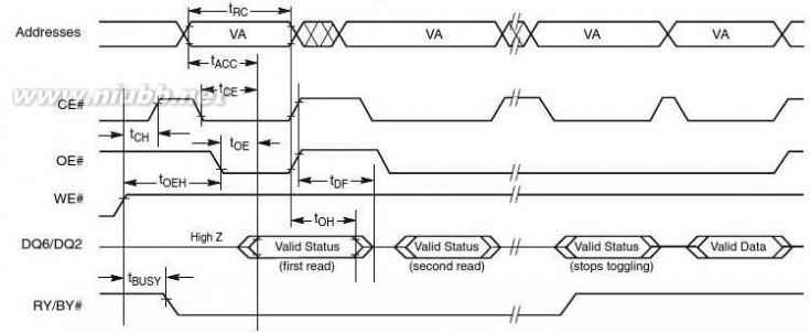
Figure 13.Data# Polling Timings (During Embedded Algorithms)
Note:VA = Valid address; not required for DQ6. Illustration shows first two status cycle after command sequence, last status read cycle, and array data read cycle.
Figure 14.Toggle Bit Timings (During Embedded Algorithms)
November1,200621503G5Am29F080B29
55se AM29F080B-55SE中文资料
元器件交易网www.cecb2b.com
DATA SHEET
AC CHARACTERISTICS
EnterEmbeddedErasing
扩展:at89c55中文资料 / tps40055中文资料 / 5562a中文资料
WE#
EraseEnter EraseSuspend Program
SuspendProgram
EraseResume
Erase Suspend
Read
Erase
Erase
Complete
Read
DQ6
DQ2
Note:The system may use OE# or CE# to toggle DQ2 and DQ6. DQ2 must be read at an address within the erase-suspended sector.
Figure 15.DQ2 vs. DQ6
Temporary Sector Unprotect
ParameterJEDEC
StdtVIDRtRSP
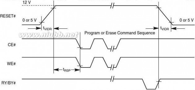
Note:Not 100% tested.
Description
VID Rise and Fall Time (See Note)RESET# Setup Time for Temporary Sector Unprotect
MinMin
All Speed Options
5004
Unitnsμs
Figure 16.Temporary Sector Group Unprotect Timing Diagram
30Am29F080B21503G5November1,2006
55se AM29F080B-55SE中文资料
元器件交易网www.cecb2b.com
DATA SHEET
AC CHARACTERISTICS
Erase and Program Operations
Alternate CE# Controlled Writes
Speed Options
Parameter Description
Write Cycle Time (Note 1)Address Setup TimeAddressHoldTimeDataSetupTimeData Hold Time
Read Recover Time Before Write CE# Setup TimeCE# Hold TimeWrite Pulse Width
Write Pulse Width High Byte Programming Operation (Note 2)Sector Erase Operation (Note 2)
MinMinMinMinMinMinMinMinMinMinTypTyp
30
35
2071
4525
4530
0000
45
50
-5555
-7070
-909004545
5050-120120
Unitnsnsnsnsnsnsnsnsnsnsμssec
Parameter SymboltAVAVtAVELtELAXtDVEHtEHDXtGHELtWLELtEHWHtELEHtEHELtWHWH1tWHWH2
tWCtAStAHtDStDHtGHELtWStWHtCPtCPHtWHWH1tWHWH2
Notes:
1.Not 100% tested.
2.See the “Erase And Programming Performance” section for more information.
November1,200621503G5Am29F080B31
55se AM29F080B-55SE中文资料
元器件交易网www.cecb2b.com
DATA SHEET
AC CHARACTERISTICS
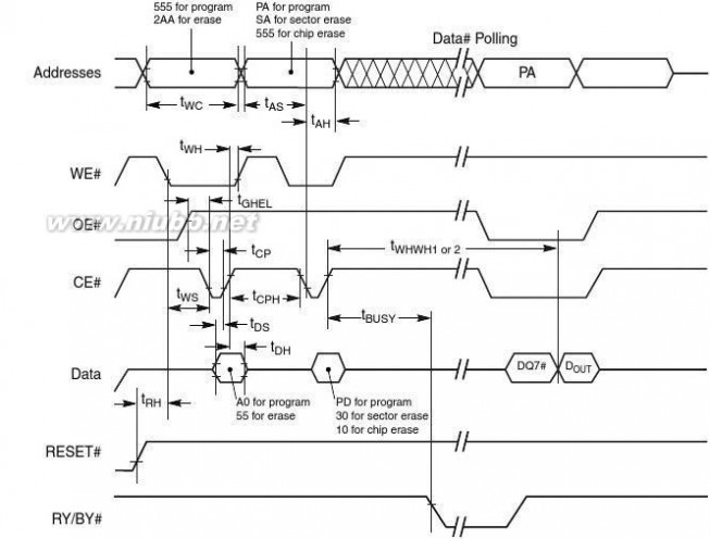
Notes:
1.PA = Program Address, PD = Program Data, SA = Sector Address, DQ7# = Complement of Data Input, DOUT = Array Data.
2.Figure indicates the last two bus cycles of the command sequence.
Figure 17.Alternate CE# Controlled Write Operation Timings
32Am29F080B21503G5November1,2006
55se AM29F080B-55SE中文资料
元器件交易网www.cecb2b.com
DATA SHEET
ERASE AND PROGRAMMING PERFORMANCE
Parameter
Sector Erase TimeChip Erase TimeByte Programming TimeChip Programming Time (Note 3)
Typ (Note 1)
1 1677.2
Max (Note 2)
812830021.6
Unitsecsecμssec
Comments
Excludes 00h programming prior to erasure (Note 4)
Excludes system-level overhead (Note 5)
Notes:
1.Typical program and erase times assume the following conditions: 25°C, 5.0 V VCC, 1,000,000 cycles. Additionally,
programming typicals assume checkerboard pattern.2.Under worst case conditions of 90°C, VCC = 4.5 V (4.75 for -55), 1,000,000 cycles.
3.The typical chip programming time is considerably less than the maximum chip programming time listed, since most bytes
program faster than the maximum byte program time listed. If the maximum byte program time given is exceeded, only then does the device set DQ5 = 1. See the section on DQ5 for further information.4.In the pre-programming step of the Embedded Erase algorithm, all bytes are programmed to 00h before erasure.
5.System-level overhead is the time required to execute the four-bus-cycle sequence for programming. See Table 4 for further
information on command definitions.6.The device has a typical erase and program cycle endurance of 1,000,000 cycles. 1,000,000 cycles are guaranteed.
LATCHUP CHARACTERISTIC
Min
Input Voltage with respect to VSS on I/O pinsVCC Current
Includes all pins except VCC. Test conditions: VCC = 5.0 Volt, one pin at a time.
–1.0 V–100 mA
MaxVCC + 1.0 V+100 mA
TSOP AND SO PIN CAPACITANCE
Parameter Symbol
CINCOUTCIN2
Parameter Description
Input CapacitanceOutput CapacitanceControl Pin Capacitance
VIN = 0VOUT = 0VIN = 0
Test Conditions
Min68.57.5
Max7.5129
UnitpFpFpF
Notes:
1.Sampled, not 100% tested.
2.Test conditions TA = 25°C, f = 1.0 MHz.
DATA RETENTION
Parameter
Minimum Pattern Data Retention Time
Test Conditions
150°C125°C
Min1020
UnitYearsYears
November1,200621503G5Am29F080B33
55se AM29F080B-55SE中文资料
元器件交易网www.cecb2b.com
DATA SHEET
PHYSICAL DIMENSIONS
SO 044—44-Pin Small Outline Package
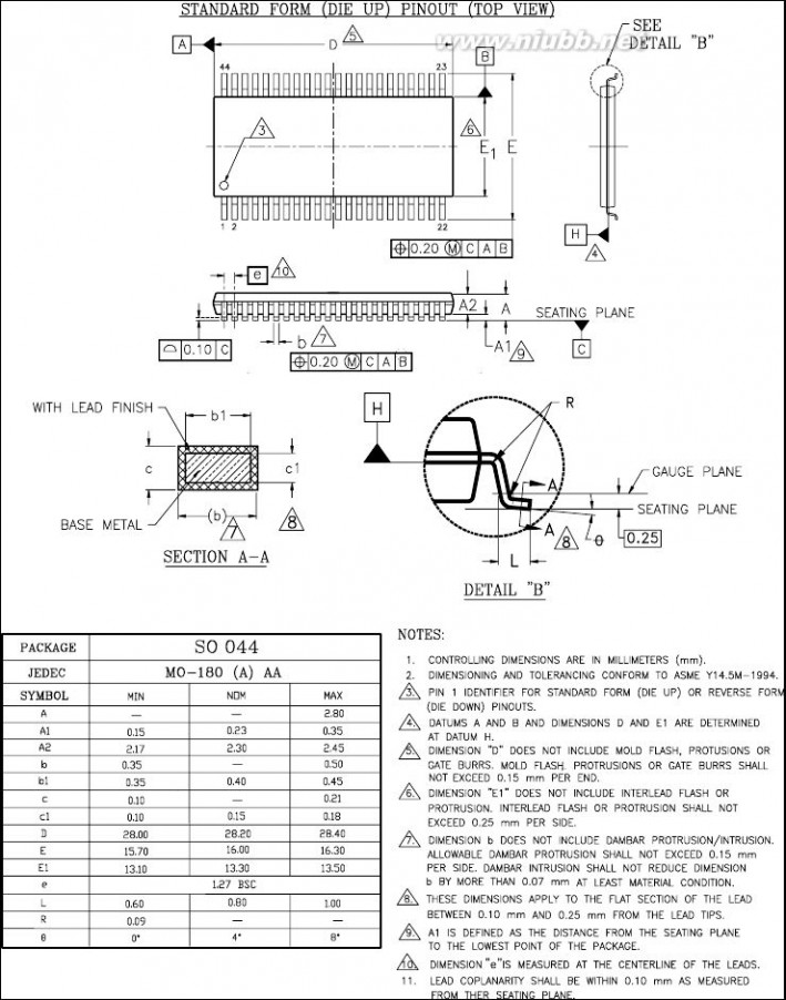
34Am29F080B21503G5November1,2006
55se AM29F080B-55SE中文资料 扩展:at89c55中文资料 / tps40055中文资料 / 5562a中文资料
元器件交易网www.cecb2b.com
DATA SHEET
PHYSICAL DIMENSIONS
TS 040—40-Pin Standard Thin Small Outline Package

November1,200621503G5Am29F080B35
55se AM29F080B-55SE中文资料
元器件交易网www.cecb2b.com
DATA SHEET
REVISION SUMMARY Revision A (July 1997)
Initial release.
Erase and Programming Performance
Changed minimum 100K program and erase cyclesguaranteed to 1,000,000.
Revision B (January 1998)
Global
Formatted for consistency with other 5.0 volt-onlydatasheets.
Figure 9, Read Operation Timings
Corrected RESET# waveform so that it is high for theduration of the read cycle.
Figure 11, Chip/Sector Erase Operation TimingsCorrected data unlock cycle in diagram to 55h.Figure 17, Alternate CE# Controlled Program Operation Timings
Corrected command for sector erase to 30h, chip eraseto 10h.
Revision E (January 1999)
Global
Updated for CS39S process technology.Distinctive CharacteristicsAdded:
■20-year data retention at 125°C
—Reliable operation for the life of the systemDC Characteristics—CMOS Compatible
Added note “For CMOS mode only, ICC3 = ICC4 = 20μAmax at extended temperatures (> +85°C)”.
DC Characteristics—TTL/NMOS Compatible and CMOS Compatible
ICC1, ICC2, ICC3, ICC4: Added Note 2 “Maximum ICCspecifications are tested with VCC = VCCmax”.ICC3, ICC4: Deleted VCC = VCCMax.
Revision C (January 1998)
Standby Mode
Removed sentence in first paragraph referring toRESET# pulse.
Sector Group Protection/Unprotection, Temporary Sector Group Unprotect
Changed references from “sector” to “sector group”.Corrected text to indicate sector groups are composedof two adjacent sectors.
Revision E+1 (March 23, 1999)
Operating Ranges
The temperature ranges are now specified as ambient.
Revision E+2 (April 9, 1999)
Ordering Information, Operating RangesAdded the extended temperature range.
Revision D (May 1998)
Distinctive Characteristics
Changed minimum 100K write/erase cycles guaran-teed to 1,000,000.
DC Characteristics, CMOS Compatible
For ICC3 and ICC4, the voltage tolerances given for CE#and RESET# are now ±0.5 V.AC Characteristics
Erase/Program Operations; Erase and Program Oper-ations Alternate CE# Controlled Writes: Corrected thenotes reference for tWHWH1 and tWHWH2. These param-eters are 100% tested. Corrected the note reference fortVCS. This parameter is not 100% tested.Temporary Sector Unprotect Table
Added note reference for tVIDR. This parameter is not100% tested.
Command Definitions
Corrected the shift in the table header.
Revision F (November 15, 1999)
AC Characteristics—Figure 11. Program
Operations Timing and Figure 12. Chip/Sector Erase Operations
Deleted tGHWL and changed OE# waveform to start athigh.
Physical Dimensions
Replaced figures with more detailed illustrations.
Revision F+1 (May 18, 2000)
DC Characteristics
TTL/NMOS Compatible: The ICC2 specifications arenow identical to those for CMOS compatible.
Revision G (December 4, 2000)
Added table of contents.Ordering InformationDeleted burn-in option.
36Am29F080B21503G5November1,2006
55se AM29F080B-55SE中文资料
元器件交易网www.cecb2b.com
DATA SHEET
Revision G+1 (January 3, 2002)
Global
Changed -75 speed option to -70 (70 ns, VCC = 5.0 ±
10 %). Added -55 (55 ns, VCC = 5.0 V ± 5%) speed
option.Revision G3 (December 22, 2005)GlobalDeleted 150 ns speed option and reverse TSOP pack-age option.
Revision G+2 (June 14, 2004)
Ordering Information
Added Pb-free OPNs.Revision G4 (May 19, 2006)Added “Not recommended for new designs” note.AC CharacteristicsChanged tBUSY specification to maximium value.
Revision G5 (November 1, 2006)
Deleted “Not recommended for new designs” note.
Colophon
The products described in this document are designed, developed and manufactured as contemplated for general use, including without limita-tion, ordinary industrial use, general office use, personal use, and household use, but are not designed, developed and manufactured as con-templated (1) for any use that includes fatal risks or dangers that, unless extremely high safety is secured, could have a serious effect to the public, and could lead directly to death, personal injury, severe physical damage or other loss (i.e., nuclear reaction control in nuclear facility, aircraft flight control, air traffic control, mass transport control, medical life support system, missile launch control in weapon system), or (2) for any use where chance of failure is intolerable (i.e., submersible repeater and artificial satellite). Please note that Spansion Inc. will not be liable to you and/or any third party for any claims or damages arising in connection with above-mentioned uses of the products. Any semiconductor devices have an inherent chance of failure. You must protect against injury, damage or loss from such failures by incorporating safety design measures into your facility and equipment such as redundancy, fire protection, and prevention of over-current levels and other abnormal operating conditions. If any products described in this document represent goods or technologies subject to certain restrictions on export under the Foreign Exchange and Foreign Trade Law of Japan, the US Export Administration Regulations or the applicable laws of any other country, the prior au-thorization by the respective government entity will be required for export of those products.
扩展:at89c55中文资料 / tps40055中文资料 / 5562a中文资料
Trademarks
Copyright ? 2006 Spansion Inc. All Rights Reserved. Spansion, the Spansion logo, MirrorBit, ORNAND, HD-SIM, and combinations thereof are trademarks of Spansion Inc. Other names are for informational purposes only and may be trademarks of their respective owners.
Copyright ? 2004–2006 Advanced Micro Devices, Inc. All rights reserved. AMD, the AMD logo, ExpressFlash, and combinations thereof are trademarks of Advanced Micro Devices, Inc. Product names used in this publication are for identification purposes only and may be trademarks of their respective companies.
November1,200621503G5Am29F080B37
扩展:at89c55中文资料 / tps40055中文资料 / 5562a中文资料
本文标题:中文资料-WT2220ML450A中文资料61阅读| 精彩专题| 最新文章| 热门文章| 苏ICP备13036349号-1