一 : AD7998BRUZ-0REEL3中文资料
元器件交易网www.61k.com
8-Channel, 10- and 12-Bit ADCs with I2C-Compatible Interface in 20-Lead TSSOP
FEATURES
10- and 12-bit ADC with fast conversion time: 2 μs typ 8 single-ended analog input channels Specified for VDD of 2.7 V to 5.5 V Low power consumption
Fast throughput rate: up to 188 kSPS Sequencer operation Automatic cycle mode
I2C?-compatible serial interface supports standard, fast, and high speed modes
Out-of-range indicator/alert function Pin-selectable addressing via AS Shutdown mode: 1 μA max
Temperature range: ?40°C to +85°C 20-lead TSSOP package
See the AD7992 and AD7994 for 2-channel and 4-channel equivalent devices, respectively
GENERAL DESCRIPTION
The AD7997/AD7998 are 8-channel, 10- and 12-bit, low power, successive approximation ADCs with an I2C-compatible
interface. The parts operate from a single 2.7 V to 5.5 V power supply and feature a 2 μs conversion time. The parts contain an 8-channel multiplexer and track-and-hold amplifier that can handle input frequencies up to 11 MHz.
The AD7997/AD7998 provide a 2-wire serial interface that is compatible with I2C interfaces. Each part comes in two versions, AD7997-0/AD7998-0 and AD7997-1/AD7998-1, and each version allows at least two different I2C addresses. The I2C interface on the AD7997-0/AD7998-0 supports standard and fast I2C interface modes. The I2C interface on the AD7997-1/ AD7998-1 supports standard, fast, and high speed I2C interface modes.
The AD7997/AD7998 normally remain in a shutdown state while not converting, and power up only for conversions. The conversion process can be controlled using the CONVSTby a command mode where conversions occur across I2C write operations or an automatic conversion interval mode selected through software control.
The AD7997/AD7998 require an external reference that should be applied to the REFIN pin and can be in the range of 1.2 V to VDD. This allows the widest dynamic input range to the ADC.
Rev. 0
Information furnished by Analog Devices is believed to be accurate and reliable. However, no responsibility is assumed by Analog Devices for its use, nor for any infringements of patents or other rights of third parties that may result from its use. Specifications subject to change without notice. No license is granted by implication or otherwise under any patent or patent rights of Analog Devices. Trademarks and registered trademarks are the property of their respective owners.
AD7997/AD7998
FUNCTIONAL BLOCK DIAGRAM
VIN
VIN1
00-0-37430Figure 1.
On-chip limit registers can be programmed with high and low limits for the conversion result, and an open-drain, out-of-range indicator output (ALERT) becomes active when the programmed high or low limits are violated by the conversion result. This output can be used as an interrupt.
PRODUCT HIGHLIGHTS
1. 2 μs conversion time with low power consumption. 2. I2C-compatible serial interface with pin-selectable
addresses. Two AD7997/AD7998 versions allow five AD7997/AD7998 devices to be connected to the same serial bus. 3. The parts feature automatic shutdown while not converting
to maximize power efficiency. Current consumption is 1 μA max when in shutdown mode at 3V. 4. Reference can be driven up to the power supply. 5. Out-of-range indicator that can be software disabled or
enabled. 6. One-shot and automatic conversion rates.
7. Registers store minimum and maximum conversion
results.
One Technology Way, P.O. Box 9106, Norwood, MA 02062-9106, U.S.A. Tel: 781.329.4700 www.61k.comFax: 781.326.8703? 2004 Analog Devices, Inc. All rights reserved.
元器件交易网www.61k.com
AD7997/AD7998
TABLE OF CONTENTS
AD7997 Specifications.....................................................................3 AD7998 Specifications.....................................................................5 I2C Timing Specifications................................................................7 Absolute Maximum Ratings............................................................9 ESD Caution..................................................................................9 Pin Configuration and Pin Function Descriptions....................10 Terminology....................................................................................11 Typical Performance Characteristics...........................................12 Circuit Information........................................................................15 Converter Operation..................................................................15 Typical Connection Diagram...................................................16 Analog Input...............................................................................16 Internal Register Structure............................................................18 Address Pointer Register...........................................................18 Configuration Register..............................................................19 Conversion Result Register.......................................................20 Limit Registers............................................................................20 Alert Status Register (CH1 to CH4)........................................21 Cycle Timer Register..................................................................22 Sample Delay and Bit Trial Delay.............................................22 Serial Interface................................................................................23
Serial Bus Address......................................................................23 Writing to the AD7997/AD7998..................................................24 Writing to the Address Pointer Register for a Subsequent
Read..............................................................................................24 Writing a Single Byte of Data to the Alert Status Register or Cycle Register..............................................................................24 Writing Two Bytes of Data to a Limit, Hysteresis, or
Configuration Register..............................................................24 Reading Data from the AD7997/AD7998...................................26 ALERT/BUSY Pin..........................................................................27 SMBus ALERT............................................................................27 BUSY............................................................................................27 Placing the AD7997-1/AD7998-1 into High Speed Mode...27 The Address Select (AS) Pin.....................................................27 Modes of Operation.......................................................................28 Mode 1—Using the CONVST Pin...........................................28 Mode 2 – COMMAND MODE...............................................29 Mode 3—Automatic Cycle Interval Mode..............................30 Outline Dimensions.......................................................................31 Ordering Guide..........................................................................31 Related Parts in I2C-Compatible ADC Product Family........31
REVISION HISTORY
9/04—Revision 0: Initial Version
Rev. 0 | Page 2 of 32
元器件交易网www.61k.com
AD7997/AD7998
AD7997 SPECIFICATIONS
Temperature range for B version is ?40°C to +85°C. Unless otherwise noted, VDD = 2.7 V to 5.5 V; REFIN = 2.5 V; For the AD7997-0, all specifications apply for fSCL up to 400 kHz; for the AD7997-1, all specifications apply for fSCL up to 3.4 MHz, unless otherwise noted; TA = TMIN to TMAX.
Rev. 0 | Page 3 of 32
元器件交易网www.61k.com
AD7997/AD7998

Max/min ac dynamic performance, INL and DNL specifications are typical specifications when operating in Mode 2 with I2C Hs-Mode SCL frequencies. Specifications outlined for Mode 2 apply to Mode 3 also. Sample delay and bit trial delay enabled.
2 See the Terminology section.
3 Guaranteed by initial characterization.
1
Rev. 0 | Page 4 of 32
元器件交易网www.61k.com
AD7997/AD7998
AD7998 SPECIFICATIONS
Temperature range for B version is ?40°C to +85°C. Unless otherwise noted, VDD = 2.7 V to 5.5 V; REFIN = 2.5 V; For the AD7998-0, all specifications apply for fSCL up to 400 kHz; for the AD7998-1, all specifications apply for fSCL up to 3.4 MHz, unless otherwise noted; TA = TMIN to TMAX.
Rev. 0 | Page 5 of 32
元器件交易网www.61k.com
AD7997/AD7998

Max/min ac dynamic performance, INL and DNL specifications are typical specifications when operating in Mode 2 with I2C Hs-Mode SCL frequencies. Specifications outlined for Mode 2 apply to Mode 3 also. Sample delay and bit trial delay enabled.
2 See the Terminology section.
3 Guaranteed by initial characterization.
1
Rev. 0 | Page 6 of 32
元器件交易网www.61k.com
AD7997/AD7998
I2C TIMING SPECIFICATIONS
Guaranteed by initial characterization. All values measured with input filtering enabled. CB refers to capacitive load on the bus line. tr and tf measured between 0.3 VDD and 0.7 VDD.
High speed mode timing specifications apply to the AD7997-1/AD7998-1 only. Standard and fast mode timing specifications apply to both the AD7997-0/AD7998-0 and the AD7997-1/AD7998-1. See Figure 2. Unless otherwise noted, VDD = 2.7 V to 5.5 V; REFIN = 2.5 V; TA =TMIN to TMAX. Table 3.
AD7997/AD7998 Limit at TMIN, TMAXin ax Unit fSCL Standard mode 100 kHz Fast mode 400 kHz High speed mode CB = 100 pF max 3.4 MHz CB = 400 pF max 1.7 MHz t1 Standard mode 4 μs Fast mode 0.6 μs High speed mode CB = 100 pF max 60 ns CB = 400 pF max 120 ns t2 Standard mode 4.7 μs Fast mode 1.3 μs High speed mode CB = 100 pF max 160 ns CB = 400 pF max ns 320 t3 Standard mode 250 ns Fast mode 100 ns High speed mode 10 ns t41Standard mode 0 3.45 μs Fast mode 0 0.9 μs High speed mode CB = 100 pF max 0 702ns CB = 400 pF max 0 150 ns t5 Standard mode 4.7 μs Fast mode 0.6 μs High speed mode 160 ns t6 Standard mode 4 μs μs High speed mode 160 ns t7 Standard mode 4.7 μs μs t8 Standard mode 4 μs Fast mode 0.6 μs High speed mode 160 ns t9 Standard mode 1000 ns Fast mode 20 + 0.1 CB 300 ns High speed mode CB = 100 pF max 10 80 ns CB = 400 pF max 20 160 ns
Description
Serial clock frequency
tHIGH, SCL high time
tLOW, SCL low time
tSU;DAT, data setup time
tHD;DAT, data hold time
tSU;STA, setup time for a repeated start condition
tHD;STA, hold time (repeated) start condition
tBUF, bus free time between a stop and a start condition
tSU;STO, setup time for stop condition
tRDA, rise time of SDA signal
Rev. 0 | Page 7 of 32
元器件交易网www.61k.com
AD7997/AD7998
t10Standard mode Fast mode High speed mode CB = 100 pF max CB = 400 pF max t11 Standard mode Fast mode High speed mode CB = 100 pF max CB = 400 pF max t11AStandard mode t12 tSP
tPOWER-UP
Fast mode
High speed mode CB = 100 pF max CB = 400 pF max Standard mode Fast mode
High speed mode CB = 100 pF max CB = 400 pF max Fast mode
High speed mode
AD7997/AD7998 Limit at TMIN, TMAXin ax Unit 300 ns 20 + 0.1 CB300 ns 10 80 ns 20 160 ns 1000 ns 20 + 0.1 CB300 ns

10 40 ns 20 80 ns 1000 ns 20 + 0.1 CB 10 20
20 + 0.1 CB 10 20 0 0 1
300 80 160 300 300 40 80 50 10
ns ns ns ns ns ns ns ns ns typ μs
Description
tFDA, fall time of SDA signal
tRCL, rise time of SCL signal
tRCL1, rise time of SCL signal after a repeated start condition and after an Acknowledge bit
tFCL, fall time of SCL signal
Pulse width of suppressed spike
Power-up time
12
A device must provide a data hold time for SDA in order to bridge the undefined region of the SCL falling edge. For 3 V supplies, the maximum hold time with CB = 100 pF max is 100 ns max.
MM
03473-0-002
S = START CONDITIONP = STOP CONDITION
Figure 2. Timing Diagram for 2-Wire Serial Interface
Rev. 0 | Page 8 of 32
元器件交易网www.61k.com
AD7997/AD7998
Stresses above those listed under Absolute Maximum Ratings ABSOLUTE MAXIMUM RATINGS TA = 25°C, unless otherwise noted. Table 4. may cause permanent damage to the device. This is a stress VDD to GND ?0.3 V to 7 V rating only; functional operation of the device at these or any Analog Input Voltage to GND ?0.3 V to VDD + 0.3 V other conditions above those listed in the operational sections Reference Input Voltage to GND ?0.3 V to VDD + 0.3 V of this specification is not implied. Exposure to absolute Digital Input Voltage to GND ?0.3 V to +7 V maximum rating conditions for extended periods may affect Digital Output Voltage to GND ?0.3 V to VDD + 0.3 V device reliability. Input Current to Any Pin Except Supplies1±10 mA
Operating Temperature Range
Commercial (B Version) ?40°C to +85°C
Storage Temperature Range ?65°C to +150°
Junction Temperature 150°C
20-Lead TSSOP
θJA Thermal Impedance 143°C/W
θJC Thermal Impedance 45°C/W
Pb/SN Temperature, Soldering
Reflow (10 s to 30 s) 240 (+0/-5)°C
Pb-free Temperature, Soldering
(+0)°C
kV
1 Transient currents of up to 100 mA do not cause SCR latch-up.

ESD CAUTION
ESD (electrostatic discharge) sensitive device. Electrostatic charges as high as 4000 V readily accumulate on the human body and test equipment and can discharge without detection. Although this product features proprietary ESD protection circuitry, permanent damage may occur on devices subjected to high energy electrostatic discharges. Therefore, proper ESD precautions are recommended to avoid performance degradation or loss of functionality.
Rev. 0 | Page 9 of 32
元器件交易网www.61k.com
AD7997/AD7998
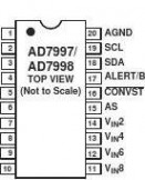
AGNDVDDAGNDAGNDVDDREFINVIN1VIN3VIN5
03473-0-003
Figure 3. AD7998/AD7997 Pin Configuration
VIN7Table 6. I2C Address Selection
Part Number AD7997-0 AD7997-0 AD7997-1 AD7997-1 AD7997-x1AD7998-0 AD7998-0 AD7998-1 AD7998-1 AD7998-x1
AS Pin I2C Address AGND 010 0001 VDD 010 0010 AGND 010 0011 VDD 010 0100 Float 010 0000 AGND 010 0001 VDD 010 0010 AGND 010 0011 VDD 010 0100
0000
1
If the AS pin is left floating on any of the AD7997/AD7998 parts, the device address is 010 0000.
Rev. 0 | Page 10 of 32
元器件交易网www.61k.com
AD7997/AD7998
Channel-to-Channel Isolation
A measure of the level of crosstalk between channels, taken by applying a full-scale sine wave signal to the unselected input channels, and determining how much the 108 Hz signal is
attenuated in the selected channel. The sine wave signal applied to the unselected channels is then varied from 1 kHz up to 2 MHz, each time determining how much the 108 Hz signal in the selected channel is attenuated. This figure represents the worst-case level across all channels.
Aperture Delay
The measured interval between the sampling clock’s leading edge and the point at which the ADC takes the sample. Aperture Jitter
This is the sample-to-sample variation in the effective point in time at which the sample is taken.
Full-Power Bandwidth
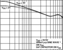
The input frequency at which the amplitude of the reconstructed fundamental is reduced by 0.1 dB or 3 dB for a full-scale input. Power Supply Rejection Ratio (PSRR)
The ratio of the power in the ADC output at the full-scale frequency, f, to the power of a 200 mV p-p sine wave applied to the ADC VDD supply of frequency fS: PSRR (dB) = 10 log (Pf/PfS)
where Pf is the power at frequency f in the ADC output; PfS is the power at frequency fS coupled onto the ADC VDD supply. Integral Nonlinearity
The maximum deviation from a straight line passing through the endpoints of the ADC transfer function. The endpoints are zero scale, a point 1 LSB below the first code transition, and full scale, a point 1 LSB above the last code transition. Differential Nonlinearity
The difference between the measured and the ideal 1 LSB change between any two adjacent codes in the ADC. Offset Error
The deviation of the first code transition (00…000) to (00…001) from the ideal—that is, AGND + 1 LSB. Offset Error Match
The difference in offset error between any two channels. Gain Error
The deviation of the last code transition (111…110) to (111…111) from the ideal (that is, REFIN ? 1 LSB) after the offset error has been adjusted out.
Gain Error Match
The difference in gain error between any two channels.
TERMINOLOGY
Signal-to-Noise and Distortion Ratio (SINAD)
The measured ratio of signal-to-noise and distortion at the out-put of the A/D converter. The signal is the rms amplitude of the fundamental. Noise is the sum of all nonfundamental signals up to half the sampling frequency (fS/2), excluding dc. The ratio is dependent on the number of quantization levels in the digiti-zation process; the more levels, the smaller the quantization noise. The theoretical signal-to-noise and distortion ratio for an ideal N-bit converter with a sine wave input is given by Signal-to-(Noise + Distortion) = (6.02 N + 1.76) dB Thus, the SINAD is 61.96 dB for a 10-bit converter and 74 dB for a 12-bit converter.
Total Harmonic Distortion (THD)
The ratio of the rms sum of harmonics to the fundamental. For the AD7997/AD7998, it is defined as
V22+V32+V42+V52+V62
THD(dB)=20log
V1
where V1 is the rms amplitude of the fundamental and V2, V3, V4, V5, and V6 are the rms amplitudes of the second through sixth harmonics.
Peak Harmonic or Spurious Noise
The ratio of the rms value of the next largest component in the ADC output spectrum (up to fS/2 and excluding dc) to the rms value of the fundamental. Typically, the value of this specification is determined by the largest harmonic in the spectrum, but for ADCs where the harmonics are buried in the noise floor, it is a noise peak.
Intermodulation Distortion
With inputs consisting of sine waves at two frequencies, fa and fb, any active device with nonlinearities creates distortion products at sum and difference frequencies of mfa ± nfb, where m, n = 0, 1, 2, 3, and so on. Intermodulation distortion terms are those for which neither m nor n equal zero. For example, second-order terms include (fa + fb) and (fa ? fb), while third-order terms include (2fa + fb), (2fa ? fb),(fa + 2fb) and (fa ? 2fb).
The AD7997/AD7998 is tested using the CCIF standard where two input frequencies near the top end of the input bandwidth are used. In this case, the second-order terms are usually dis-tanced in frequency from the original sine waves while the third-order terms are usually at a frequency close to the input frequencies. As a result, the second and third-order terms are specified separately. The calculation of intermodulation distor-tion is, like the THD specification, the ratio of the rms sum of the individual distortion products to the rms amplitude of the sum of the fundamentals, expressed in dB.
Rev. 0 | Page 11 of 32
元器件交易网www.61k.com
AD7997/AD7998
TYPICAL PERFORMANCE CHARACTERISTICS
0–20
–40
)
Bd( DA–60
NIS–80
–100
–120
020
4060FREQUENCY (kHz)
Figure 4. AD7998 Dynamic Performance with 5 V Supply and
2.5 V Reference, 121 kSPS, Mode 1
–10
–30
)
Bd( –50
DANIS–70
–90–110
INPUT FREQUENCY (kHz)
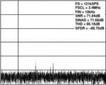
Figure 5. AD7997 Dynamic Performance with 5 V Supply and
2.5 V Reference, 121 kSPS, Mode 1
100
9080)
70Bd( RR60SP50403020SUPPLY RIPPLE FREQUENCY(kHz)
Figure 6. PSRR vs. Supply Ripple Frequency
757065
)
Bd60(
DANIS55
50
454
40
0-0-37430
FREQUENCY(kHz)
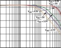
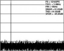
Figure 7. AD7998 SINAD vs. Analog Input Frequency for
Various Supply Voltages, 3.4 MHz fSCL, 136 kSPS
1.00.80.60.4
)
BLS0.2( ROR0R EL–0.2NI–0.4
–0.6–0.8
5
00–1.0
-0-305001000150020002500300035004000
7430
CODE
Figure 8. Typical INL, VDD = 5.5 V, Mode 1, 3.4 MHz fSCL, 121 kSPS
1.00.80.6
)
0.4BLS(0.2 ROR0R EL–0.2ND–0.4–0.6–0.8
6
0–1.0
0-0-0
500
1000
1500
20002500
3000
3500
4000
37430
CODE
Figure 9. Typical DNL, VDD = 5.5 V, Mode 1, 3.4 MHz fSCL, 121 kSPS
Rev. 0 | Page 12 of 32
700-0-374308
00-0-374309
00-0-37430
元器件交易网www.61k.com
1.00.80.6
AD7997/AD7998
1.00.80.6DNL ERROR (LSB)
0.40.40.20–0.2–0.4-0.6–0.8
INL ERROR (LSB)
0.20–0.2–0.4–0.6–0.8
500
1000
1500
2000CODE
2500
3000
3500
4000
03473-0-01
1.72.2
2.73.23.74.24.7
REFERENCE VOLTAGE (V)
03473-0-013
–1.0
–1.0
1.2
Figure 10. Typical INL, VDD = 2.7 V, Mode 1, 3.4 MHz fSCL, 121 kSPS
1.00.80.6
Figure 13. AD7998 Change in DNL vs. Reference Voltage VDD = 5 V,
Mode 1, 121 kSPS
0.00070.0006
SUPPLY CURRENT (mA)
DNL ERROR (LSB)
0.40.20–0.2–0.4–0.6
0.0005
–40°C
0.00040.0003
°C
0.00020.0001
+25°C
–0.8
03473-0-01
1
0500100015002000CODE
2500300035004000
3.23.74.24.75.2
SUPPLY VOLTAGE (V)
03473-0-01403473-0-015
–1.0
02.7
Figure 11. Typical DNL, VDD = 2.7 V, Mode 1, 3.4 MHz fSCL, 121 kSPS
1.0

0.80.6
2.01.81.6
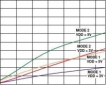
Figure 14. AD7998 Shutdown Current vs. Supply Voltage,
–40°C, +25°C, and +85°C
SUPPLY CURRENT (mA)
0.4INL ERROR (LSB)
1.41.21.00.80.60.40.2
0.20–0.2–0.4-0.6–0.8
1.7
2.2
2.7
3.2
3.7
4.2
4.7
03473-0-012
–1.0
1.20REFERENCE VOLTAGE (V)
SCL FREQUENCY (kHz)
Figure 12. AD7998 Change in INL vs. Reference Voltage VDD = 5 V,
Mode 1, 121 kSPS Figure 15. AD7998 Average Supply Current vs. I2C Bus Rate for
VDD = 3 V and 5 V
Rev. 0 | Page 13 of 32
元器件交易网www.61k.com
AD7997/AD7998
2.01.81.6
12.0
11.811.611.411.2
727374
Y CURRENT (mA)
1.41.21.0
NOB (BITS)
71

0.8SINAD (dB)
LPUPS0.60.40.2
02.7
3.23.74.24.75.2
SUPPLY VOLTAGE (V)
Figure 16. AD7998 Average Supply Current vs. Supply Voltage
for Various Temperatures
E11.070
10.8
69
10.66
110.4
68
0-01.2002.0482.5002.7003.0003.3004.0964.5005.000
-37430
REFERENCE VOLTAGE (V)
Figure 17. SINAD/ENOB vs. Reference Voltage, Mode 1, 121 kSPS
Rev. 0 | Page 14 of 32
7
10-0-37430
元器件交易网www.61k.com
AD7997/AD7998
At the beginning of a conversion, SW2 opens and SW1 moves to position B, causing the comparator to become unbalanced, as shown in Figure 19. The input is disconnected once the con-version begins. The control logic and the capacitive DAC are used to add and subtract fixed amounts of charge from the sampling capacitor to bring the comparator back into a
balanced condition. When the comparator is rebalanced, the conversion is complete. The control logic generates the ADC
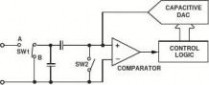
output code. Figure 20 shows the ADC transfer characteristic.
CIRCUIT INFORMATION
The AD7997/AD7998 are low power, 10- and 12-bit, single-supply, 8-channel A/D converters. The parts can be operated from a 2.7 V to 5.5 V supply.
The AD7997/AD7998 have an 8-channel multiplexer, an on-chip track-and-hold, an A/D converter, an on-chip oscillator, internal data registers, and an I2C-compatible serial interface, all housed in a 20-lead TSSOP. This package offers considerable space-saving advantages over alternative solutions. The
AD7997/AD7998 require an external reference in the range of 1.2 V to VDD.
The AD7997/AD7998 typically remain in a power-down state while not converting. When supplies are first applied, the parts come up in a power-down state. Power-up is initiated prior to a conversion, and the device returns to shutdown when the conversion is complete. Conversions can be initiated on the CONVSTautomatic cycle interval mode, or a command mode where wake-up and a conversion occur during a write address function (see the Modes of Operation section). When the conversion is complete, the AD7997/AD7998 again enter
shutdown mode. This automatic shutdown feature allows power saving between conversions. This means any read or write operation across the I2C interface can occur while the device is in shutdown.
VIN
AGND
03473-0-019
Figure 19. ADC Conversion Phase
ADC Transfer Function
The output coding of the AD7997/AD7998 is straight binary. The designed code transitions occur at successive integer LSB values (1 LSB, 2 LSB, and so on). The LSB size is REFIN/1024 for the AD7997 and REFIN/4096 for the AD7998. Figure 20 shows
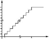
the ideal transfer characteristic for the AD7997/AD7998.
111...111111...110
CONVERTER OPERATION
The AD7997/AD7998 are successive approximation analog-to-digital converters based around a capacitive DAC. Figure 18 and Figure 19 show simplified schematics of the ADC during the acquisition and conversion phase, respectively. Figure 18 shows the acquisition phase. SW2 is closed and SW1 is in position A, the comparator is held in a balanced condition, and the sampling capacitor acquires the signal on VIN.
ADCCODE
111...000011...111000...010000...001000...000
ANALOGINPUT0V TO REFIN
03473-0-020
Figure 20. AD7997/AD7998 Transfer Characteristic
VIN
0347AGND
Figure 18. ADC Acquisition Phase
Rev. 0 | Page 15 of 32
元器件交易网www.61k.com
AD7997/AD7998
TYPICAL CONNECTION DIAGRAM
The typical connection diagram for the AD7997/AD7998 is shown in Figure 22. In this figure, the address select pin (AS) is tied to VDD; however, AS can also be tied to AGND or left floating, allowing the user to select up to five AD7997/AD7998 devices on the same serial bus. An external reference must be applied to the AD7997/AD7998. This reference can be in the range of 1.2 V to VDD. A precision reference like the REF 19x family, AD780, ADR03, or ADR381 can be used to supply the reference voltage to the ADC.
SDA and SCL form the 2-wire I2C-/SMBus-compatible
interface. External pull-up resisters are required for both SDA and SCL lines.
The AD7998-0/AD7997-0 support standard and fast I2C
interface modes. The AD7998-1/AD7997-1 support standard, fast, and high speed I2C interface modes. Therefore if operating in either standard or fast mode, up to five AD7997/AD7998 devices can be connected to the bus, as noted:
3 × AD7997-0/AD7998-0 and 2 × AD7997-1/ AD7998-1 or
3 × AD7997-1/AD7998-1 and 2 × AD7997-0/AD7998-0 In high speed mode, up to three AD7997-1/AD7998-1 devices can be connected to the bus.
Wake-up from shutdown and acquisition prior to a conversion is approximately 1 μs, and conversion time is approximately 2 μs. The AD7997/AD7998 enters shutdown mode again after each conversion, which is useful in applications where power consumption is a concern.
ANALOG INPUT
Figure 21 shows an equivalent circuit of the AD7997/AD7998 analog input structure. The two diodes, D1 and D2, provide ESD protection for the analog inputs. Care must be taken to ensure that the analog input signal does not exceed the supply rails by more than 300 mV. This causes the diodes to become forward biased and start conducting current into the substrate. These diodes can conduct a maximum current of 10 mA without causing irreversible damage to the part.
VIN
03473-0-022
Figure 21. Equivalent Analog Input Circuit
Capacitor C1 in Figure 21 is typically about 4 pF and can primarily be attributed to pin capacitance. Resistor R1 is a lumped component made up of the on resistance (RON) of a track-and-hold switch, and also includes the RON of the
input multiplexer. The total resistance is typically about 400 ?. C2, the ADC sampling capacitor, has a typical capacitance of 30 pF.
03473-0-021
Rev. 0 | Page 16 of 32
元器件交易网www.61k.com
AD7997/AD7998
For ac applications, removing high frequency components from –40
the analog input signal is recommended, by using an RC band-
pass filter on the relevant analog input pin. In applications where –50
harmonic distortion and signal-to-noise ratio are critical, the analog input should be driven from a low impedance source. –60)
Large source impedances significantly affect the ac performance Bd(
of the ADC. This may necessitate the use of an input buffer D–70
HT
amplifier. The choice of the op amp is a function of the particular application. –80When no amplifier is used to drive the analog input, the source –90impedance should be limited to low values. The maximum source
impedance depends on the amount of total harmonic distortion –100(THD) that can be tolerated. THD increases as the source imped-INPUT FREQUENCY(kHz)
ance increases, and performance degrades. Figure 23 shows the
THD vs. the analog input signal frequency when using supply Figure 23. THD vs. Analog Input Frequency for Various voltages of 3 V ± 10% and 5 V ± 10%. Figure 24 shows the THD Supply Voltages, FS = 136 kSPS, Mode 1
vs. the analog input signal frequency for different source –40impedances.
–50–60
)

Bd( D–70
HT–80
–90–100INPUT FREQUENCY(kHz)
Figure 24. THD vs. Analog Input Frequency for Various
Source Impedances for VDD = 5 V, 136 kSPS, Mode 1
Rev. 0 | Page 17 of 32 320-0-37430 420-0-37430
元器件交易网www.61k.com
AD7997/AD7998
INTERNAL REGISTER STRUCTURE
The AD7997/AD7998 contain 17 internal registers that are used to store conversion results, high and low conversion limits, and information to configure and control the device (see Figure 25). Sixteen are data registers and one is an address pointer register. Each data register has an address that the address pointer register points to when communicating with it. The conversion result register is the only data register that is read only.
03473-0-025
ADDRESS POINTER REGISTER
Because it is the register to which the first data byte of every write operation is written automatically, the address pointer register does not have and does not require an address. The address pointer register is an 8-bit register in which the 4 LSBs are used as pointer bits to store an address that points to one of the AD7997/AD7998’s data registers. The 4 MSBs are used as command bits when operating in Mode 2 (see the Modes of Operation section). The first byte following each write address is to the address pointer register, containing the address of one of the data registers. The 4 LSBs select the data register to which subsequent data bytes are written. Only the 4 LSBs of this register are used to select a data register. On power-up, the address
pointer register contains all 0s, pointing to the conversion result register.
Table 7. Address Pointer Register
Register Select
Table 8. AD7997/AD7998 Register Addresses
0 0 0 0 Conversion Result Register (Read) 0 0 0 1 Alert Status Register (Read/Write) 0 0 1 0 Configuration Register (Read/Write) 0 0 1 1 Cycle Timer Register (Read/Write) 0 1 0 0 DATALOW Reg CH1 (Read/Write) 0 1 0 1 DATAHIGH Reg CH1 (Read/Write) 0 1 1 0 Hysteresis Reg CH1 (Read/Write) 0 1 1 1 DATALOW Reg CH2 (Read/Write) 1 0 0 0 DATAHIGH Reg CH2 (Read/Write) 1 0 0 1 Hysteresis Reg CH2 (Read/Write) 1 0 1 0 DATALOW Reg CH3 (Read/Write) 1 0 1 1 DATAHIGH Reg CH3 (Read/Write) 1 1 0 0 Hysteresis Reg CH3 (Read/Write) 1 1 0 1 DATALOW Reg CH4 (Read/Write) 1 1 1 0 DATAHIGH Reg CH4 (Read/Write) Reg CH4
(Read/Write)
Figure 25. AD7997/AD7998 Register Structure
Rev. 0 | Page 18 of 32
元器件交易网www.61k.com
AD7997/AD7998
CONFIGURATION REGISTER
The configuration register is a 16-bit read/write register that is used to set the operating mode of the AD7997/AD7998. The 4 MSBs of the register are unused. The bit functions of all 12 LSBs of the configuration register are outlined in Table 9. A 2-byte write is necessary when writing to the configuration register. Table 9. Configuration Register Bits and Default Settings at Power-Up
D15 D2
ALERT
EN
0 0 0 0 0 0 0 0 0 0 0 0 1 0 D14 D13 D12 D11 D10 D9 D8 D7 D6 D5 D4 D3 D1 BUSY/ ALERT 0 D0 ALERT/BUSY POLARITY 0
Table 10. Bit Function Descriptions
Bit Mnemonic
D11 to D4 CH8 to CH1 Comment These 8-channel address bits select the analog input channel(s) to be converted. A 1 in any of Bits D11 to D4
selects a channel for conversion. If more than one channel bit is set to 1, the AD7997/AD7998 sequence
through the selected channels, starting with the lowest channel. All unused channels should be set to 0. Prior
to initiating a conversion, a channel or channels for conversion must be selected in the configuration register.
The value written to this bit of the control register determines whether the filtering on SDA and SCL is
enabled or is to be bypassed. If this bit is a 1, then the filtering is enabled; if it is a 0, the filtering is bypassed.
The hardware ALERT function is enabled if this bit is set to 1, and disabled if this bit is set to 0. This bit is used
in conjunction with the BUSY/ALERT bit to determine if the ALERT/BUSY pin acts as an ALERT or a BUSY
output (see Table 12).
D1 BUSY/ALERT This bit is used in conjunction with the ALERT EN bit to determine if the ALERT/ BUSY output, Pin 17, acts as
an ALERT or BUSY output (see Table 12), and if Pin 17 is configured as an ALERT output pin, if it is to be reset.
D0 BUSY/ALERT This bit determines the active polarity of the ALERT/BUSY pin regardless of whether it is configured as an
POLARITY ALERT or BUSY output. It is active low if this bit is set to 0, and active high if set to 1.
Table 11. Channel Selection
Analog Input Comments
0 0 0 0 0 0 0 1 Convert on Channel 1 (VIN1) If more than one channel is
selected, the AD7997/AD7998 0 0 0 0 0 0 1 0 Convert on Channel 2 (VIN2) start converting on the selected 0 0 0 0 0 1 0 0 Convert on Channel 3 (VIN3) sequence of channels starting with 0 0 0 0 1 0 0 0 Convert on Channel 4 (VIN4) the lowest channel in the 0 0 0 1 0 0 0 0 Convert on Channel 5 (VIN5) sequence.
0 0 1 0 0 0 0 0 Convert on Channel 6 (VIN6)
0 1 0 0 0 0 0 0 Convert on Channel 7 (VIN7)
1 0 0 0 0 0 0 0 Convert on Channel 8 (VIN8)
Table 12. ALERT/BUSY Function
D2
1
1 D1 0 1 0 1 ALERT/BUSY Pin Configuration Pin does not provide any interrupt signal. Pin configured as a BUSY output. Pin configured as an ALERT output. Resets the ALERT output pin, the Alert_Flag bit in the conversion result register, and the entire alert status register (if any is active). If 1/1 is written to Bits D2/D1 in the configuration register to reset the ALERT pin, the Alert_Flag bit,
and the alert status register, the contents of the configuration register read 1/0 for D2/D1, respectively, if read back.
Rev. 0 | Page 19 of 32
元器件交易网www.61k.com
AD7997/AD7998
CONVERSION RESULT REGISTER
The conversion result register is a 16-bit, read-only register that stores the conversion result from the ADC in straight binary format. A 2-byte read is necessary to read data from this register. Table 13 shows the contents of the first byte to be read from the AD7997/AD7998, and Table 14 shows the contents of the second byte to be read.
Table 13. Conversion Value Register (First Read)
D15 D14 D13 ID2 CH ID1 D7 B7
D6 B6
D5 B5
D4 B4
D12 D11 D10 D9 CH ID0 M S B B10 B9
D8 B8
DATAHIGH Register CH1/CH2/CH3/CH4
The DATAHIGH registers for CH1 to CH 4 are 16-bit read/write registers; only the 12 LSBs of each register are used. This
register stores the upper limit that activates the ALERT output and/or the Alert_Flag bit in the conversion result register. If the value in the conversion result register is greater than the value in the DATAHIGH register, an ALERT occurs for that channel. When the conversion result returns to a value at least N LSBs below the DATAHIGH register value, the ALERT output pin and Alert_Flag bit are reset. The value of N is taken from the
hysteresis register associated with that channel. The ALERT pin can also be reset by writing to Bits D2 and D1 in the
configuration register. For the AD7997, D1 and D0 of the DATAHIGH register should contain 0s.
Table 15. DATAHIGH Register (First Read/Write)
D8 0 0 0 0 B11 B10 B9 B8
Table 14. Conversion Value Register (Second Read)
D3
B3
D2 B2
D1 B1
D0 B0
The AD7997/AD7998 conversion result consists of an Alert_Flag bit, three channel identifier bits, and the 10- and 12-bit data result (MSB first). For the AD7997, the 2 LSBs (D1 and D0) of the second read contain two 0s. The three channel identification bits can be used to identify to which of the eight analog input channels the conversion result corresponds.
The Alert_Flag bit indicates whether the conversion result being read or any other channel result has violated the limit registers associated with it. If an ALERT occurs, the master can read the ALERT status register to obtain more information on where the ALERT occurred.
Table 16. DATAHIGH Register (Second Read/Write)
D7 B7
D6 B6 D5 B5 D4 B4 D3 B3 D2 B2 D1 B1 D0 B0
DATALOW Register CH1/CH2/CH3/CH4
The DATALOW register for each channel is a 16-bit read/write register; only the 12 LSBs of each register are used. The register stores the lower limit that activates the ALERT output and/or the Alert_Flag bit in the conversion result register. If the value in the conversion result register is less than the value in the DATALOW register, an ALERT occurs for that channel. When the conversion result returns to a value at least N LSBs above the DATALOW register value, the ALERT output pin and Alert_Flag bit are reset. The value of N is taken from the hysteresis register associated with that channel. The ALERT output pin can also be reset by writing to Bits D2 and D1 in the configuration register. For the AD7997, D1 to D0 of the DATALOW register should contain 0s.
Table 17. DATALOW Register (First Read/Write)
D8 B8
LIMIT REGISTERS
The AD7997/AD7998 have four pairs of limit registers. Each pair stores high and low conversion limits for the first four analog input channels, CH1 to CH4. Each pair of limit registers has one associated hysteresis register. All 12 registers are 16 bits wide; only the 12 LSBs of the registers are used for the AD7997 and AD7998. For the AD7997, the 2 LSBs, D1 and D0 in these registers, should contain 0s. On power-up, the contents of the DATAHIGH register for each channel is full scale, while the contents of the DATALOW registers is zero scale by default. The AD7997/AD7998 signal an alert (in either hardware, software, or both depending on configuration) if the conversion result moves outside the upper or lower limit set by the limit registers. There are no limit registers or hysteresis registers associated with CH5 to CH8.
Table 18. DATALOW Register (Second Read/Write)
Rev. 0 | Page 20 of 32
元器件交易网www.61k.com
AD7997/AD7998
ALERT STATUS REGISTER (CH1 TO CH4)
The alert status register is an 8-bit, read/write register that provides information on an alert event. If a conversion result activates the ALERT pin or the Alert_Flag bit in the conversion result register, as described in the Limit Registers section, the alert status register may be read to gain further information. The Alert Status Register contains two status bits per channel, one corresponding to the DATAHIGH limit and the other to the DATALOW limit. The bit with a status of 1 shows where the violation occurred—that is, on which channel—and whether the violation occurred on the upper or lower limit. If a second alert event occurs on the other channel between receiving the first alert and interrogating the alert status register, the corresponding bit for that alert event is also set.
The alert status register only contains information for CH1 to CH4 because these are the only channels with associated limit registers.
The entire contents of the alert status register can be cleared by writing 1,1, to Bits D2 and D1 in the configuration register, as shown in Table 12. This may also be done by writing all 1s to the alert status register itself. Thus, if the alert status register is addressed for a write operation, which is all 1s, the contents of the alert status register are cleared or reset to all 0s. Table 21. Alert Status Register
CH4HILOHILO CH2HI CH2LOHILO
Hysteresis Register (CH1/CH2/CH3/CH4)
Each hysteresis register is a 16-bit read/write register, of which only the 12 LSBs are used. The hysteresis register stores the hysteresis value, N, when using the limit registers. Each pair of limit registers has a dedicated hysteresis register. The hysteresis value determines the reset point for the ALERT pin/Alert_Flag if a violation of the limits has occurred. For example, if a hysteresis value of 8 LSBs is required on the upper and lower limits of Channel 1, the 12-bit word, 0000 0000 0000 1000, should be written to the hysteresis register of CH1, the address of which is shown in Table 8. On power-up, the hysteresis registers contain a value of 2 for the AD7997 and a value of 8 for the AD7998. If a different hysteresis value is required, that value must be written to the hysteresis register for the channel in question. For the AD7997, D1 and D0 of the hysteresis register should contain 0s.
Table 19. Hysteresis Register (First Read/Write)
D8 B8
Table 20. Hysteresis Register (Second Read/Write)
Using the Limit Registers to Store Min/Max Conversion Results for CH1 to CH4
If full scale, that is, all 1s, is written to the hysteresis register for a particular channel, the DATAHIGH and DATALOW registers for that channel no longer act as limit registers as previously
described, but instead act as storage registers for the maximum and minimum conversion results returned from conversions on a channel over any given period of time. This function is useful in applications where the widest span of actual conversion
results is required rather than using the ALERT to signal that an intervention is necessary. This function could be useful for monitoring temperature extremes during refrigerated goods transportation. It must be noted that on power-up, the contents of the DATAHIGH register for each channel are full scale, while the contents of the DATALOW registers are zero scale by default. Therefore, minimum and maximum conversion values being stored in this way are lost if power is removed or cycled.
Table 22. Alert Status Register Bit Function Description
Bit Mnemonic LOHILOHILOHILOHI
If bit is set to 1, violation of… DATALOW limit on Channel 1. No violation if bit is set to 0. DATAHIGH limit on Channel 1. No violation if bit is set to 0. DATALOW limit on Channel 2. No violation if bit is set to 0. DATAHIGH limit on Channel 2. No violation if bit is set to 0. DATALOW limit on Channel 3. No violation if bit is set to 0. DATAHIGH limit on Channel 3. No violation if bit is set to 0. DATALOW limit on Channel 4. No violation if bit is set to 0. DATAHIGH limit on Channel 4. No violation if bit is set to 0.
Rev. 0 | Page 21 of 32
元器件交易网www.61k.com
AD7997/AD7998
CYCLE TIMER REGISTER
The cycle timer register is an 8-bit, read/write register that stores the conversion interval value for the automatic cycle interval mode of the AD7997/AD7998 (see the Modes of Operation section). D5 to D3 of the cycle timer register are unused and should contain 0s at all times. On power-up, the cycle timer register contains all 0s, thus disabling automatic cycle operation of the AD7997/AD7998. To enable automatic cycle mode, the user must write to the cycle timer register,
selecting the required conversion interval by programming Bits D2 to D0. Table 23 shows the structure of the cycle timer register, while Table 24 shows how the bits in this register are decoded to provide various automatic sampling intervals. Table 23. Cycle Timer Register and Defaults at Power-Up
D7 Sample Delay 0
D6 Bit Trial Delay 0
Cyc
0 0 0
Bit2
D1 Cyc Bit1 0
D0 Cyc Bit0 0
SAMPLE DELAY AND BIT TRIAL DELAY
It is recommended that no I2C bus activity occurs when a
conversion is taking place. However, if this is not possible, for example when operating in Mode 2 or Mode 3, then in order to maintain the performance of the ADC, Bits D7 and D6 in the cycle timer register are used to delay critical sample intervals and bit trials from occurring while there is activity on the I2C bus. This results in a quiet period for each bit decision. In certain cases where there is excessive activity on the interface lines, this may have the effect of increasing the overall
conversion time. However, if bit trial delays extend longer than 1 μs, the conversion terminates.
When Bits D7 and D6 are both 0, the bit trial and sample interval delaying mechanism is implemented. The default setting of D7 and D6 is 0. To turn off both delay mechanisms, set D7 and D6 to 1.
Table 25. Cycle Timer Register and Defaults at Power-up
D7 Sample Delay 0
D6 Bit Trial Delay 0
Cyc
Bit 2
D1 Cyc Bit 1 0
D0 Cyc Bit 0 0
Table 24. Cycle Timer Intervals
Typical Conversion Interval
(TCONVERT = Conversion Time) 0 0 0 Mode Not Selected TCONVERT × 32 TCONVERT × 64 TCONVERT × 128 TCONVERT × 256 TCONVERT × 512 TCONVERT × 1024 TCONVERT × 2048
Rev. 0 | Page 22 of 32
元器件交易网www.61k.com
AD7997/AD7998
Data is sent over the serial bus in sequences of nine clock pulses, eight bits of data followed by an acknowledge bit from the receiver of data. Transitions on the data line must occur during the low period of the clock signal and remain stable during the high period because a low-to-high transition when the clock is high may be interpreted as a stop signal.
When all data bytes have been read or written, stop conditions are established. In write mode, the master pulls the data line high during the 10th clock pulse to assert a stop condition. In read mode, the master device pulls the data line high during the low period before the ninth clock pulse. This is known as No Acknowledge. The master then takes the data line low during the low period before the 10th clock pulse, then high during the 10th clock pulse to assert a stop condition.
Any number of bytes of data may be transferred over the serial bus in one operation, but it is not possible to mix read and write in one operation, because the type of operation is determined at the beginning and cannot subsequently be changed without starting a new operation.
SERIAL INTERFACE
Control of the AD7997/AD7998 is carried out via the I2C-compatible serial bus. The devices are connected to this bus as slave devices under the control of a master device, such as the processor.
SERIAL BUS ADDRESS
Like all I2C-compatible devices, the AD7997/AD7998 have a 7-bit serial address. The 3 MSBs of this address for the AD7997/ AD7998 are set to 010. The AD7997/AD7998 come in two versions, the AD7997-0/AD7997-0 and AD7997-1AD7998-1. The two versions have three different I2C addresses available, which are selected by either tying the address select pin, AS, to AGND or VDD, or by letting the pin float (see Table 6). By giving different addresses for the two versions, up to five AD7997/ AD7998 devices can be connected to a single serial bus, or the addresses can be set to avoid conflicts with other devices on the bus. (See Table 6.)
The serial bus protocol operates as follows.
The master initiates data transfer by establishing a start condition, defined as a high-to-low transition on the serial data line SDA, while the serial clock line, SCL, remains high. This indicates that an address/data stream follows. All slave peripherals connected to the serial bus responds to the start condition and shift in the next eight bits, consisting of a 7-bit address (MSB first) plus an R/Wdirection of the data transfer, that is, whether data is written to or read from the slave device.
The peripheral whose address corresponds to the transmitted address responds by pulling the data line low during the low period before the ninth clock pulse, known as the acknowledge bit. All other devices on the bus remain idle while the selected device waits for data to be read from or written to it. If the R/Wbit is a 0, the master writes to the slave device. If the R/W bit is a 1, the master reads from the slave device.
Rev. 0 | Page 23 of 32
元器件交易网www.61k.com
AD7997/AD7998
WRITING TO THE AD7997/AD7998
Depending on the register being written to, there are three different writes for the AD7997/AD7998.
WRITING TWO BYTES OF DATA TO A LIMIT, HYSTERESIS, OR CONFIGURATION REGISTER
Each of the four limit registers are 16-bit registers, so two bytes of data are required to write a value to any one of them. Writing two bytes of data to one of these registers consists of the serial bus write address, the chosen limit register address written to the address pointer register, followed by two data bytes written to the selected data register. See Figure 28.
If the master is write addressing the AD7997/AD7998, it can write to more than one register without readdressing the ADC. After the first write operation has completed for the first data register, during the next byte the master simply writes to the address pointer byte to select the next data register for a write operation. This eliminates the need to readdress the device in order to write to another data register.
WRITING TO THE ADDRESS POINTER REGISTER FOR A SUBSEQUENT READ
In order to read from a particular register, the address pointer register must first contain the address of that register. If it does not, the correct address must be written to the address pointer register by performing a single-byte write operation, as shown in Figure 26. The write operation consists of the serial bus
address followed by the address pointer byte. No data is written to any of the data registers. A read operation may be subsequently performed to read the register of interest.
WRITING A SINGLE BYTE OF DATA TO THE ALERT STATUS REGISTER OR CYCLE REGISTER
The alert status register and cycle register are both 8-bit registers, so only one byte of data can be written to each. Writing a single byte of data to one of these registers consists of the serial bus write address, the chosen data register address written to the address pointer register, followed by the data byte written to the selected data register. See Figure 27.
1
SCL
9
1
9
SDASTART BY

010A3A2A1A0C4C3C2C1

P3P2P1P0
ACK. BYSTOP BYMASTER
03473-0-026
ACK. BY
Figure 26. Writing to the Address Pointer Register to Select a Register for a Subsequent Read Operation


START BYACK. BYACK. BYSCL (CONTINUED)
SDA (CONTINUED)
03473-0-027
STOP BYACK.BY
MASTER
Figure 27. Single-Byte Write Sequence
Rev. 0 | Page 24 of 32
元器件交易网www.61k.com
AD7997/AD7998
START BYACK. BY

ACK. BY

SCL (CONTINUED)
SDA (CONTINUED)MASTER
03473-0-028
MOST SIGNIFICANT DATA BYTE
LEAST SIGNIFICANT DATA BYTE
AD7997/AD7998
Figure 28. 2-Byte Write Sequence
Rev. 0 | Page 25 of 32

元器件交易网www.61k.com
AD7997/AD7998
READING DATA FROM THE AD7997/AD7998
Reading data from the AD7997/AD7998 is a 1- or 2-byte
operation. Reading back the contents of the alert status register or the cycle timer register is a single-byte read operation, as shown in Figure 29. This assumes the particular register address has previously been set up by a single-byte write operation to the address pointer register, as shown in Figure 26. Once the register address has been set up, any number of reads can be performed from that particular register without having to write to the address pointer register again.
If a read from a different register is required, the relevant
register address has to be written to the address pointer register, and again any number of reads from this register may then be performed.
Reading data from the configuration register, conversion result register, DATAHIGH registers, DATALOW registers, or hysteresis registers is a 2-byte operation, as shown in Figure 30. The same rules apply for a 2-byte read as a single-byte read.
When reading data back from a register, for example the conversion result register, if more than two read bytes are supplied, the same or new data is read from the AD7997/ AD7998 without the need to readdress the device. This allows the master to continuously read from a data register without having to readdress the AD7997/AD7998.
1
SCL
9
1
9
SDA
START BY010A3A2A1A0D7D6D5D4D3

D2D1D0
NO ACK. BYSTOP BYMASTER
ACK. BY
03473-0-029
Figure 29. Reading a Single Byte of Data from a Selected Register


MASTER
ID1ID0FLAG
MASTER
AD7997/AD7998
AD7997/AD7998
SCL (CONTINUED)
SDA (CONTINUED)


NO ACK. BYMASTER
STOP BYMASTER
03473-0-030
AD7997/AD7998
Figure 30. Reading Two Bytes of Data from the Conversion Result Register
Rev. 0 | Page 26 of 32
元器件交易网www.61k.com
AD7997/AD7998
BUSY
When the ALERT/BUSY pin is configured as a BUSY output the pin is used to indicate when a conversion is taking place. The polarity of the BUSY pin is programmed through bit D0 in the Configuration register.
ALERT/BUSY PIN
The ALERT/BUSY pin may be configured as an alert output or as a busy output, as shown in Table 12.
SMBus ALERT
The AD7997/AD7998 ALERT output is an SMBus interrupt line for devices that want to trade their ability to master for an extra pin. The AD7997/AD7998 is a slave-only device that uses the SMBus ALERT to signal the host device that it wants to talk. The SMBus ALERT on the AD7997/AD7998 is used as an out-of-range indicator (a limit violation indicator).
The ALERT pin has an open-drain configuration that allows the ALERT outputs of several AD7997/AD7998s to be wired-AND’ed together when the ALERT pin is active low. D0 of the configuration register is used to set the active polarity of the ALERT output. The power-up default is active low. The ALERT function can be enabled or disabled by setting D2 of the con-figuration register to 1 or 0, respectively.
The host device can process the alert interrupt and simultane-ously access all SMBus alert devices through the alert response address. Only the device that pulled the alert low acknowledges the alert response address (ARA). If more than one device pulls the ALERT pin low, the highest priority (lowest address) device wins communication rights via standard I2C arbitration during the slave address transfer.
The ALERT output becomes active when the value in the conversion result register exceeds the value in the DATAHIGH register or falls below the value in the DATALOW register for a selected channel. It is reset when a write operation to the configuration register sets D1 to a 1, or when the conversion result returns N LSB below or above the value stored in the
DATAHIGH register or the DATALOW register, respectively. N is the value in the hysteresis register (see the Limit Registers section). The ALERT output requires an external pull-up resistor that can be connected to a voltage different from VDD provided the maxi-mum voltage rating of the ALERT output pin is not exceeded. The value of the pull-up resistor depends on the application, but should be as large as possible to avoid excessive sink currents at the ALERT output.
PLACING THE AD7997-1/AD7998-1 INTO HIGH SPEED MODE
High speed mode communication commences after the master addresses all devices connected to the bus with the master code, 00001XXX, to indicate that a high speed mode transfer is to begin. No device connected to the bus is allowed to acknowledge the high speed master code; therefore, the code is followed by a not-acknowledge (see Figure 31). The master must then issue a WThe selected device then acknowledges its address.
All devices continue to operate in high speed mode until such a time as the master issues a stop condition. When the stop condi-tion is issued, the devices all return to fast mode.
THE ADDRESS SELECT (AS) PIN
The address select pin on the AD7997/AD7998 is used to set the I2C address for the AD7997/AD7998 device. The AS pin can be tied to VDD, to AGND, or left floating. The selection should be made as close as possible to the AS pin; avoid having long tracks introducing extra capacitance on to the pin. This is
important for the float selection, as the AS pin has to charge to a midpoint after the start bit during the first address byte. Extra capacitance on the AS pin increases the time taken to charge to the midpoint and may cause an incorrect decision on the device address. When the AS pin is left floating, the AD7997/AD7998 can work with a capacitive load up to 40 pF.

03473-0-031

Figure 31. Placing the Part into High Speed Mode
Rev. 0 | Page 27 of 32
元器件交易网www.61k.com
AD7997/AD7998
MODES OF OPERATION
When supplies are first applied to the AD7997/AD7998, the ADC powers up in sleep mode and normally remains in this shutdown state while not converting. There are three methods of initiating a conversion on the AD7997/AD7998.
CONVSTCONVSTresult is invalid because the AD7997/AD7998 are not fully powered-up when the conversion takes place. To maintain the performance of the AD7997/AD7998 in this mode it is
recommended that the I2C bus is quiet when a conversion is taking place.
The cycle timer register and Bits C4 to C1 in the address pointer register should contain all 0s when operating the AD7997/ CONVSTall other modes of operation.
To select an analog input channel for conversion in this mode, the user must write to the configuration register and select the corresponding channel for conversion. To set up a sequence of channels to be converted with each CONVSTcorresponding channel bits in the configuration register (see Table 11).
Once a conversion is complete, the master can address the AD7997/AD7998 to read the conversion result. If further
conversions are required, the SCL line can be taken high while the CONVSTpulses are required to read the conversion result.
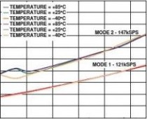
When operating the AD7997-1/AD7998-1 in Mode 1 and reading after conversion with a 3.4 MHz fSCL, the ADCs can achieve a typical throughput rate of up to 121 kSPS.

A
B
C
A conversion can be initiated on the AD7997/AD7998 by CONVSTis internally generated so no external clock is required, except when reading from or writing to the serial port. On the rising point A in Figure 32). The power-up time from shutdown mode CONVSTsignal must remain high for 1 μs for the part to power up fully. CONVST can be brought low after this time. This power-up time also includes the acquisition time of the ADC. The falling edge of the CONVSTmode; a conversion is also initiated at this point (point B in Figure 32). When the conversion is complete, approximately 2 μs later, the part returns to shutdown (point C in Figure 32) and remains there until the next rising edge of CONVSTmaster can then read the ADC to obtain the conversion result. The address pointer register must be pointing to the conversion result register in order to read back the conversion result.
Figure 32. Mode 1 Operation
Rev. 0 | Page 28 of 32
元器件交易网www.61k.com
AD7997/AD7998
Table 26 shows the channel selection in this mode via
Command Bits C4 to C1 in the address pointer register. The wake-up, acquisition, and conversion times combined should take approximately 3 μs. Following the write operation, the AD7997/AD7998 must be addressed again to indicate that a read operation is required. The read then takes place from the conversion result register. This read accesses the conversion result from the channel selected via the command bits. If
Command Bits C4 to C1 were set to 0111, and Bits D4 and D5 were set in the configuration register, a 4-byte read would be necessary. The first read accesses the data from the conversion on VIN1. While this read takes place, a conversion occurs on VIN2. The second read accesses this data from VIN2. Figure 34 illustrates how this mode operates; the user would first have written to the configuration register to select the sequence of channels to be converted before write addressing the part with the command bits set to 0111.
When operating the AD7997-1/AD7998-1 in Mode 2 with a high speed mode, 3.4 MHz SCL, the conversion may not be complete before the master tries to read the conversion result. If this is the case, the AD7997-1/AD7998-1 holds the SCL line low during the ACK clock after the read address, until the con-version is complete. When the conversion is complete, the AD7997-1/AD7998-1 releases the SCL line and the master can then read the conversion result.
After the conversion is initiated by setting the command bits in the address pointer byte, if the AD7997/AD7998 receives a STOP or NACK from the master, the AD7997/AD7998 stops converting.
MODE 2 – COMMAND MODE
This mode allows a conversion to be automatically initiated any time a write operation occurs. In order to use this mode, the Command Bits C4 to C1 in the address pointer byte shown in Table 7 must be programmed.
To select a single analog input for conversion in this mode, the user must set Bits C4 to C1 of the address pointer byte to indicate which channel to convert on (see Table 26). When all four command bits are 0, this mode is not in use.
To select a sequence of channels for conversion in this mode, first select the channels to be included in the sequence by setting the channel bits in the configuration register. Next, set the command bits in the address pointer byte to 0111. With the command bits of the address pointer byte set to 0111, the ADC knows to look in the configuration register for the sequence of channels to be converted. The ADC starts converting on the lowest channel in the sequence and then the next lowest until all the channels in the sequence are converted. The ADC stops converting the sequence when it receives a STOP bit.
Figure 29 illustrates a 2-byte read operation from the
conversion result register. This operation is preceded typically by a write to the address pointer register so that the following read accesses the desired register, in this case the conversion result register (see Figure 26). If Command Bits C4 to C1 are set when the contents of the address pointer register are being loaded, the AD7997/AD7998 begins to power up and convert upon the selected channel(s). Power-up begins on the fifth SCL falling edge of the address point byte, (see point A in Figure 33).
Table 26. Address Pointer Byte
C4 0 1 1 1 1 1 1 1 1 0
C3 0 0 0 0 0 1 1 1 1 1
C2 0 0 0 1 1 0 0 1 1 1
C1 0 0 1 0 1 0 1 0 1 1
P3 0 0 0 0 0 0 0 0 0 0
P2 0 0 0 0 0 0 0 0 0 0
P1 0 0 0 0 0 0 0 0 0 0
P0 0 0 0 0 0 0 0 0 0 0
Mode 2, Convert On Not selected VIN1 VIN2 VIN3 VIN4 VIN5 VIN6 VIN7 VIN8
Sequence of channels selected in the configuration register, Bits D11 to D4.
Comments
With the pointer Bits P3–P0 set to all 0s, the next read accesses the results of the conversion result register.
Rev. 0 | Page 29 of 32
元器件交易网www.61k.com
AD7997/AD7998
SCL
SDA
SCL
SDA
ACK BYAD7997/AD7998ACK BYMASTERNACK BYMASTER
03473-0-033
Figure 33. Mode 2 Operation
ACK BYACK BYACK BYACK BYRESULT FROM CH2
03473-0-034
RESULT FROM CH1
Figure 34. Mode 2 Sequence Operation
MODE 3—AUTOMATIC CYCLE INTERVAL MODE
An automatic conversion cycle can be selected and enabled by writing a value to the cycle timer register. A conversion cycle interval can be set up on the AD7997/AD7998 by programming the relevant bits in the 8-bit cycle timer register, as decoded in Table 24. Only the 3 LSBs are used to select the cycle interval; the 5 MSBs should contain 0s. When the 3 LSBs of the register are programmed with any configuration other than all 0s, a conversion takes place every X ms; the cycle interval, X, depends on the configuration of these three bits in the cycle timer register. There are seven different cycle time intervals to choose from, as shown in Table 24. Once the conversion has taken place, the part powers down again until the next conver-sion occurs. To exit this mode of operation, the user must
program the 3 LSBs of the cycle timer register to contain all 0s.
To select a channel(s) for operation in the cycle mode, set the corresponding channel bit(s), D11 to D4, of the configuration register. If more than one channel bit is set in the configuration register, the ADC automatically cycles through the channel sequence starting with the lowest channel and working its way up through the sequence. Once the sequence is complete, the ADC starts converting on the lowest channel again, continuing to loop through the sequence until the cycle timer register contents are set to all 0s. This mode is useful for monitoring signals, such as battery voltage and temperature, alerting only when the limits are violated.
Rev. 0 | Page 30 of 32
元器件交易网www.61k.com
AD7997/AD7998
OUTLINE DIMENSIONS

0.10
PLANE
COMPLIANT TO JEDEC STANDARDS MO-153AC
Figure 35. 20-Lead Thin Shrink Small Outline Package [TSSOP]
(RU-20)
Dimensions shown in millimeters
ORDERING GUIDE
Model1
AD7997BRU-0 AD7997BRU-0REEL AD7997BRUZ-03
AD7997BRUZ-0REEL3 AD7997BRU-1 AD7997BRU-1REEL AD7997BRUZ-13 AD7997BRUZ-1REEL3 AD7998BRU-0 AD7998BRU-0REEL AD7998BRUZ-03
AD7998BRUZ-0REEL3 AD7998BRU-1
AD7998BRU-1REEL AD7998BRUZ-13 AD7998BRUZ-1REEL3 EVAL-AD7997CB EVAL-AD7998CB
1
Temperature Range –40°C to +85°C –40°C to +85°C –40°C to +85°C –40°C to +85°C –40°C to +85°C –40°C to +85°C –40°C to +85°C –40°C to +85°C –40°C to +85°C –40°C to +85°C –40°C to +85°C –40°C to +85°C –40°C to +85°C –40°C to +85°C –40°C to +85°C –40°C to +85°C Linearity Error2(Max) ±0.5 LSB ±0.5 LSB ±0.5 LSB ±0.5 LSB ±0.5 LSB ±0.5 LSB ±0.5 LSB ±0.5 LSB ±1 LSB ±1 LSB ±1 LSB ±1 LSB ±1 LSB ±1 LSB ±1 LSB ±1 LSB Package Option RU-20 RU-20 RU-20 RU-20 RU-20 RU-20 RU-20 RU-20 RU-20 RU-20 RU-20 RU-20 RU-20 RU-20 RU-20 RU-20 Package Description TSSOP TSSOP TSSOP TSSOP TSSOP TSSOP TSSOP TSSOP TSSOP TSSOP TSSOP TSSOP TSSOP TSSOP TSSOP TSSOP
Standalone Evaluation Board Standalone Evaluation Board
The AD7997-0/AD7998-0 support standard and fast I2C interface modes. The AD7997-1/AD7998-1 support standard, fast, and high speed I2C interface modes. 2
Linearity error here refers to integral nonlinearity. 3
Z = Pb-free part.
RELATED PARTS IN I2C-COMPATIBLE ADC PRODUCT FAMILY
Part Number AD7994 AD7993 AD7992
Resolution Number of Input Channels
Package
16 TSSOP 16 TSSOP 10 MSOP
Rev. 0 | Page 31 of 32
元器件交易网www.61k.com
AD7997/AD7998
NOTES
Purchase of licensed I2C components of Analog Devices or one of its sublicensed Associated Companies conveys a license for the purchaser under the Philips I2C Patent Rights to use these components in an I2C system, provided that the system conforms to the I2C Standard Specification as defined by Philips.
? 2004 Analog Devices, Inc. All rights reserved. Trademarks and
registered trademarks are the property of their respective owners. D03473–0–9/04(0)

Rev. 0 | Page 32 of 32
二 : MAX6642_08中文资料
元器件交易网www.cecb2b.com
Temperature Sensor with Overtemperature Alarm

Features
The MAX6642 precise, two-channel digital temperature
sensor accurately measures the temperature of its ownoDual Channel: Measures Remote and LocalTemperature
die and a remote PN junction and reports the tempera-
ture data over a 2-wire serial interface. The remote PNo+0.25°C Resolution
junction is typically a substrate PNP transistor on theoHigh Accuracy ±1°C (max) (Remote) and die of a CPU, ASIC, GPU, or FPGA. The remote PN±2°C (Local) from +60°C to +100°C
junction can also be a discrete diode-connected small-
signal transistor.oMeasures Remote Temperature Up to +150°C
The 2-wire serial interface accepts standard systemoProgrammable Overtemperature AlarmTemperature Thresholds
management bus (SMBus?), Write Byte, Read Byte,
Send Byte, and Receive Byte commands to read theoSMBus/I2C-Compatible Interface
temperature data and to program the alarm thresholds.oTiny TDFN Package with Exposed PadTo enhance system reliability, the MAX6642 includes an
SMBus timeout. The temperature data format is 10 bitOrdering Informationwith the least significant bit (LSB) corresponding to
+0.25°C. The ALERToutput asserts when the local orremote overtemperature thresholds are violated. A faultqueue may be used to prevent the ALERToutput from
setting until two consecutive faults have been detected.Measurements can be done autonomously or in a sin-
gle-shot mode.Remote accuracy is ±1°C maximum error between+60°C and +100°C. The MAX6642 operates from -40°Cto +125°C, and measures remote temperaturesbetween 0°C and +150°C. The MAX6642 is available ina 6-pin TDFN package with an exposed pad.*EP = Exposed pad.
Desktop ComputersPin Configuration and Functional Diagram appear at end ofNotebook Computersdata sheet.
Servers
Thin ClientsTest and Measurement
WorkstationsGraphic Cards
Maxim Integrated Products1
For pricing, delivery, and ordering information, please contact Maxim Direct at 1-888-629-4642,or visit Maxim’s website at www.maxim-ic.com.MAX6642

6642 MAX6642_08中文资料
元器件交易网www.cecb2b.com
±1°C, SMBus-Compatible Remote/Local
Temperature Sensor with Overtemperature AlarmMAX6642
ABSOLUTE MAXIMUM RATINGS
All Voltages Referenced to GND
VCC...........................................................................-0.3V to +6VDXP.............................................................-0.3V to (VCC+ 0.3V)SCLK, SDA, ALERT..................................................-0.3V to +6VSDA, ALERTCurrent...........................................-1mA to +50mAContinuous Power Dissipation (TA= +70°C)
6-Pin TDFN (derate 24.4mW/°C above +70°C).........1951mW
ESD Protection (all pins, Human Body Model)................±2000VJunction Temperature......................................................+150°COperating Temperature Range.........................-40°C to +125°CStorage Temperature Range.............................-65°C to +150°CLead Temperature (soldering, 10s).................................+300°C
Stresses beyond those listed under “Absolute Maximum Ratings” may cause permanent damage to the device. These are stress ratings only, and functionaloperation of the device at these or any other conditions beyond those indicated in the operational sections of the specifications is not implied. Exposure toabsolute maximum rating conditions for extended periods may affect device reliability.
ELECTRICAL CHARACTERISTICS
2_______________________________________________________________________________________
6642 MAX6642_08中文资料
元器件交易网www.cecb2b.com
Temperature Sensor with Overtemperature Alarm±1°C, SMBus-Compatible Remote/LocalELECTRICAL CHARACTERISTICS (continued)
Note 2:Timing specifications guaranteed by design.
Note 3:The serial interface resets when SCLK is low for more than tTIMEOUT.
Note 4:A transition must internally provide at least a hold time to bridge the undefined region (300ns max) of SCLK’s falling edge.
_______________________________________________________________________________________3
MAX6642
6642 MAX6642_08中文资料 扩展:max232中文资料 / max485中文资料 / max3232中文资料
元器件交易网www.cecb2b.com
±1°C, SMBus-Compatible Remote/LocalTemperature Sensor with Overtemperature Alarm42(VCC= 3.3V, TA= +25°C, unless otherwise noted.)
66XAM
4STANDBY SUPPLY CURRENTREMOTE TEMPERATURE ERRORvs. CLOCK FREQUENCYvs. REMOTE-DIODE TEMPERATURE

5.0120cot 24.5466XAM1))CA4.0°(μ (R TO0NRE3.5RRE REURC3.0U-1 TYLAPREP2.5UP-2SM2.0ET1.5-31.0-40.010.11101000255075100125CLOCK FREQUENCY (kHz)TEMPERATURE (°C)LOCAL TEMPERATURE ERRORTEMPERATURE ERRORvs. DIE TEMPERATURE

vs. POWER-SUPPLY NOISE FREQUENCY
32.01.52))C°C(°( R OR1.0R1ORRER EE RE0.5U0RTUATRAER0PEM-1PEMTET-0.5-2-1.0-3-1.502550751001250.00010.0010.010.1110100TEMPERATURE (°C)FREQUENCY (kHz)TEMPERATURE ERROR
TEMPERATURE ERROR vs. DXP NOISE FREQUENCYvs. DXP-GND CAPACITANCE1002.060co90t 24661.0XAM)80C)°C( °0R70( ORRORR-1.0E60 REE REU50R-2.0TUATRAE40PRE-3.0MPE30MTE20T-4.010-5.00-6.00.0010.010.11101000.1110100FREQUENCY (kHz)DXP-GND CAPACITANCE (nF)_______________________________________________________________________________________
6642 MAX6642_08中文资料
元器件交易网www.cecb2b.com
Temperature Sensor with Overtemperature Alarm±1°C, SMBus-Compatible Remote/Local
Detailed Descriptionremote temperature is measured eight times per sec-
The MAX6642 is a temperature sensor for localond. The results of the previous conversion are alwaysand remote temperature-monitoring applications.available, even if the ADC is busy.
Communication with the MAX6642 occurs through the
SMBus-compatible serial interface and dedicated alertLow-Power Standby Modepins. ALERTasserts if the measured local or remoteStandby mode reduces the supply current to less thantemperature is greater than the software-programmed10μA by disabling the ADC and timing circuitry. EnterALERTlimit.standby mode by setting the RUNbit to 1 in the config-
uration byte register (Table 4). All data is retained in
The MAX6642 converts temperatures to digital datamemory, and the SMBus interface is active and listen-either at a programmed rate of eight conversions pering for SMBus commands. Standby mode is not a shut-second or in single conversions. Temperature data isdown mode. With activity on the SMBus, the devicerepresented by 8 data bits (at addresses 00h and 01h),draws more supply current (see the Typical Operatingwith the LSB equal to +1°C and the MSB equal toCharacteristics). In standby mode, the MAX6642 can+128°C. Two additional bits of remote temperature databe forced to perform ADC conversions through theare available in the “extended” register at address 10hone-shot command, regardless of the RUNbit status.and 11h (Table 2) providing resolution of +0.25°C.If a standby command is received while a conversion is
ADC and Multiplexerin progress, the conversion cycle is truncated, and the
The averaging ADC integrates over a 60ms perioddata from that conversion is not latched into a tempera-(each channel, typ), with excellent noise rejection.ture register. The previous data is not changed andThe multiplexer automatically steers bias currentsremains available.
through the remote and local diodes. The ADC andSupply-current drain during the 125ms conversion peri-associated circuitry measure each diode’s forward volt-od is 500μA (typ). In standby mode, supply currentage and compute the temperature based on this volt-drops to 3μA (typ).
age. Both channels are automatically converted once
the conversion process has started, either in free-run-SMBus Digital Interfacening or single-shot mode. If one of the two channels isFrom a software perspective, the MAX6642 appears asnot used, the device still performs both measurements,a set of byte-wide registers that contain temperatureand the user can ignore the results of the unused chan-data, alarm threshold values, and control bits. A stan-nel. If the remote-diode channel is unused, connectdard SMBus-compatible 2-wire serial interface is usedDXP to GND rather than leaving DXP open.to read temperature data and write control bits and
alarm threshold data.
The conversion time per channel (remote and internal)
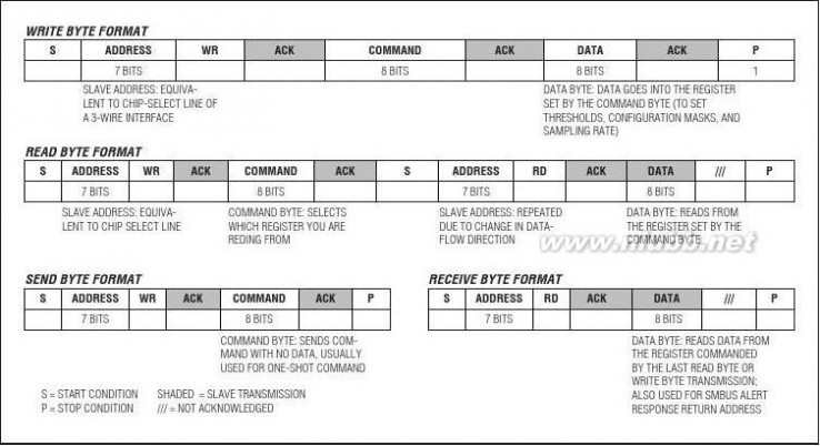
is 125ms. If both channels are being used, then eachThe MAX6642 employs four standard SMBus protocols:channel is converted four times per second. If theWrite Byte, Read Byte, Send Byte, and Receive Byte.external conversion-only option is selected, then the(Figures 1, 2, and 3). The shorter Receive Byte protocol
allows quicker transfers, provided that the correct data
扩展:max232中文资料 / max485中文资料 / max3232中文资料
_______________________________________________________________________________________5
MAX6642
6642 MAX6642_08中文资料
元器件交易网www.cecb2b.com
±1°C, SMBus-Compatible Remote/Local
Temperature Sensor with Overtemperature AlarmMAX6642
register was previously selected by a Write Byteinstruction. Use caution when using the shorter proto-cols in multimaster systems, as a second master couldoverwrite the command byte without informing the firstmaster.
Read temperature data from the read internal tempera-ture (00h) and read external temperature (01h) regis-ters. The temperature data format for these registers is8 bits for each channel, with the LSB representing +1°C(Table 1).
Read the additional bits from the read extended tem-perature byte register (10h, 11h), which extends thedata to 10 bits and the resolution to +0.25°C per LSB(Table 2).

Figure 1. SMBus Protocols
Figure 2. SMBus Write Timing Diagram6
_______________________________________________________________________________________
6642 MAX6642_08中文资料
元器件交易网www.cecb2b.com
Temperature Sensor with Overtemperature Alarm±1°C, SMBus-Compatible Remote/LocalWhen a conversion is complete, the main temperature
register and the extended temperature register areTable 1. Main Temperature Register updated. (High Byte) Data Format
Alarm Threshold RegistersTwo registers store ALERTthreshold values—one eachfor the local and remote channels. If either measuredtemperature equals or exceeds the corresponding
ALERTthreshold value, the ALERTinterrupt assertsunless the ALERTbit is masked.The power-on-reset (POR) state of the local ALERTTHIGHregister is +70°C (0100 0110). The POR state ofthe remote ALERTTHIGHregister is +120°C (0111 1000).Diode Fault DetectionA continuity fault detector at DXP detects an open cir-
cuit on DXP, or a DXP short to VCCor GND. If an openTemperature Register (Low Byte) Dataor short circuit exists, the external temperature registerFormat
is loaded with 1111 1111 and status bit 2 (OPEN) of the
status byte is set to 1. Immediately after POR, the statusregister indicates that no fault is present. If a fault ispresent upon power-up, the fault is not indicated untilthe end of the first conversion. Diode faults do not set
the ALERToutput.ALERTInterrupts
The ALERTinterrupt occurs when the internal or externalture is above the trip threshold, write a new high limit thattemperature reading exceeds a high temperature limitis higher than the current temperature. The ALERToutput(user programmed). The ALERTinterrupt output signal isis open drain, allowing multiple devices to share a com-latched and can be cleared only by reading the statusmon interrupt line.
register after the fault condition no longer exists or byAlert Response Addresssuccessfully responding to the alert response address. IfThe SMBus alert response interrupt pointer providesthe ALERTis cleared by responding to the alertquick fault identification for simple slave devices likeresponse address and the temperature fault conditiontemperature sensors. Upon receiving an ALERTinter-still exists, ALERTis reasserted after the next tempera-rupt signal, the host master can broadcast a Receiveture-monitoring cycle. To clear ALERTwhile the tempera-Byte transmission to the alert response slave address
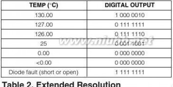
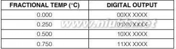
Figure 3. SMBus Read Timing Diagram
_______________________________________________________________________________________7
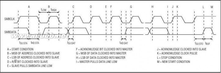
MAX6642
6642 MAX6642_08中文资料
元器件交易网www.cecb2b.com
±1°C, SMBus-Compatible Remote/Local
Temperature Sensor with Overtemperature AlarmMAX6642
Table 3. Command-Byte Assignments
(0001 100). Following such a broadcast, any slave
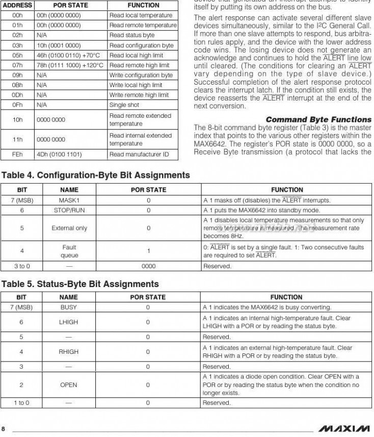
6642 MAX6642_08中文资料
元器件交易网www.cecb2b.com
Temperature Sensor with Overtemperature Alarm

±1°C, SMBus-Compatible Remote/Localcommand byte) that occurs immediately after PORPOR and UVLOreturns the current local temperature data.To prevent ambiguous power-supply conditions from
扩展:max232中文资料 / max485中文资料 / max3232中文资料
Single-Shotcorrupting the data in memory and causing erratic
The single-shot command immediately forces a newbehavior, a POR voltage detector monitors Vconversion cycle to begin. If the single-shot commandclears the memory if VCCandis received while the MAX6642 is in standby modepower is first applied and VCCfalls below 2.1 (typ). When
CCrises above 2.1 (typ),
(RUNbit = 1), a new conversion begins, after which thethe logic blocks begin operating, although reads anddevice returns to standby mode. If a single-shot con-writes at V
version is in progress when a single-shot command issecond VCClevels below 3V are not recommended. Areceived, the command is ignored. If a single-shot(UVLO) comparator prevents the ADC from convertingCCcomparator, the ADC undervoltage lockoutcommand is received in autonomous mode (RUNbit =until there is sufficient headroom (VCC= +2.7V typ).0), the command is ignored.Power-Up Defaults
Configuration Byte FunctionsPower-up defaults include:
The configuration byte register (Table 4) is a read-write?ALERToutput is cleared.
register with several functions. Bit 7 is used to mask?ADC begins autoconverting at a 4Hz rate.(disable) interrupts. Bit 6 puts the MAX6642 into stand-
by mode (STOP) or autonomous (RUN) mode. Bit 5 dis-?Command byte is set to 00h to facilitate quickables local temperature conversions for faster (8Hz)local Receive Byte queries.
remote temperature monitoring. Bit 4 prevents setting?Local (internal) THIGHlimit set to +70°C.
the ALERToutput until two consecutive measurements?Remote (external) THIGHlimit set to +120°C.result in fault conditions.Status Byte Functions
The status byte register (Table 5) indicates which (ifRemote-Diode Selectionany) temperature thresholds have been exceeded. ThisThe MAX6642 can directly measure the die temperaturebyte also indicates whether the ADC is converting andof CPUs and other ICs that have on-board temperature-whether there is an open-circuit fault detected on thesensing diodes (see the Typical Operating Circuit) orexternal sense junction. After POR, the normal state ofthey can measure the temperature of a discrete diode-all flag bits is zero, assuming no alarm conditions areconnected transistor.
present. The status byte is cleared by any successful
read of the status byte after the overtemperature faultEffect of Ideality Factorcondition no longer exists.The accuracy of the remote temperature measurements
depends on the ideality factor (n) of the remote “diode”
Slave Addresses(actually a transistor). The MAX6642 is optimized for n
The MAX6642 has eight fixed addresses available.= 1.008, which is the typical value for the Intel PentiumThese are shown in Table 6.III. A thermal diode on the substrate of an IC is normallyThe MAX6642 also responds to the SMBus alerta PNP with its collector grounded. Connect the anoderesponse slave address (see the Alert Response(emitter) to DXP and the cathode to GND of theAddresssection).MAX6642.
If a sense transistor with an ideality factor other than
1.008 is used, the output data is different from the data
obtained with the optimum ideality factor. Fortunately,the difference is predictable.
Assume a remote-diode sensor designed for a nominal
ideality factor n
perature of a diode with a different ideality factor nNOMINALis used to measure the tem-1.

9MAX6642
6642 MAX6642_08中文资料
元器件交易网www.cecb2b.com
±1°C, SMBus-Compatible Remote/Local
Temperature Sensor with Overtemperature AlarmMAX6642
where temperature is measured in Kelvin andnNOMIMALfor the MAX6642 is 1.008.
As an example, assume you want to use the MAX6642with a CPU that has an ideality factor of 1.002. If thediode has no series resistance, the measured data is


For a real temperature of +85°C (358.15K), the mea-sured temperature is +82.91°C (356.02K), an error of
-2.13°C.
Table 7. Remote-Sensor TransistorDiscrete Remote Diodes
When the remote-sensing diode is a discrete transistor,connect its collector and base together. Table 7 listsexamples of discrete transistors that are appropriate foruse with the MAX6642.
The transistor must be a small-signal type with a rela-tively high forward voltage; otherwise, the A/D inputvoltage range can be violated. The forward voltage atthe highest expected temperature must be greater than0.25V at 10μA, and at the lowest expected tempera-ture, the forward voltage must be less than 0.95V at100μA. Large power transistors must not be used. Also,ensure that the base resistance is less than 100?. Tightspecifications for forward current gain (50 < ? <150, forexample) indicate that the manufacturer has goodprocess controls and that the devices have consistentVBEcharacteristics.
扩展:max232中文资料 / max485中文资料 / max3232中文资料
Manufacturers of discrete transistors do not normallyspecify or guarantee ideality factor. This is normally nota problem since good-quality discrete transistors tendto have ideality factors that fall within a relatively narrowrange. We have observed variations in remote tempera-ture readings of less than ±2°C with a variety of dis-crete transistors. Still, it is good design practice toverify good consistency of temperature readings withseveral discrete transistors from any manufacturerunder consideration.
Effect of Series Resistance
Series resistance in a sense diode contributes addition-al errors. For nominal diode currents of 10μA and100μA, the change in the measured voltage due toseries resistance is:
?VM= RS (100μA - 10μA) = 90μA ??RS
Since +1°C corresponds to 198.6μV, series resistancecontributes a temperature offset of:
Assume that the diode being measured has a seriesresistance of 3?. The series resistance contributes anoffset of:

The effects of the ideality factor and series resistanceare additive. If the diode has an ideality factor of 1.002and series resistance of 3?, the total offset can be cal-culated by adding error due to series resistance witherror due to ideality factor:
1.36°C - 2.13°C = -0.77°C
for a diode temperature of +85°C.
In this example, the effect of the series resistance andthe ideality factor partially cancel each other.
10
ADC Noise Filtering
The integrating ADC used has good noise rejection forlow-frequency signals such as 60Hz/120Hz power-sup-ply hum. In noisy environments, high-frequency noisereduction is needed for high-accuracy remote mea-surements. The noise can be reduced with careful PCBlayout and proper external noise filtering.
High-frequency EMI is best filtered at DXP with anexternal 2200pF capacitor. Larger capacitor values canbe used for added filtering, but do not exceed 3300pFbecause excessive capacitance can introduce errors
______________________________________________________________________________________
6642 MAX6642_08中文资料
元器件交易网www.cecb2b.com
Temperature Sensor with Overtemperature Alarm±1°C, SMBus-Compatible Remote/Localdue to the rise time of the switched current source.9)Copper cannot be used as an EMI shield; only fer-Nearly all noise sources tested cause the temperaturerous materials such as steel work well. Placing aconversion results to be higher than the actual temper-copper ground plane between the DXP-DXN tracesature, typically by +1°C to +10°C, depending on theand traces carrying high-frequency noise signalsfrequency and amplitude (see the Typical Operatingdoes not help reduce EMI.
Characteristics).Twisted-Pair and Shielded Cables
PCB LayoutUse a twisted-pair cable to connect the remote sensor
Follow these guidelines to reduce the measurementfor remote-sensor distances longer than 8in or in veryerror of the temperature sensors:noisy environments. Twisted-pair cable lengths can be
1)Connect the thermal-sense diode to the MAX6642between 6ft and 12ft before noise introduces excessiveusing two traces—one between DXP and theerrors. For longer distances, the best solution is aanode, the other between the MAX6642’s GND andshielded twisted pair like that used for audio micro-the cathode. Do not connect the cathode to GND atphones. For example, Belden #8451 works well for dis-the sense diode.tances up to 100ft in a noisy environment. At the
2)Place the MAX6642 as close as is practical to thedevice, connect the twisted pair to DXP and GND andremote thermal diode. In noisy environments, suchthe shield to GND. Leave the shield unconnected at theas a computer motherboard, this distance can beremote diode.
4in to 8in (typ). This length can be increased if theFor very long cable runs, the cable’s parasitic capaci-worst noise sources are avoided. Noise sourcestance often provides noise filtering, so the 2200pFinclude CRTs, clock generators, memory buses,capacitor can often be removed or reduced in value.and ISA/PCI buses.Cable resistance also affects remote-sensor accuracy.
3)Do not route the thermal diode lines next to theFor every 1?of series resistance, the error is approxi-deflection coils of a CRT. Also, do not route themately 1/2°C.
traces across fast digital signals, which can easilyThermal Mass and Self-Heatingintroduce a 30°C error, even with good filtering.When sensing local temperature, this device is intend-
4)Route the thermal diode traces in parallel and ined to measure the temperature of the PCB to which it isclose proximity to each other, away from any highersoldered. The leads provide a good thermal pathvoltage traces, such as +12VDC. Leakage currentsbetween the PCB traces and the die. Thermal conduc-from PCB contamination must be dealt with careful-tivity between the die and the ambient air is poor byly since a 20M?leakage path from DXP to groundcomparison, making air temperature measurementscauses about +1°C error. If high-voltage traces areimpractical. Because the thermal mass of the PCB is farunavoidable, connect guard traces to GND ongreater than that of the MAX6642, the device followseither side of the DXP trace (Figure 4).temperature changes on the PCB with little or no per-
扩展:max232中文资料 / max485中文资料 / max3232中文资料
5)Route through as few vias and crossunders as pos-ceivable delay.
sible to minimize copper/solder thermocoupleWhen measuring temperature of a CPU or other IC witheffects.an on-chip sense junction, thermal mass has virtually
6)When introducing a thermocouple, make sure thatno effect; the measured temperature of the junctionboth the thermal diode paths have matching ther-
mocouples. A copper-solder thermocouple exhibits
3μV/°C, and it takes about 200μV of voltage error atDXP to cause a +1°C measurement error. Adding afew thermocouples causes a negligible error.7)Use wide traces. Narrow traces are more inductive
and tend to pick up radiated noise. The 10-milwidths and spacing recommended in Figure 4 arenot absolutely necessary, as they offer only a minorimprovement in leakage and noise over narrow
traces. Use wider traces when practical.8)Add a 47?resistor in series with V
Typical Operating CircuitCCfor best noise
filtering (see the ).Figure 4. Recommended DXP PC Traces
______________________________________________________________________________________11
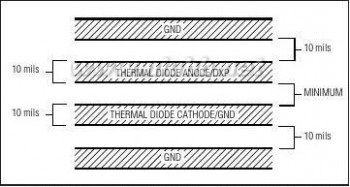
MAX6642
6642 MAX6642_08中文资料
元器件交易网www.cecb2b.com
±1°C, SMBus-Compatible Remote/Local
Temperature Sensor with Overtemperature Alarm
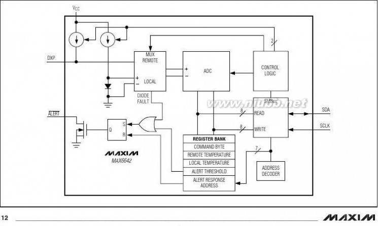
MAX6642
tracks the actual temperature within a conversion cycle.When measuring temperature with discrete remote sen-sors, smaller packages, such as SOT23s, yield the bestthermal response times. Take care to account for ther-mal gradients between the heat source and the sensor,and ensure that stray air currents across the sensorpackage do not interfere with measurement accuracy.Self-heating does not significantly affect measurementaccuracy. Remote-sensor self-heating due to the diodecurrent source is negligible. For the local diode, theworst-case error occurs when autoconverting at thefastest rate and simultaneously sinking maximum cur-rent at the ALERToutput. For example, with VCC =+5.0V, at an 8Hz conversion rate and with ALERTsink-ing 1mA, the typical power dissipation is:
5.0V x 450μA + 0.4V x 1mA = 2.65mW
?J-A for the 6-pin TDFN package is about +41°C/W, soassuming no copper PCB heat sinking, the resultingtemperature rise is:
?T = 2.65mW x 41°C/W = +0.11°C
Even under nearly worst-case conditions, it is difficult tointroduce a significant self-heating error.
Chip Information
PROCESS: BiCMOS
Functional Diagram
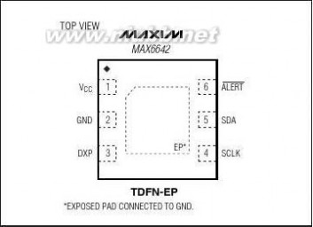
6642 MAX6642_08中文资料
元器件交易网www.cecb2b.com
Temperature Sensor with Overtemperature Alarm±1°C, SMBus-Compatible Remote/Local
Package Information
For the latest package outline information and land patterns, go
to .

______________________________________________________________________________________13MAX6642
6642 MAX6642_08中文资料
元器件交易网www.cecb2b.com
±1°C, SMBus-Compatible Remote/LocalTemperature Sensor with Overtemperature AlarmMAX6642

Maxim cannot assume responsibility for use of any circuitry other than circuitry entirely embodied in a Maxim product. No circuit patent licenses areimplied. Maxim reserves the right to change the circuitry and specifications without notice at any time.
14____________________Maxim Integrated Products, 120 San Gabriel Drive, Sunnyvale, CA 94086 408-737-7600?2008 Maxim Integrated Products is a registered trademark of Maxim Integrated Products, Inc.
扩展:max232中文资料 / max485中文资料 / max3232中文资料
三 : CLL5252A中文资料
元器件交易网www.cecb2b.com
Continental Device India Limited
An ISO/TS 16949, ISO 9001 and ISO 14001 Certified Company
SILICON ZENER DIODES CLL5230A - CLL5261A
Hermetically Sealed Glass Silicon Zener Diodes
SOD-80C Zener Diodes
CLL5230A to CLL5261A, 500mW Hermetically Sealed, Glass Silicon Zener Diodes
Maximum Ratings
Ratings
DC Power Dissipation @ TA ≤ 50°CDerate above TA = 50°COperating and Storage JunctionTemperature Range
SymbolPDTJ – Tstg
Value5003.3– 65 to + 200
UnitmWmW/°C° C
Electrical Characteristics
TA = 25°C Unless otherwise noted Based on dc measurements at thermal equilibrium; case temperature maintained at30 ± 2°C. VF = 1.1 max @ IF = 200 mA for all types.
NominalTestMax Zener ImpedanceMax Reverse Leakage CurrentZener VoltageCurrentA and B Suffix onlyA and B Suffix onlyNon-Suffix
IZTVZ @ IZT
VoltsmAZZT @ IZTZZK @ IZKIR@V

R

I

R @ VR(Note 2)(Note 2)Ohms= 0.25 mAμAUsed for
OhmsABSuffix A μA
4.7
5.15.66.06.26.87.58.28.79.110.011.012.013.014.015.016.017.0
202020202020202020202020209.59.08.57.87.4
191711775688101722301315161719
19001600160016001000750500500600600600600600600600600600600
5.05.05.05.05.03.03.03.03.03.03.02.01.00.50.10.10.10.1
1.91.92.93.33.84.85.76.26.26.77.68.08.79.49.510.511.412.4
2.02.03.03.54.05.06.06.56.57.08.08.49.19.910.011.012.013.0
505050505030303030303030101010101010
Max ZenerVoltageTemperatureCoeff. (A and BSuffix only)θ VZ (%/°C)
± 0.030± 0.030+ 0.038+ 0.038+ 0.045+ 0.050+ 0.058+ 0.062+ 0.065+ 0.068+ 0.075+ 0.076+ 0.077+ 0.079+ 0.082+ 0.082+ 0.083+ 0.084
Type No.(Note 1)
CLL5230ACLL5231ACLL5232ACLL5233ACLL5234ACLL5235ACLL5236ACLL5237ACLL5238ACLL5239ACLL5240ACLL5241ACLL5242ACLL5243ACLL5244ACLL5245ACLL5246ACLL5247A
CLL5230ARev290001????
Continental Device India Limited Data Sheet Page 1 of 4
5252a CLL5252A中文资料
元器件交易网www.cecb2b.com
Electrical Characteristics
SOD-80C Zener Diodes, 500 mW
TA = 25°C Unless otherwise noted Based on dc measurements at thermal equilibrium; case temperature maintained at30 ± 2°C. VF = 1.1 max @ IF = 200 mA for all types.
NominalTestMax Zener ImpedanceMax Reverse Leakage CurrentZener VoltageCurrentA and B Suffix onlyA and B Suffix onlyNon-SuffixVZ @ IZTIZTVoltsmAZZT @ IZTZZK @ IZKIR@VRIR @ VR(Note 2)(Note 2)Ohms= 0.25 mAμAVoltsUsed for
OhmsABSuffix A μA
18.0
19.020.022.024.025.027.028.030.033.036.039.043.047.0
7.06.66.25.65.25.04.64.54.23.83.43.23.02.7
21232529333541444958708093105
6006006006006006006006006007007008009001000
0.10.10.10.10.10.10.10.10.10.10.10.10.10.1
13.313.314.316.217.118.120.020.022.024.026.029.031.034.0
14.014.015.017.018.019.021.021.023.025.027.030.033.036.0Note 2
1010101010101010101010101010
Max ZenerVoltageTemperatureCoeff. (A and BSuffix only)θ VZ (%/°C)
+ 0.085+ 0.086+ 0.086+ 0.087+ 0.088+ 0.089+ 0.090+ 0.091+ 0.091+ 0.092+ 0.093+ 0.094+ 0.095+0.095
Type No.(Note 1)
CLL5248ACLL5249ACLL5250ACLL5251ACLL5252ACLL5253ACLL5254ACLL5255ACLL5256ACLL5257ACLL5258ACLL5259ACLL5260ACLL5261A
Polarity:Cathode indicated by colour band.
Note 1:Suffix A for ± 10% tolerance; Suffix B for ± 5% tolerance.
CLL5230ARev290001????
:Pulse test : 20ms ≤ tp ≤ 50ms.
Continental Device India Limited Data Sheet Page 2 of 4
5252a CLL5252A中文资料
元器件交易网www.cecb2b.com
CLL5230A - CLL5261A
SOD - 80C
Mini MELF (LL-34)
SOD 80C (LL-34) Mini MELF Hermetically Sealed Glass Package
De-reeling directionAll Dimensions are in mm
Notes:
1.Maximum of 0.5% of the total number of components per reel may be missing-exclusively at the beginning and at the end of the reel.
2.A maximum of three consecutive components may be missing, provided this gap is followed by six consecutive components.
De-reeling direction
All Dimensions are in mm
Drawings are not to scale
Packing Detail
PACKAGE
STANDARD PACKINNER CARTON BOX
DetailsNet Weight/QtySizeQty
SOD-80C T&R2.5K/reel225 gm/2.5K pcs9" x 9" x 9"40K
CLL5230ARev290001????
OUTER CARTON BOX
SizeQtyGr Wt18" x 12" x 10"80K7.2 kgs19" x 19" x 20"320K28.8 kgs
Continental Device India Limited Data Sheet Page 3 of 4
5252a CLL5252A中文资料
元器件交易网www.cecb2b.com
扩展:stc12c5a60s2中文资料 / 8205a中文资料 / sim900a中文资料
Component Disposal Instructions
1. CDIL Semiconductor Devices are RoHS compliant, customers are requested to please dispose
as per prevailing Environmental Legislation of their Country. CLL5230A - CLL5261A SOD - 80C Mini MELF (LL-34)
2. In Europe, please dispose as per EU Directive 2002/96/EC on Waste Electrical and Electronic Equipment (WEEE).
Customer Notes
Disclaimer
TheproductinformationandtheselectionguidesfacilitateselectionoftheCDIL'sSemiconductorDevice(s)bestsuitedforapplicationinyourproduct(s)asperyourrequirement.ItisrecommendedthatyoucompletelyreviewourDataSheet(s)soastoconfirmthattheDevice(s)meetfunctionalityparametersforyourapplication.TheinformationfurnishedintheDataSheetandontheCDILWebSite/CDarebelievedtobeaccurateandreliable.CDILhowever,doesnotassumeresponsibilityforinaccuraciesorincompleteinformation.Furthermore,CDILdoesnotassumeliabilitywhatsoever,arisingoutoftheapplicationoruseofanyCDILproduct;neitherdoesitconveyanylicenseunderitspatentrightsnorrightsofothers.Theseproductsarenotdesignedforuseinlifesaving/supportappliancesorsystems.CDILcustomerssellingtheseproducts(eitherasindividualDiscreteSemiconductorDevicesorincorporatedintheirendproducts),inanylifesaving/supportappliancesorsystemsorapplicationsdosoattheirownriskandCDILwillnotberesponsibleforanydamages resulting from such sale(s).
CDIL strives for continuous improvement and reserves the right to change the specifications of its products without prior notice.
CDIL is a registered Trademark of
Continental Device India Limited
C-120 Naraina Industrial Area, New Delhi 110 028, India.
Telephone + 91-11-2579 6150, 4141 1112 Fax + 91-11-2579 5290, 4141 1119

email@cdil.com www.cdilsemi.com
CLL5230ARev290001????
Continental Device India Limited Data Sheet Page 4 of 4
扩展:stc12c5a60s2中文资料 / 8205a中文资料 / sim900a中文资料
四 : KPY55RK中文资料

元器件交易网www.cecb2b.com
Silicon PiezoresistiveRelative Pressure Sensor
KPY 51-RK

KPY 57-RK
Features????
Low pressure and temperature hysteresisFast response
High sensitivity and linearity
Fatigue free monocrystaline silicon diaphragmgiving high load cycle stability?High long term stability
?Built in silicon temperature sensor
?Provided for further fabrication, protection cap
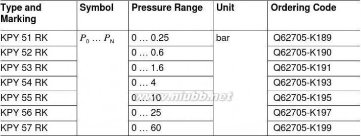
Pin Configuration
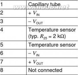
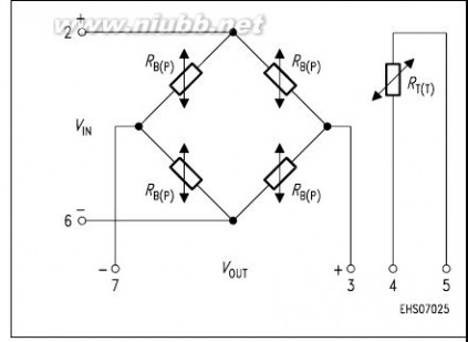
Semiconductor Group102.97
55rk KPY55RK中文资料
元器件交易网www.cecb2b.com
KPY 51-RKKPY 57-RK
Absolute Maximum Ratings

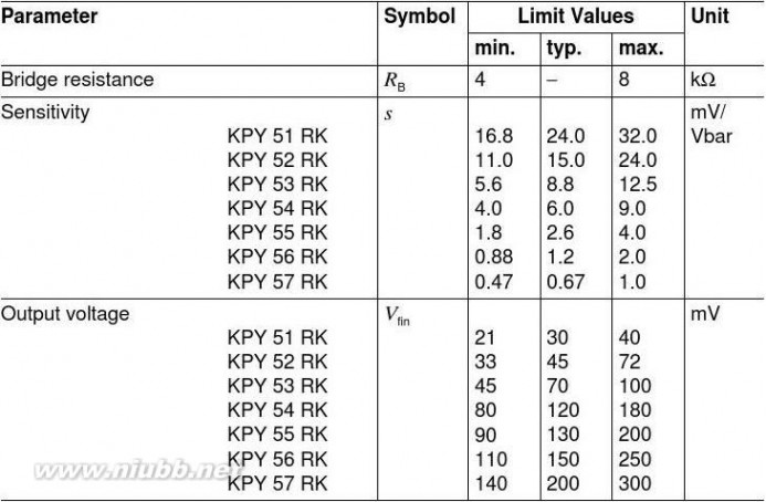
1)Frontside coupling applies pressure onto chip face.
Rearside coupling applies pressure through Kovar centre tube.
Electrical Characteristics
atT = 25 ?C andV = 5 V, unless otherwise specified.Semiconductor Group

2
55rk KPY55RK中文资料
元器件交易网www.cecb2b.com
KPY 51-RKKPY 57-RK
Electrical Characteristics(cont’d)
atT = 25 ?C andV = 5 V, unless otherwise specified.
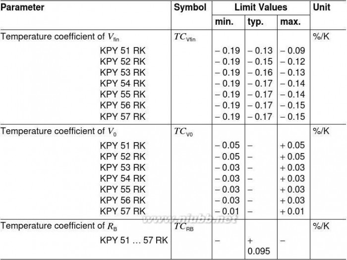
Electrical Characteristics
atT = 25 ?C,T = 125 ?C,T = 25 ?C andV = 5 V, unless otherwise specified.Semiconductor Group

3
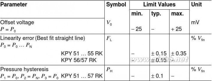
55rk KPY55RK中文资料
元器件交易网www.cecb2b.com
KPY 51-RKKPY 57-RK
Electrical Characteristics(cont’d)
atT = 25 ?C,T = 125 ?C,T = 25 ?C andV = 5 V, unless otherwise specified.Package Outline
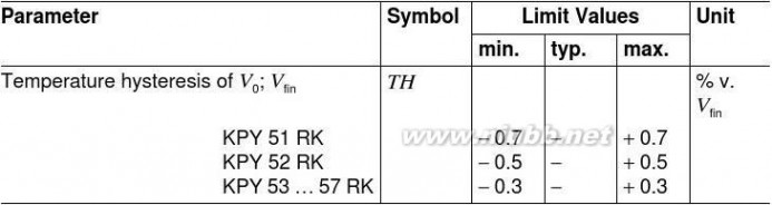
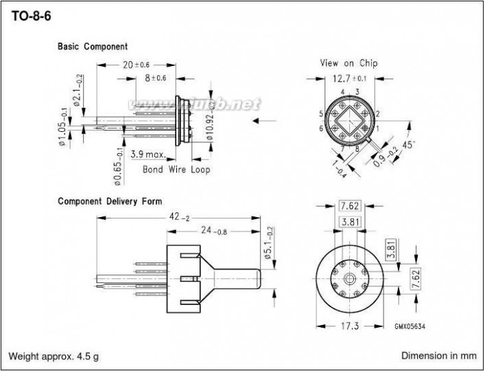
Exterior Packaging
I.e. tubes, trays, boxes are shown in our Data Book “Package Information”.Semiconductor Group

4
扩展:tl431中文资料 / ds18b20中文资料 / lm358中文资料
本文标题:中文资料-AD7998BRUZ-0REEL3中文资料61阅读| 精彩专题| 最新文章| 热门文章| 苏ICP备13036349号-1