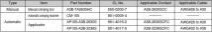
一 : A4B-15PA-2DS中文资料

元器件交易网www.61k.com
sFeatures
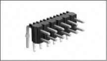
1. Miniature Type and High Density Mounting
These connectors are designed in a miniature and lightweight product, and mounted in the high density. Thecrimping case is structured in the 2mm pitch grid, so thatconnectors can be arranged for use.
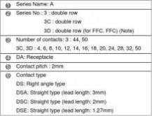
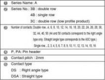
2. Variation in Number of Contacts
In addition to the dip type, SMT and crimping types areavailable with broad variations.
3. Stacking Variation
When the connector is used for board to board, set 6mmbetween boards in conjunction with the pin header A3B,or 5.1mm between boards in conjunction with the pin

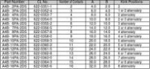
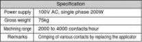
sProduct Specifications
header A3C.

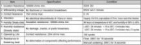
Note 1: Includes temperature rise caused by current flow.
Note 2: The term "storage" refers to products stored for long period of time prior to mounting and use. Operating Temperature
Range and Humidity range covers non conducting condition of installed connectors in storage, shipment or duringtransportation.
sApplications
VTR, vehicle telephones, and other various kinds of electronic equipment
sMaterial
C10

元器件交易网www.61k.com
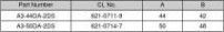
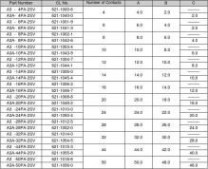
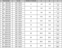
sOrdering Information
qPin Header (DIP type)
qReceptacle (DIP type)
A 3 - 44 D - 2 DS


qCrimping Socket


C11


元器件交易网www.61k.com
qCrimping Contact
A 3B - 2630 SCFC
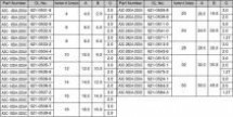
q Pin Header (SMT type)
qReceptacle (SMT type)
C12


元器件交易网www.61k.com
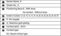
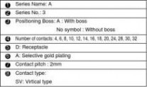
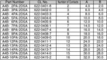
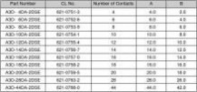
sPin Header
qA3B Straight Type
2±0.05

BPCB mounting pattern
B±0.12±0.05
0.1
?0.8+_1
qA3B Right Angle Type

BPCB mounting pattern
B±0.12±0.05
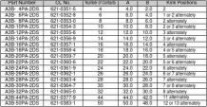
Note 1. Please order the product per 100 pcs.
Note 2. Diameter of 28 or more contacts is ?0.95±0.04.
2±0.05
Note 3C13


元器件交易网www.61k.com
qA4B Straight Type

BPCB mounting pattern??????????????????????????????Note: Please order the product per 100 pcs.qA4B Right Angle Type


BPCB mounting pattern??????????????????????Note 1. Please order the product per 100 pcs.
C14

元器件交易网www.61k.com
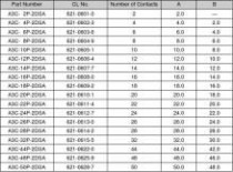
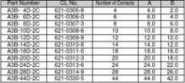
sPin Header
B


PCB mounting pattern

Note: Please order the product per 100 pcs.
Unit: mm
C15

元器件交易网www.61k.com
sReceptacle
qA3 Right Angle Type
BPCB mounting pattern
Unit: mm


Note: Please order the product per 100 pcs.
C16

元器件交易网www.61k.com
KA3C Type
B


PCB mounting pattern
Unit: mm
C17

元器件交易网www.61k.com
qA3D Type
B


PCB mounting pattern
Unit: mm
C18

元器件交易网www.61k.com
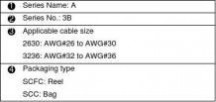
sCrimping SocketqA3B-*D-2C

Note 1. *indicates the number of contacts.Note 2. Please order the product per 100 pcs.Note 3. Use other contacts in combination.(Example: 50 contacts = 44 contacts + 6 contacts)qA4B-*S-2C


Note 1. *indicates the number of contacts.Note 2. Please, order the product per 100 pcs.
C19

元器件交易网www.61k.com
sCrimping Contact
SCC contact
SCFC contact
Note 1. The plating specification is shown as follows:
(Contact area) : Gold plating(Others): Nickel plating
Note 2. "30" is stamped on A3B-2630SCFC(SCC),
and "36" is stamped on A3B-3236SCFC(SCC).
BCrimping Tool
Manual crimping toolA3B-TA2630HC
Automatic crimping machineCM-105

C20

元器件交易网www.61k.com
B


Short Pin
Please, order the product per 1000 pcs.


BPolarizing Key
A3-GPIN(A)
Note: This product is provided in a set of 10 pieces in conjunction with a runner.
The unit for sale consists of 10 sets, which are included in one pack.
C21

元器件交易网www.61k.com
sPin Header
B


PCB mounting pattern
PCB mounting pattern for 4 pos.
Unit: mm
C22

元器件交易网www.61k.com
sReceptacle
B


PCB mounting pattern
PCB mounting pattern for 4 pos.
Unit: mm
C23

元器件交易网www.61k.com
BRecommended Temperature Profile

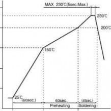
emperature (?)
Applicable
Reflow method
:IRreflow
:Paste type 63 Sn/37 Pb
(Flux content 9%/wt)
:Glass epoxy 85∞60∞1.6mm
SolderTest board
Metal mask thichness:0.2mm
Recommended temperature profile
The temperature may be slightly changed according to thesolder paste type and amount.
Time (Secounds)
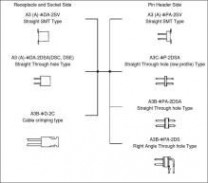
BFunctional Block Chart
C24

元器件交易网www.61k.com
BApplication Pattern (A3 series)
A3(A)-

*

DA-2SV

A3C-

*

DA-2DSA

A3B-

*

D-2C

A3(A)-

*

PA-2SV

A3C-*DA-2DSAA3(A)-*PA-2SVA3B-*D-2CA3(A)-*PA-2SVA3(A)-*DA-2SVA3C-*P-2DSA
A3(A)-*DA-2SVA3C-*P-2DSAA3C-*DA-2DSAA3C-*P-2DSAA3B-*D-2CA3B-*PA-2DSA
A3(A)-*DA-2SVA3B-*PA-2DSAA3C-*DA-2DSAA3B-*PA-2DSAA3B-*D-2CA3B-*PA-2DSA3B-*PA-2DSA3B-*PA-2DS
C25
二 : CA3310中文资料
元器件交易网www.cecb2b.com
CA3310, CA3310A
August 1997
CMOS, 10-Bit, A/D Converterswith Internal Track and Hold
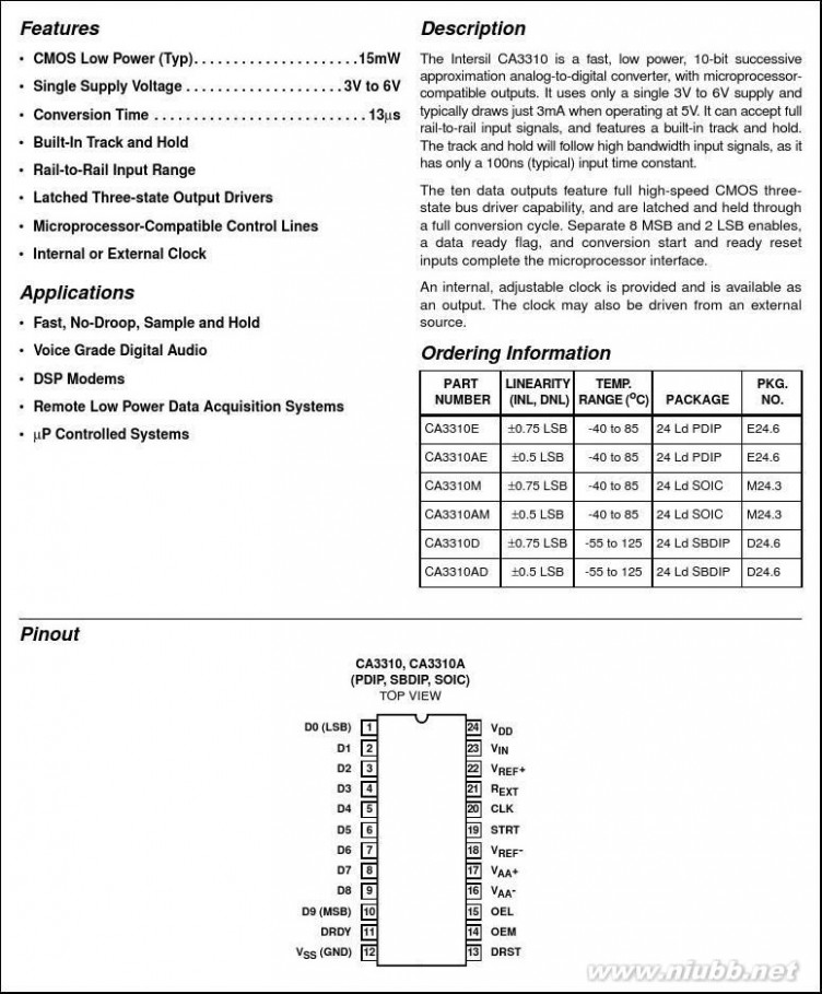
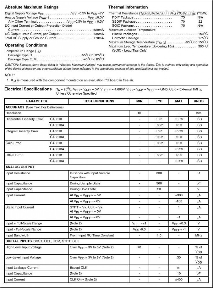
CAUTION: These devices are sensitive to electrostatic discharge; follow proper IC Handling Procedures.1-888-INTERSIL or 321-724-7143 | Copyright ? Intersil Corporation 1999
File Number
3095.1
6-6
ca3310 CA3310中文资料
元器件交易网www.cecb2b.com
CA3310, CA3310A
6-7

ca3310 CA3310中文资料
元器件交易网www.cecb2b.com
CA3310, CA3310A
6-8
ca3310 CA3310中文资料
元器件交易网www.cecb2b.com
CA3310, CA3310A
6-9
ca3310 CA3310中文资料
元器件交易网www.cecb2b.com
CA3310, CA3310A
6-10
ca3310 CA3310中文资料
元器件交易网www.cecb2b.com
CA3310, CA3310A
6-11
ca3310 CA3310中文资料
元器件交易网www.cecb2b.com
CA3310, CA3310A
6-12

ca3310 CA3310中文资料
元器件交易网www.cecb2b.com
CA3310, CA3310A
6-13
ca3310 CA3310中文资料
元器件交易网www.cecb2b.com
CA3310, CA3310A
6-14

ca3310 CA3310中文资料
元器件交易网www.cecb2b.com
CA3310, CA3310A
6-15
ca3310 CA3310中文资料
元器件交易网www.cecb2b.com
CA3310, CA3310A
6-16
ca3310 CA3310中文资料
元器件交易网www.cecb2b.com
CA3310, CA3310A
6-17

ca3310 CA3310中文资料
元器件交易网www.cecb2b.com
CA3310, CA3310A
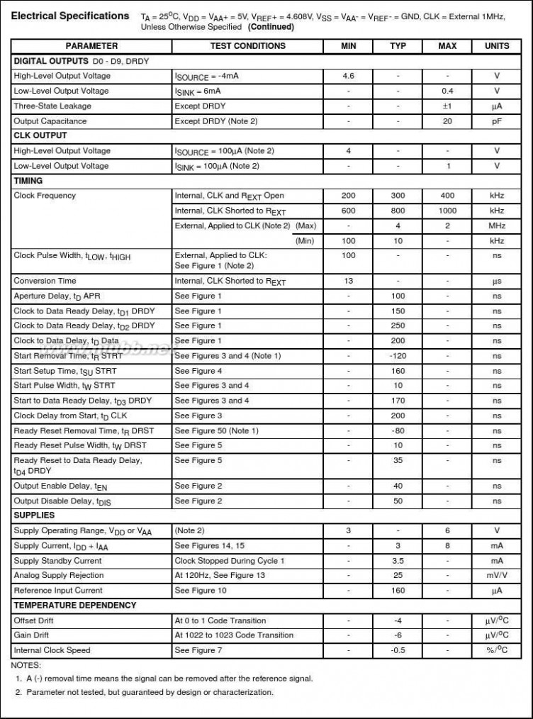
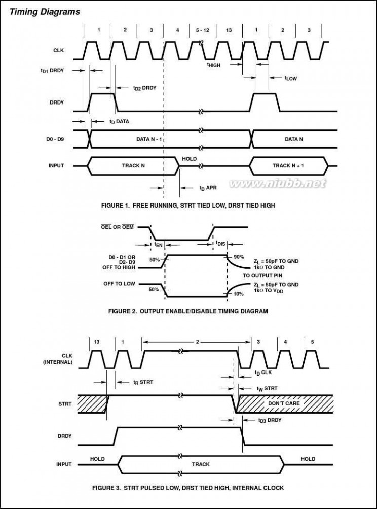
Other Accuracy Effects
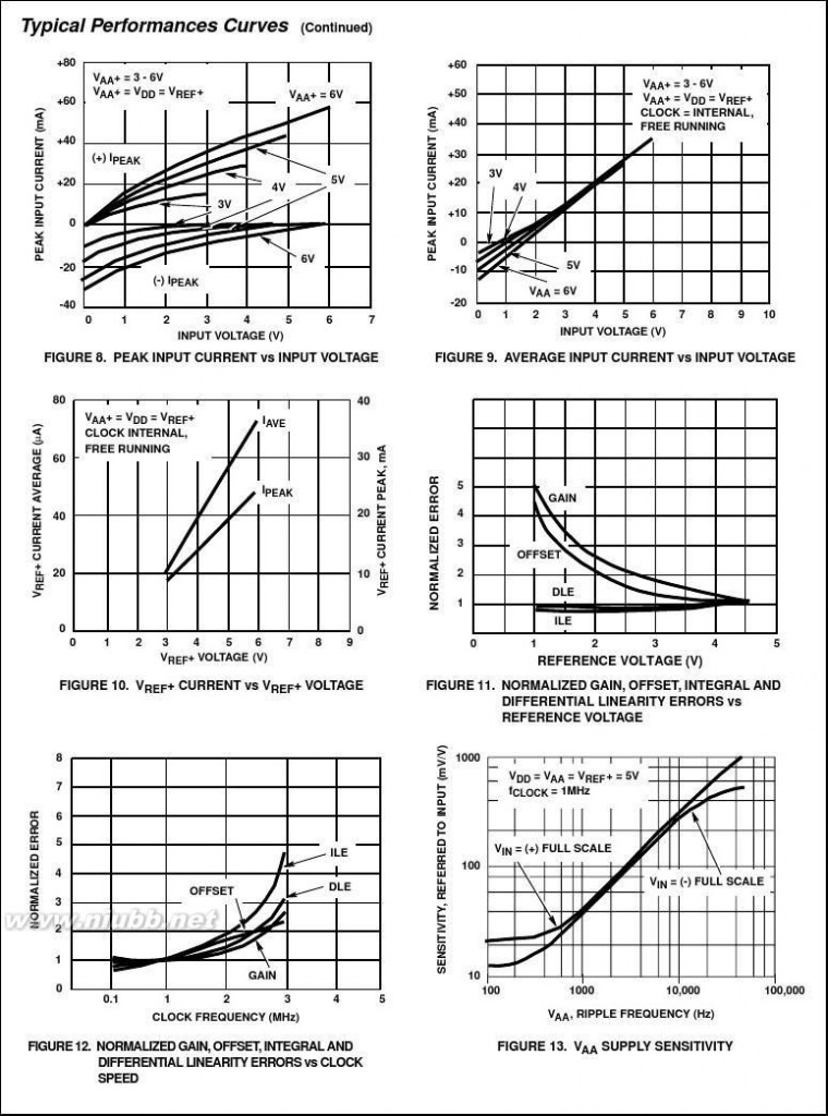
Linearity, offset, and gain errors are dependent on themagnitude of the full-scale input range, VREF+ - VREF-.Figure 11 shows how these errors vary with full-scale range.The clocking speed is a second factor that affects conversionaccuracy. Figure 12 shows the typical variation of linearity,offset, and gain errors versus clocking speed.
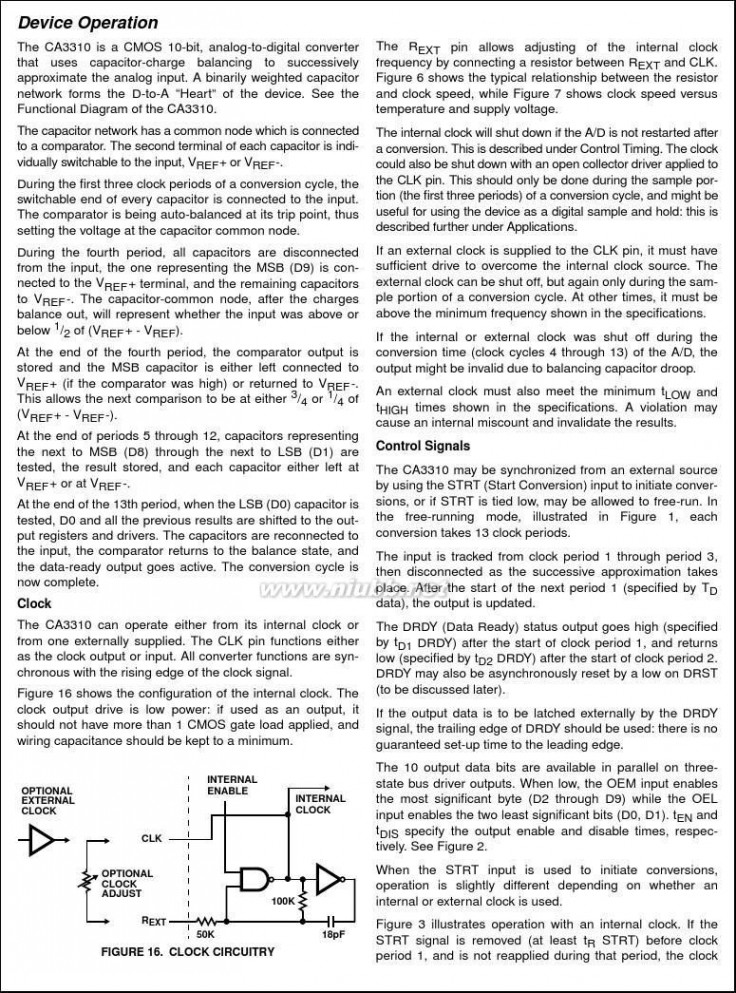
Gain and offset drift due to temperature are kept very low bymeans of auto-balancing the comparator. The speci?cationsshow typical offset and gain dependency on temperature.There is also very little linearity change with temperature, onlythat caused by the slight slowing of CMOS with increasingtemperature. At 85oC, for instance, the lLE and DLE would betypically those for a 20% faster clock than at 25oC.Power Supplies and Grounding
VDD(+) and VSS(GND) are the digital supply pins: theyoperate all internal logic and the output drivers. Because theoutput drivers can cause fast current spikes in the VDD andVSS lines, VSS should have a low impedance path to digitalground and VDD should be well bypassed.
Except for VDD+, which is a substrate connection to VDD, allpins have protection diodes connected to VDD and VSS:input transients above VDD or below VSS will get steered tothe digital supplies. Current on these pins must be limited byexternal means to the values speci?ed under maximumratings.
The VAA+ and VAA- terminals supply the charge-balancingcomparator only. Because the comparator is autobalancedbetween conversions, it has good low frequency supplyrejection. It does not reject well at high frequencies, how-ever: VAA- should be returned to a clean analog ground, andVAA+ should be RC decoupled from the digital supply.There is approximately 50? of substrate impedancebetween VDD and VAA+. This can be used, for example, aspart of a low-pass RC ?lter to attenuate switching supplynoise. A 10pF capacitor from VAA+ to ground wouldattenuate 30kHz noise by approximately 40dB. Note thatback-to-back diodes should be placed from VDD to VAA+ tohandle supply to capacitor turn-on or turn-off currentspikes.
Figure 16 shows VAA+ supply rejection versus frequency.Note that the frequency to be rejected scales with the clock:the 100Hz rejection with a 100kHz clock would be roughlyequivalent to the 1kHz rejection with a 1MHz clock.
扩展:ca3140中文资料 / smbj5.0ca中文资料 / smbj15ca中文资料
The supply current for the CA3310 is dependent on clockfrequency, supply voltage, and temperature. Figure 14shows the typical current versus frequency and voltage,while Figure 15 shows it versus temperature and voltage.Note that if stopped in auto-balance, the supply current istypicallysomewhat higher than if free-running. SeeSpeci?cations.
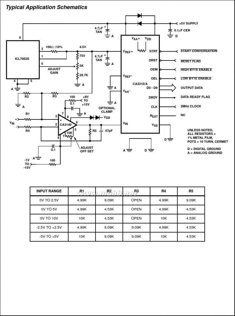
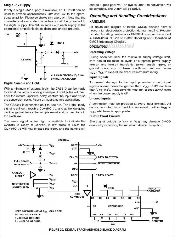
Application Circuits
Differential Input A/D System
As the CA3310 accepts a unipolar positive-analog input, theaccommodation of other ranges requires additional circuitry.The input capacitance and the input energy also force usinga low-impedance source for all but slow speed use. Figure20 shows the CA3310 with a reference, input ampli?er, andinput-scaling resistors for several input ranges.
The ICL7663S regulator was chosen as the reference, as itcan deliver less than 0.25V input-to-output (dropout) voltageand uses very little power. As high a reference as possible isgenerally desirable, resulting in the best linearity andrejection of noise at the CA3310.
The tantalum capacitor sources the VREF current spikesduring a conversion cycle. This relieves the response andpeak current requirements of the reference.
The CA3140 operational ampli?er provides good slewingcapability for high bandwidth input signals and can quicklysettle the energy that the CA3310 outputs at its VlN terminal.It can also drive close to the negative supply rail.
If system supply sequencing or an unknown input voltage islikely to cause the operational ampli?er to drive above theVDDsupply, a diode clamp can be added from pin 8 of theoperational ampli?er to the VDD supply. The minus drivecurrent is low enough not to require protection.
With a 2MHz clock (~150kHz sampling), Nyquist criteria wouldgive a maximum input bandwidth of 75kHz. The resistor valueschosen are low enough to not seriously degrade system band-width (an operational ampli?er settling) at that clock frequency.If A/D clock frequency and bandwidth requirements are lower,the resistor values (and input impedance) can be madecorrespondingly higher.
The A/D system would generally be calibrated by tying VlN- toground and applying a voltage to VIN+ that is 0.5 LSB (1/2048of full-scale range) above ground. The operational ampli?eroffset should be adjusted for an output code dithering between00016 and 00116 for unipolar use, or 10016 and 10116 for bipo-lar use. The gain would then be adjusted by applying a voltagethat is 1.5 LSB below the positive full scaleinput, and adjustingthe reference for an output dithering between 3FE16 and3FF16.
Note that R1 through R5 should be very well matched, asthey affect the common-mode rejection of the A/D system.Also, if R2 and R3 are not matched, the offset adjust of theoperational ampli?er may not have enough adjustment rangein bipolar systems.
The common-mode input range of the system is set by thesupply voltage available to the operational ampli?er. Therange that can be applied to the VIN- terminal can becalculated by:
?R4-------+1??R5??R4-------+1??R5?
VIN- for the most negative,
(VIN+ -2.5V) - (-------)VREF+ for the most positive.
R5
R4
6-18
ca3310 CA3310中文资料
元器件交易网www.cecb2b.com
CA3310, CA3310A
6-19
ca3310 CA3310中文资料
元器件交易网www.cecb2b.com
CA3310, CA3310A
6-20

扩展:ca3140中文资料 / smbj5.0ca中文资料 / smbj15ca中文资料
三 : LA3161中文资料
元器件交易网www.cecb2b.com
3161 LA3161中文资料
元器件交易网www.cecb2b.com
3161 LA3161中文资料
元器件交易网www.cecb2b.com
3161 LA3161中文资料
元器件交易网www.cecb2b.com
3161 LA3161中文资料
元器件交易网www.cecb2b.com
3161 LA3161中文资料
元器件交易网www.cecb2b.com
3161 LA3161中文资料
元器件交易网www.cecb2b.com
扩展:la3161 / tl431中文资料 / ds18b20中文资料
本文标题:中文资料-A4B-15PA-2DS中文资料61阅读| 精彩专题| 最新文章| 热门文章| 苏ICP备13036349号-1