一 : SGM9123中文资料
元器件交易网www.61k.com
Triple, 8MHz, 3rd Order

SDTV Video Filter Drivers
SG Microelectronics Co, Ltd Tel: 86/10/51798160/80 www.sg-micro.com
REV. A
元器件交易网www.61k.com
ELECTRICAL CHARACTERISTICS: VS = +5.0V
(At RL = 150Ω connected to GND, VIN = 1Vpp,and CIN = 0.1μF, all outputs AC coupled with 220μF,unless otherwise noted)
SGM9123
TYP MIN/MAX OVER TEMPERATURE
0℃ -40℃ MIN/
+25℃+25℃to+70℃ to+85℃ UNITSMAX
INPUT CHARACTERISTICS Output Level Shift Voltage (VOLS) Input Voltage Clamp (VCLAMP) Clamp Charge Current Voltage Gain ( AV)
VIN = 0V, no load IIN = -1mA
VIN = VCLAMP -100mV RL = 150?
VIN = 3V, RL = 150? to GND VIN = 3V, to GND through 10?
VIN = 100mV, out short to VDD through 10?
Vs = +2.7V to + 5.5V VIN = 500mV, RL = 150? RL = 150?
20% to 80%, VIN = 1V Step, NTSC & PAL DC coupled NTSC & PAL AC coupled NTSC & PAL DC coupled NTSC & PAL AC coupled f = 400KHz, 6.5MHz at 1MHz
2.0VSTEP, 80% to 20% 2.0VSTEP, 80% to 20%
258 -13 -5.60 2.0 4.42 110 162 66 7.4 5.4 8.0 +0.2 -25 44 0.2 0.52 0.4 1.0 17.5 -64 36
419-27-8.21.892.074.1568 1022.55.551 9.5
423 -27.6 -8.23 1.88 2.08 4.13 65 92 2.7 5.5 48 10.5
440 -28.7 -8.24 1.87 2.09 4.12 63 90 2.7 5.5 46 10.7
mVmVmAV/VV/VV mAmAV V dB mAMHz MHz dB dB V/μs% % ° ° ns dB ns
ns
MAX MIN MIN MIN MAX MIN MIN MINMIN MAX MIN MAX TYP TYP TYPTYPTYPTYPTYPTYPTYPTYPTYPTYPTYP
OUTPUT CHARACTERISTICS Output Voltage High Swing Output Short-Circuit Current (ISC)
POWER SUPPLY Operating Voltage Range
Power Supply Rejection Ratio (PSRR) Quiescent Current (IQ) DYNAMIC PERFORMANCE ±0.1dB Bandwidth -3dB Bandwidth Filter Response
Normalized Gain: fIN = 4.5MHz fIN = 27MHz Slew Rate
Differential Gain (DG)
Differential Phase (DP)
Group Delay Variation (D/DT) Crosstalk (channel - to - channel) Fall Time Rise Time
Specifications subject to change without notice.
2
SGM9123
元器件交易网www.61k.com
PACKAGE/ORDERING INFORMATION
ORDER NUMBER
PACKAGE TEMPERATUREDESCRIPTION RANGE
-40℃ to +125℃ PACKAGE OPTION
Tape and Reel, 2500 MARKING


INFORMATIONSGM9123XS

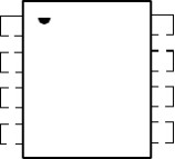
PIN CONFIGURATION

(Top View)


ABSOLUTE MAXIMUM RATINGS
Supply Voltage, V+ to V- .......................................... 6.5V Input Voltage
.......................... GND – 0.3 V to (+VS) +0.3V
Storage Temperature Range..................–65℃ to +150℃ Junction Temperature ............................................. 160℃ Operating Temperature Range ........... –40℃ to +125℃ Power Dissipation, PD @ TA = 25℃
SO-8 .............................................................................0.8W Package Thermal Resistance
SO-8, θJA................................................................ 125℃/W Lead Temperature Range (Soldering 10sec)
...................................................... 260℃
ESD Susceptibility
HBM...........................................................................8000V MM...............................................................................400V
NOTES
1. Stresses above those listed under Absolute Maximum Ratings may cause permanent damage to the device. This is a stress rating only; functional operation of the device at these or any other conditions above those indicated in the operational section of this specification is not implied. Exposure to absolute maximum rating conditions for extended periods may affect device reliability.
3
PIN DESCRIPTION
PIN
NAME
FUNCTION
Video input, channel 1 Video input, channel 2 Video input, channel 3 S
Power supply Ground Filtered output, channel 3Filtered output, channel 2Filtered output, channel 1
CAUTION
This integrated circuit can be damaged by ESD if you don’t pay attention to ESD protection. SG Micro-electronics recommends that all integrated circuits be handled with appropriate precautions. Failure to observe proper handling and installation procedures can cause damage.
ESD damage can range from subtle performance degradation to complete device failure. Precision integrated circuits may be more susceptible to damage because very small parametric changes could cause the device not to meet its published specifications.
SGM9123
元器件交易网www.61k.com
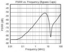
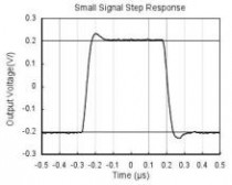
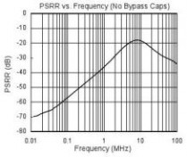
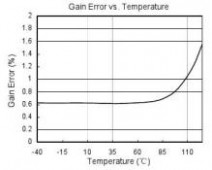
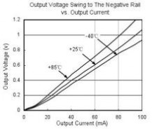
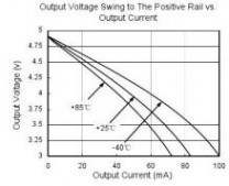
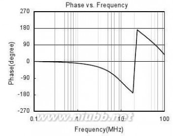
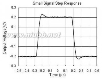
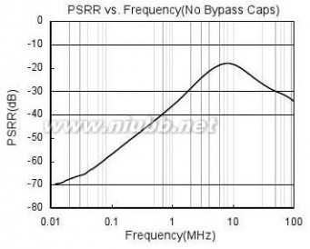
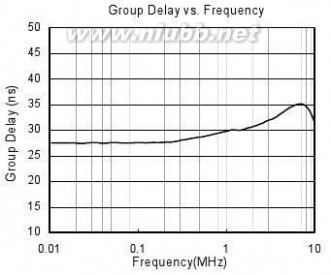
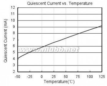
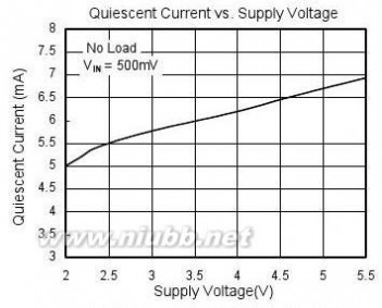
TYPICAL PERFORMANCE CHARACTERISTICS
At VS = +5.0V, TA = +25℃, RL = 150?, all outputs AC coupled with 220μF, unless otherwise noted.

4
SGM9123

元器件交易网www.61k.com
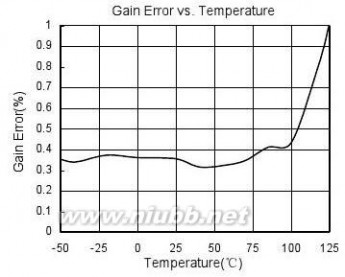
TYPICAL PERFORMANCE CHARACTERISTICS
At VS = +5.0V, TA = +25℃, RL = 150?, all outputs AC coupled with 220μF, unless otherwise noted.


5
SGM9123

元器件交易网www.61k.com
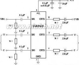
Applications Information
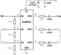
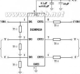
Typical Application Diagram
Functional Description
SGM9123 operates from a single +2.5V to +5V supply. In application, SGM9123 is a fully integrated solution for filtering and buffering SDTV signals in front of video decoder or behind video encoder. For example, SGM9123 can replace three passive LC filters and three amplifier drivers at CVBS and S-video output side in set-top box and DVD player, this solution can help you save PCB size and production cost, it also improves video signal performance comparing with traditional design using discrete components. SGM9123 features a DC-coupled input buffer, 3-pole low-pass filter to eliminate out-of-band noise of video encoder, and a gain of +6dB in the output amplifier to drive 75? load. The AC or DC-coupled input buffer eliminates sync crush, droop, and field tilt. The output of SGM9123 also can be DC-coupled or AC-coupled.
The following schematic in Figure 3 is normally used for AC coupled output and DC-coupled input with DAC which has an output voltage range of 0V to 1.4V. AC coupled output offer slightly lower power dissipation and high ESD protection ability. The schematics in Figure 1 and Figure 2 are also popular in design. Figure 4 is a kind of special application in STB.


S-Video
Input Considerations
Besides AC coupling, the SGM9123 inputs also can be DC-coupled. In DC coupling application, No input coupling capacitors are needed because the amplitude of input video signal from DAC includes ground and extends up to 1.4V, then SGM9123 can be directly connected to the output of a single-supply, current-output DAC without any external bias network. Some time, if DAC’s output level exceeds the range of 0V to 1.4V, or SGM9123 is driven by an unknown external source or a SCART switch which has its own clamping circuit, AC coupling is needed in such applications.
Figure 1. DC Coupling Application Schematic


Output Considerations
The SGM9123 outputs can be DC-coupled or AC-coupled. When 0V is input, the SGM9123 output voltage is 260mV typically. In DC coupling design, one 75? resistor is used to Connect SGM9123’s output pin with external load directly, this serial back-termination resistor is used to match the impedance of the transmission line between SGM9123 and external load to cancel the signal reflection. The SGM9123 outputs can sink and source current allowing the device to be AC-coupled with external load, in AC coupling, 220μF at least capacitor will be used in order to eliminate field tilt.
Figure 2. AC Coupling Application Schematic
1
Power-Supply Bypassing and Layout
Correct power supply bypassing is very important for optimizing video performance in design. One 0.1μF and one 10μF capacitors are always used to Bypass VCC pin of SGM9123, please place these two capacitors as close to the SGM9123 output pin as possible, a large ground plane is also needed to ensure optimum performance. The input and output termination resistors should be placed as close to the related pin of SGM9123 as possible to avoid performance degradation. The PCB traces at the output side should have 75? characteristic impedance in order to match the 75? characteristic impedance cable connecting external load. In design, please keep the board trace at the inputs and outputs of the SGM9123 as short as possible to minimize the parasitic stray capacitance and noise pickup.
S-Video
Coupling Application Schematic
6
SGM9123
元器件交易网www.61k.com
Figure 4. Input DC Coupling and Output AC Coupling Application Schematic in STB
7 SGM9123


元器件交易网www.61k.com
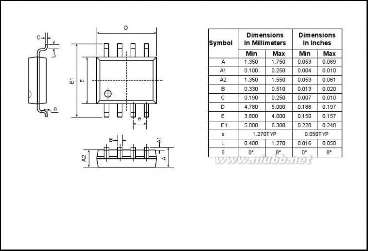
PACKAGE OUTLINE DIMENSIONS
SO-8

8
SGM9123
元器件交易网www.61k.com
REVISION HISTORY
Location Page 11/2007— Preliminary Data Sheet
01/2008— Data Sheet REV.A
SG Microelectronics Co., Ltd
A2608, NO.72 North Road
Xisanhuan, Haidian District,
Beijing, China 100037
Tel: 86-10-51798160/80
Fax: 86-10-51798180-803
9 SGM9123
二 : SGM9115ZS中文资料
元器件交易网www.cecb2b.com
SGM9115
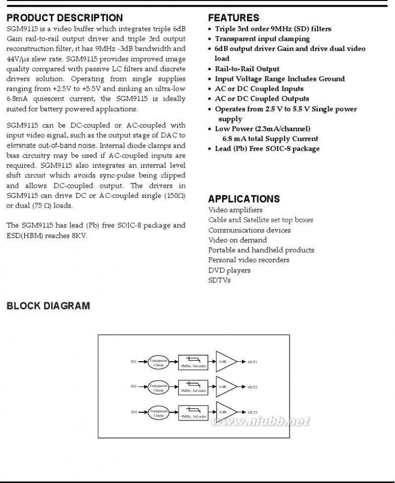
Triple, 9MHz, 3rd Order SDTV Video Filter Drivers
Shengbang Microelectronics Co, Ltd Tel: 86/451/84348461 www.sg-micro.com
REV. B
9115 SGM9115ZS中文资料
元器件交易网www.cecb2b.com
ELECTRICAL CHARACTERISTICS: VS = +5.0V
(At RL = 150Ω connected to GND, Vin=1Vpp,and CIN = 0.1μF, all outputs AC coupled with 220μF,unless otherwise noted)
SGM9115
TYP
+25℃
INPUT CHARACTERISTICS Output Level Shift Voltage (VOLS) Input Bias Current (IB) Input Voltage Clamp (VCLAMP) Clamp Charge Current Input Resistance (RIN) Voltage Gain ( AV)
VIN = 0V, no load
IIN = -1mA
VIN = VCLAMP -100mV 0.5V < VIN < 1.0V RL = 150?
VIN = 3V, RL = 150? to GND VIN = 3V, to GND through 10?
VIN = 100mV, out short to VDD through 10?
Vs = +2.7 V to + 5.5 V VIN = 500mV, RL = 150? RL = 150?
20% to 80%, VIN = 1V Step, NTSC & PAL DC coupled NTSC & PAL AC coupled NTSC & PAL DC coupled NTSC & PAL AC coupled f = 400KHz, 6.5MHz at 1MHz
2.0VSTEP, 80% to 20% 2.0VSTEP, 80% to 20%
258 -15 -5 2.0 4.4 -104 110 60 6.8 4.5 9.0 -0.1 -22 44 0.2 0.52 0.4 1.0 5.5 -64 36 38
340 -20-5.9 1.952.044.3-1001032.55.558 7.8
350 -21 -6 1.93 2.06 4.29 2.7 5.5 58 8.0
380 -24 -6.5 1.91 2.08 4.25 2.7 5.5 57 8.5
400 -27 -7 1.90 2.09 4.2 2.7 5.5 56 9.0
mVpA mVmAM?V/VV/VV mAmAV V dB mAMHz MHz dB dB V/μs% % ° ° ns dB ns ns
MAX TYPMIN MIN MIN MIN MAX MINMAX MINMIN MAX MIN MAX TYP TYP TYPTYPTYPTYPTYPTYPTYPTYPTYPTYPTYP
MIN/MAX OVER TEMPERATURE 0℃ -40℃
to70℃ to 85℃
-40℃ MIN/to 125℃UNITSMAX
+25℃
OUTPUT CHARACTERISTICS Output Voltage High Swing Output Short-Circuit Current (ISC)
POWER SUPPLY Operating Voltage Range
Power Supply Rejection Ratio (PSRR)Quiescent Current (IQ) DYNAMIC PERFORMANCE ±0.1dB Bandwidth -3dB Bandwidth Filter Response
Normalized Gain: fIN = 4.5MHz fIN = 27MHz Slew Rate
Differential Gain (DG)
Differential Phase (DP)
Group Delay Variation (D/DT) Crosstalk (channel - to - channel) Fall Time Rise Time
Specifications subject to change without notice.
2
SGM9115
9115 SGM9115ZS中文资料
元器件交易网www.cecb2b.com
PACKAGE/ORDERING INFORMATION
ORDER NUMBER
PACKAGE DESCRIPTION
TEMPERATURE
RANGE
PACKAGE OPTION
MARKING INFORMATION
0℃ to +70℃ -40℃ to +125℃
Tape and Reel, 2500 Tape and Reel, 2500
SGM9115ZS SGM9115XS
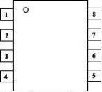
PIN CONFIGURATIONS (Top View)
SGM9115
IN1OUT1IN2OUT2IN3OUT3+VS
GND
SO-8
ABSOLUTE MAXIMUM RATINGS
Supply Voltage, V+ to V- ......................................... 7.5 V Input Voltage
.......................... GND – 0.3 V to (+VS) +0.3V
Storage Temperature Range..............–65℃ to +150℃ Junction Temperature ............................................. 160℃ Operating Temperature Range ........... –40℃ to +125℃ Power Dissipation, PD @ TA = 25℃
SO-8 .............................................................................0.8W Package Thermal Resistance
SO-8, θJA................................................................ 128℃/W Lead Temperature Range (Soldering 10 sec)
...................................................... 260℃
ESD Susceptibility
HBM...........................................................................8000V MM...............................................................................400V
NOTES
1. Stresses above those listed under Absolute Maximum Ratings may cause permanent damage to the device. This is a stress rating only; functional operation of the device at these or any other conditions above those indicated in the operational section of this specification is not implied. Exposure to absolute maximum rating conditions for extended periods may affect device reliability.
3
PIN DESCRIPTION
PIN
NAME
FUNCTION
Video input, channel 1 Video input, channel 2 Video input, channel 3 S
Power supply Ground Filtered output, channel 3 Filtered output, channel 2 Filtered output, channel 1
CAUTION
This integrated circuit can be damaged by ESD if you don’t pay attention to ESD protection. Shengbang Micro-electronics recommends that all integrated circuits be handled with appropriate precautions. Failure to observe proper handling and installation procedures can cause damage.
ESD damage can range from subtle performance degradation to complete device failure. Precision integrated circuits may be more susceptible to damage because very small parametric changes could cause the device not to meet its published specifications.
扩展:sgm3157中文资料 / sgm7227中文资料 / sgm4056中文资料
SGM9115
9115 SGM9115ZS中文资料
元器件交易网www.cecb2b.com
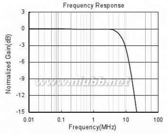
TYPICAL PERFORMANCE CHARACTERISTICS
At VS = +5.0V, TA = +25℃, RL = 150?, all outputs AC coupled with 220μF, unless otherwise noted.


4
SGM9115
9115 SGM9115ZS中文资料
元器件交易网www.cecb2b.com
TYPICAL PERFORMANCE CHARACTERISTICS
At VS = +5.0V, TA = +25℃, RL = 150?, all outputs AC coupled with 220μF, unless otherwise noted.


5
SGM9115
9115 SGM9115ZS中文资料
元器件交易网www.cecb2b.com
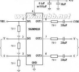
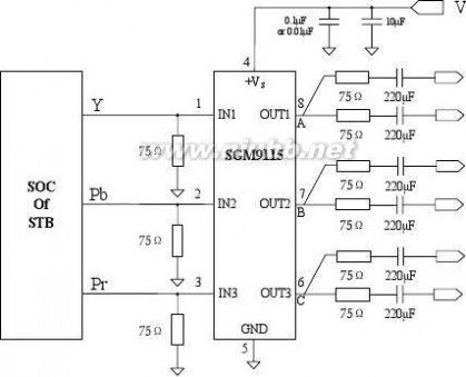
Applications Information
Functional Description
Typical Application Diagram
SGM9115 operates from a single +2.5V to +5V supply. In application, SGM9115 is a fully integrated solution for filtering and buffering SDTV signals in front of video decoder or behind video encoder. For example, SGM9115 can replace three passive LC filters and three amplifier drivers at CVBS and S-video output side in set-top box and DVD player, this solution can help you save PCB size and production cost, it also improves video signal performance comparing with traditional design using discrete components. SGM9115 features a DC-coupled input buffer, 3-pole low-pass filter to eliminate out-of-band noise of video encoder, and a gain of +6dB in the output amplifier to drive 75? load. The AC or DC-coupled input buffer eliminates sync crush, droop, and field tilt. The output of SGM9115 also can be DC-coupled or AC-coupled.
The following schematic in Figure 3 is normally used for AC coupled output and DC-coupled input with DAC which has an output voltage range of 0V to 1.4V. AC coupled output offer slightly lower power dissipation and high ESD protection ability. The schematics in Figure 1 and Figure 2 are also popular in design. Figure 4 is a kind of special application in STB.
S-Video
Input Considerations
Besides AC coupling, the SGM9115 inputs also can be DC-coupled. In DC coupling application, No input coupling capacitors are needed because the amplitude of input video signal from DAC includes ground and extends up to 1.4V, then SGM9115 can be directly connected to the output of a single-supply, current-output DAC without any external bias network. Some time, if DAC’s output level exceeds the range of 0V to 1.4V, or SGM9115 is driven by an unknown external source or a SCART switch which has its own clamping circuit, AC coupling is needed in such applications.
Figure 1. DC Coupling Application Schematic
S-Video
1
Output Considerations
The SGM9115 outputs can be DC-coupled or AC-coupled. When 0V is input, the SGM9115 output voltage is 260mV typically. In DC coupling design, one 75? resistor is used to Connect SGM9115’s output pin with external load directly, this serial back-termination resistor is used to match the impedance of the transmission line between SGM9115 and external load to cancel the signal reflection. The SGM9115 outputs can sink and source current allowing the device to be AC-coupled with external load, in AC coupling, 220μF at least capacitor will be used in order to eliminate field tilt.
S-Video
Power-Supply Bypassing and Layout
Figure 2. AC Coupling Application Schematic
1
Correct power supply bypassing is very important for optimizing video performance in design. One 0.1μF and one 10μF capacitors are always used to Bypass VCC pin of SGM9115, please place these two capacitors as close to the SGM9115 output pin as possible, a large ground plane is also needed to ensure optimum performance. The input and output termination resistors should be placed as close to the related pin of SGM9115 as possible to avoid performance degradation. The PCB traces at the output side should have 75? characteristic impedance in order to match the 75? characteristic impedance cable connecting external load. In design, please keep the board trace at the inputs and outputs of the SGM9115 as short as possible to minimize the parasitic stray capacitance and noise pickup.
扩展:sgm3157中文资料 / sgm7227中文资料 / sgm4056中文资料
S-Video
Coupling Application Schematic
6
SGM9115
9115 SGM9115ZS中文资料
元器件交易网www.cecb2b.com
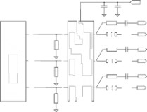
to Loading 1
to Loading 2
to Loading 1
to Loading 2
to Loading 1
to Loading 2
The three ports of A ,B and C should be immediate as signal output pin in layout
Figure 4. Input DC Coupling and Output AC Coupling Application Schematic in STB
7
SGM9115
9115 SGM9115ZS中文资料
元器件交易网www.cecb2b.com
PACKAGE OUTLINE DIMENSIONS
SO-8
8
SGM9115
9115 SGM9115ZS中文资料
元器件交易网www.cecb2b.com
REVISION HISTORY
Location Page 11/06— Data Sheet changed from preliminary to REV. A
Changes to ABSOLUTE MAXIMUM RATINGS . . . . . . . . . . . . . . . . . . . . . . . . . . . . . . . . . . . . . . . . . . . . . . . . . . . . . . . . . . . . . . . . . . . . . . . . 3
06/07— Data Sheet changed from REV. A to REV. B
Adds applications information . . . . . . . . . . . . . . . . . . . . . . . . . . . . . . . . . . . . . . . . . . . . . . . . . . . . . . . . . . . . . . . . . . . . . . . . . . . . . . . . . . . . . 7
Shengbang Microelectronics Co, Ltd
Unit 3, ChuangYe Plaza
No.5, TaiHu Northern Street, YingBin Road Centralized Industrial Park
Harbin Development Zone
Harbin, HeiLongJiang 150078
P.R. China
Tel.: 86-451-84348461
Fax: 86-451-84308461
9 SGM9115
扩展:sgm3157中文资料 / sgm7227中文资料 / sgm4056中文资料
三 : CA139_01中文资料
元器件交易网www.cecb2b.com
T
DUCEMENTORPC
ETEREPLALO
OBSENDEDOMMDataSheetREC
CA139,CA139A,CA239,CA339,
LM339,LM2901,LM3302
May2001
FileNumber
795.7
NO
QuadVoltageComparatorsforIndustrial,CommercialandMilitaryApplicationsFeatures
?OperationfromSingleorDualSupplies?CommonModeInputVoltageRangetoGND?OutputVoltageCompatiblewithTTL,DTL,ECL,MOSandCMOS?DifferentialInputVoltageRangeEqualtotheSupplyVoltage
?MaximumInputOffsetVoltage(VIO)
-CA139A.................................2mV-CA139,CA239,CA339......................5mV-LM2901..................................7mV-LM3302.................................20mV?ReplacementforIndustryTypes139,239,339,139A,2901,3302
Thedevicesinthisseriesconsistoffourindependentsingleordualsupplyvoltagecomparatorsonasinglemonolithicsubstrate.Thecommonmodeinputvoltagerangeincludesgroundevenwhenoperatedfromasinglesupply,andthelowpowersupplycurrentdrainmakesthesecomparatorssuitableforbatteryoperation.ThesetypesweredesignedtodirectlyinterfacewithTTLandCMOS.
TypeCA139A,hasalowerinputoffsetvoltagethantheCA139.SomeoftheSOICpartsareavailableontapeandreel(seeOrderingInformationtable).ReplacetheMsuffixinthepartnumberwithM96whenordering(e.g.,CA0239M96).
PartNumberInformation
Applications
?SquareWaveGenerator?TimeDelayGenerators?PulseGenerators?Multivibrators
?HighVoltageDigitalLogicGates?A/DConverters?MOSClockTimers
SchematicDiagram
V+3
TO2,3,4
3.5μA
100μA
3.5μA
100μA
Pinout
CA139A(SOIC)
CA139,CA339,LM3302(PDIP,SOIC)CA239,LM2901,LM339(PDIP)
TOPVIEW
+INPUT
5
Q1
Q2Q3
Q4
Q8
OUTPUT2
OUTPUT2OUTPUT1
V+
NEG.INPUT1POS.INPUT1NEG.INPUT2POS.INPUT2
1234567
14OUTPUT313OUTPUT412GND
11POS.INPUT410NEG.INPUT498
POS.INPUT3NEG.INPUT3
4
-INPUT
Q5Q6Q7
TO2,3,4
76
+
-
21
COMPARATORNO1
+-4
98
+
-
31

CAUTION:Thesedevicesaresensitivetoelectrostaticdischarge;followproperICHandlingProcedures.
1-888-INTERSILor321-724-7143|IntersilandDesignisatrademarkofIntersilAmericasInc.|Copyright?IntersilAmericasInc.2001
ca139 CA139_01中文资料
元器件交易网www.cecb2b.com
CA139,CA139A,CA239,CA339,LM339,LM2901,LM3302
AbsoluteMaximumRatings
SupplyVoltage................................36Vor±18VDifferentialInputVoltage...............................36VInputVoltage................................-0.3Vto+36VInputCurrent(VI<-0.3V,Note1)......................50mAOutputShortCircuitDuration(SingleSupply,Note2)...Continuous
ThermalInformation
ThermalResistance(Typical,Note3)
θJA(oC/W)
θJC(oC/W)
PDIPPackage...................100N/ASOICPackage...................175N/AMaximumJunctionTemperature(PlasticPackage).........150oCMaximumStorageTemperatureRange..........-65oCto150oCMaximumLeadTemperature(Soldering10s)............300oC(SOIC-LeadTipsOnly)
OperatingConditions
TemperatureRange
CA139,CA139A..........................-55oCto125oCCA239..................................-25oCto80oCCA339,LM339.............................0oCto70oCLM2901,LM3302..........................-40oCto85oC
CAUTION:Stressesabovethoselistedin“AbsoluteMaximumRatings”maycausepermanentdamagetothedevice.Thisisastressonlyratingandoperationofthedeviceattheseoranyotherconditionsabovethoseindicatedintheoperationalsectionsofthisspecificationisnotimplied.
NOTES:
1.Inputsmustnotgomorenegativethan-0.3V.
2.ShortcircuitsfromtheoutputtoV+cancauseexcessiveheatingandeventualdestruction.ThemaximumoutputcurrentindependentofV+isapproximately20mA.3.θJAismeasuredwiththecomponentmountedonanevaluationPCboardinfreeair.
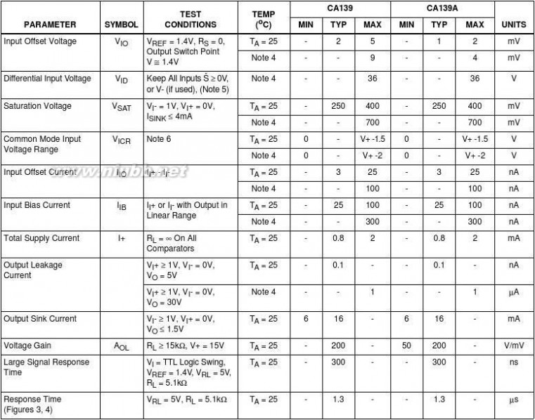
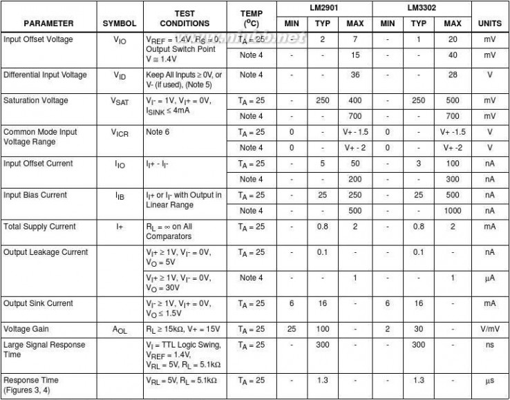
ElectricalSpecifications
V+=5V,UnlessOtherwiseSpecified
2
ca139 CA139_01中文资料
元器件交易网www.cecb2b.com
CA139,CA139A,CA239,CA339,LM339,LM2901,LM3302
ElectricalSpecifications
V+=5V,UnlessOtherwiseSpecified

NOTES:
4.AmbientTemperature(TA)applicableoveroperatingtemperaturerangeasshownbelow.
CA139,CA139A=-55oCto125oC;CA239=-25oCto85oC;CA339,LM339=0oCto70oC;LM2901,LM3302=-40oCto85oC.
5.Thecomparatorwillprovideaproperoutputstateevenifthepositiveswingoftheinputsexceedsthepowersupplyvoltagelevel,iftheotherinputremainswithinthecommonmodevoltagerange.Thelowinputvoltagestatemustnotbelessthan-0.3V(or0.3Vbelowthemagnitudeofthenegativepowersupply,ifused).6.Theupperendofthecommonmodevoltagerangeis(V+)-1.5V,buteitherorbothinputscangoto+30Vwithoutdamage.
扩展:6n139中文资料 / lm139中文资料 / bt139中文资料
3
ca139 CA139_01中文资料
元器件交易网www.cecb2b.com
CA139,CA139A,CA239,CA339,LM339,LM2901,LM3302
ElectricalSpecifications
V+=5V,UnlessOtherwiseSpecified
TypicalPerformanceCurves
RL=∞
1.0SUPPLYCURRENT(mA)
0.80.60.40.2
-55C0oC25C70C125C
INPUTCURRENT(nA)
VIC=0VRIC=109?
-55oC0oC25oC
302010
70oC125oC
605040
0102030
010203040
POSITIVESUPPLYVOLTAGE(V)POSITIVESUPPLYVOLTAGE(V)
FIGURE1.SUPPLYCURRENTvsSUPPLYVOLTAGEFIGURE2.INPUTCURRENTvsSUPPLYVOLTAGE
4
ca139 CA139_01中文资料
元器件交易网www.cecb2b.com
CA139,CA139A,CA239,CA339,LM339,LM2901,LM3302
TypicalPerformanceCurves
TA=25C
V+=+5VVI45
OUTPUTVOLTAGE(V)
543210
0.5
100mV
20mV
INPUT
OVERDRIVE=5mV1.0TIME(μs)
1.5
2.0
-3
INPUTVOLTAGE(mV)
0-50-100
5.1k?2VO
OUTPUTV

OLTAGE(V)
543210
0.5
100mV
20mV
INPUT
OVERDRIVE=5mVTA=25oC
500
V+=+5VVI45
-3
INPUTVOLTAGE(mV)100
5.1k?2
VO
1.0TIME(μs)
1.52.0
FIGURE3.RESPONSETIMEFORVARIOUSINPUT
OVERDRIVES-NEGATIVETRANSITION
101OUTPUTSATURATIONVOLTAGE(V)
TA=25C
FIGURE4.RESPONSETIMEFORVARIOUSINPUT
OVERDRIVES-POSITIVETRANSITION
OUTOFSATURATION
100
10-1
10-2
10-3
10-2
10-1100101102
OUTPUTSINKCURRENT(mA)
FIGURE5.OUTPUTSATURATIONVOLTAGEvsOUTPUTSINKCURRENT
MetallizationMaskLayout
05450
10
20
30
40
5055
40
30
(1
20
NOTE:Dimensionsinparenthesesareinmmandarederivedfromthebasicin.dimensionsasindicated.Gridgraduationsareinmils(10-3inch).
10
4-10(0.102-0.254)
52-60(1.321-1.524)
5
ca139 CA139_01中文资料
元器件交易网www.cecb2b.com
CA139,CA139A,CA239,CA339,LM339,LM2901,LM3302
AllIntersilproductsaremanufactured,assembledandtestedutilizingISO9000qualitysystems.
IntersilCorporation’squalitycertificationscanbeviewedatwebsiteIntersilproductsaresoldbydescriptiononly.IntersilCorporationreservestherighttomakechangesincircuitdesignand/orspecificationsatanytimewithoutnotice.Accordingly,thereaderiscautionedtoverifythatdatasheetsarecurrentbeforeplacingorders.InformationfurnishedbyIntersilisbelievedtobeaccurateandreliable.How-ever,noresponsibilityisassumedbyIntersiloritssubsidiariesforitsuse;norforanyinfringementsofpatentsorotherrightsofthirdpartieswhichmayresultfromitsuse.NolicenseisgrantedbyimplicationorotherwiseunderanypatentorpatentrightsofIntersiloritssubsidiaries.
ForinformationregardingIntersilCorporationanditsproducts,seewebsitewww.intersil.com
SalesOfficeHeadquarters
NORTHAMERICA
IntersilCorporation
2401PalmBayRd.
PalmBay,FL32905
TEL:(321)724-7000
FAX:(321)724-7240EUROPEIntersilSAMercureCenter100,RuedelaFusee1130Brussels,BelgiumTEL:(32)2.724.2111
FAX:(32)2.724.22.05ASIAIntersilLtd.8F-2,96,Sec.1,Chien-kuoNorth,Taipei,Taiwan104RepublicofChinaTEL:886-2-2515-8508FAX:886-2-2515-8369
6
扩展:6n139中文资料 / lm139中文资料 / bt139中文资料
本文标题:中文资料-SGM9123中文资料61阅读| 精彩专题| 最新文章| 热门文章| 苏ICP备13036349号-1