一 : SSTA中文资料
元器件交易网www.cecb2b.com
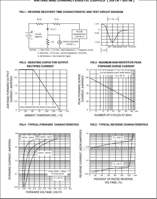
SSTA - SSTM
PRV : 50 - 1000 VoltsIo : 2.5 Amperes
FEATURES :
* High current capability
* High surge current capability * High reliability
* Low reverse current
* Low forward voltage drop * Super fast recovery time * Pb / RoHS Free
SURFACE MOUNT SUPER FAST RECTIFIERS
MECHANICAL DATA :
* Case : SMB Molded plastic
* Epoxy : UL94V-O rate flame retardant * Lead : Lead Formed for Surface Mount * Polarity : Color band denotes cathode end * Mounting position : Any * Weight : 0.1079 gram
MAXIMUM RATINGS AND ELECTRICAL CHARACTERISTICS
Rating at 25 °C ambient temperature unless otherwise specified.Single phase, half wave, 60 Hz, resistive or inductive load. For capacitive load, derate current by 20%.
RATING
Maximum Recurrent Peak Reverse Voltage Maximum RMS Voltage Maximum DC Blocking Voltage
Maximum Average Forward Current Ta = 55 °C Maximum Peak Forward Surge Current 8.3 ms. Single half sine wave Superimposed on rated load (JEDEC Method)
Maximum Peak Forward Voltage at IF = 2.5 A. Maximum DC Reverse Current Ta = 25 °C at Rated DC Blocking Voltage Ta = 100 °C Maximum Reverse Recovery Time ( Note 1 ) Typical Junction Capacitance ( Note 2 ) Junction Temperature Range Storage Temperature Range
SYMBOLSSTASSTBSSTCSSTDSSTESSTGSSTJSSTKSSTMUNIT
VRRMVRMSVDCIF(AV)IFSMVFIRIR(H)
Trr
503550
10070100
150105150
200140200
3002103002.5100
400280400
600420600
800560800
10007001000
VVVAA
0.95
5.0503550
1.72.5VμAμAnspf°C°C
CJTJTSTG
- 65 to + 150 - 65 to + 150
Notes :
( 1 ) Reverse Recovery Test Conditions : IF

= 0.5 A, I

R

= 1.0 A, Irr = 0.25 A. ( 2 ) Measured at 1.0 MHz and applied reverse voltage of 4.0 VDC
Page 1 of 2Rev. 04 : March 25, 2005
SSTA SSTA中文资料
元器件交易网www.cecb2b.com


Page 2 of 2Rev. 04 : March 25, 2005
二 : HFA3096BZ96中文资料
元器件交易网www.cecb2b.com
?
HFA3046, HFA3096, HFA3127, HFA3128
Data Sheet
December 21, 2005
FN3076.13
Ultra High Frequency Transistor Arrays
The HFA3046, HFA3096, HFA3127 and the HFA3128 are Ultra High Frequency Transistor Arrays that are fabricated from Intersil Corporation’s complementary bipolar UHF-1 process. Each array consists of five dielectrically isolated transistors on a common monolithic substrate. The NPN transistors exhibit a fT of 8GHz while the PNP transistors provide a fT of 5.5GHz. Both types exhibit low noise (3.5dB), making them ideal for high frequency amplifier and mixer applications.
The HFA3046 and HFA3127 are all NPN arrays while the HFA3128 has all PNP transistors. The HFA3096 is an NPN-PNP combination. Access is provided to each of the terminals for the individual transistors for maximum application flexibility. Monolithic construction of these transistor arrays provides close electrical and thermal matching of the five transistors.
Intersil provides an Application Note illustrating the use of these devices as RF amplifiers. For more information, visit our website at www.intersil.com.
Features
?NPN Transistor (fT) . . . . . . . . . . . . . . . . . . . . . . . . . 8GHz?NPN Current Gain (hFE). . . . . . . . . . . . . . . . . . . . . . . .130?NPN Early Voltage (VA) . . . . . . . . . . . . . . . . . . . . . . . 50V?PNP Transistor (fT). . . . . . . . . . . . . . . . . . . . . . . . .5.5GHz?PNP Current Gain (hFE). . . . . . . . . . . . . . . . . . . . . . . . .60?PNP Early Voltage (VA) . . . . . . . . . . . . . . . . . . . . . . . .20V?Noise Figure (50?) at 1.0GHz. . . . . . . . . . . . . . . . . 3.5dB?Collector to Collector Leakage. . . . . . . . . . . . . . . . . .<1pA ?Complete Isolation Between Transistors
?Pin Compatible with Industry Standard 3XXX Series
Arrays?Pb-Free Plus Anneal Available (RoHS Compliant)
Applications
?VHF/UHF Amplifiers?VHF/UHFMixers?IF Converters
?Synchronous Detectors
Ordering Information
PART NUMBER*HFA3046BHFA3046BZ (Note)HFA3096BHFA3096BZ (Note)HFA3127BHFA3127BZ (Note)HFA3127RHFA3127RZ (Note)HFA3128BHFA3128BZ (Note)HFA3128RHFA3128RZ (Note)
PART MARKINGHFA3046BHFA3046BZHFA3096BHFA3096BZHFA3127BHFA3127BZ127127ZHFA3128BHFA3128BZ128128Z
TEMP. RANGE (°C)
-55 to 125-55 to 125-55 to 125-55 to 125-55 to 125-55 to 125-55 to 125-55 to 125-55 to 125-55 to 125-55 to 125-55 to 125
PACKAGE
14 Ld SOIC
14 Ld SOIC (Pb-free)16 Ld SOIC
16 Ld SOIC (Pb-free)16 Ld SOIC
16 Ld SOIC (Pb-free)16 Ld 3x3 QFN
16 Ld 3x3 QFN (Pb-free)16 Ld SOIC
16 Ld SOIC (Pb-free)16 Ld 3x3 QFN
16 Ld 3x3 QFN (Pb-free)
PKG. DWG. #M14.15M14.15M16.15M16.15M16.15M16.15L16.3x3L16.3x3M16.15M16.15L16.3x3L16.3x3
*Add “96” suffix for tape and reel.
NOTE:Intersil Pb-free plus anneal products employ special Pb-free material sets; molding compounds/die attach materials and 100% matte tin plate termination finish, which are RoHS compliant and compatible with both SnPb and Pb-free soldering operations. Intersil Pb-free products are MSL classified at Pb-free peak reflow temperatures that meet or exceed the Pb-free requirements of IPC/JEDEC J STD-020.
1
CAUTION: These devices are sensitive to electrostatic discharge; follow proper IC Handling Procedures.1-888-INTERSIL or 1-888-468-3774|Intersil (and design) is a registered trademark of Intersil Americas Inc.
Copyright Intersil Americas Inc. 1998, 2005. All Rights Reserved
All other trademarks mentioned are the property of their respective owners.
HFA HFA3096BZ96中文资料
元器件交易网www.cecb2b.com
HFA3046, HFA3096, HFA3127, HFA3128
Pinouts
HFA3046TOP VIEW
1234567
Q3Q2Q1
Q5
11
Q4
98
12345678Q3Q2
Q4
Q1
QHFA3096TOP VIEW
16NC1514131211109
1234NC5
678
HFA3127TOP VIEW
Q1
161514131211
Q3
Q4
109
1234NC5
678
HFA3128TOP VIEW
Q1
161514131211
Q3
Q4
109
Q2Q5Q2Q5
HFA3127, HFA3128
TOP VIEW
Q2C
Q1C
Q1B13
12Q5B11Q5E10Q5C9
5Q3E
6Q3B
7Q4B
8Q4E
Q4C
Q1E14
16
Q2E1Q2B2NC3Q3C4
15
2
FN3076.13
December 21, 2005
HFA HFA3096BZ96中文资料
元器件交易网www.cecb2b.com
HFA3046, HFA3096, HFA3127, HFA3128
Absolute Maximum Ratings
Collector to Emitter Voltage (Open Base) . . . . . . . . . . . . . . . . . . 8VCollector to Base Voltage (Open Emitter) . . . . . . . . . . . . . . . . . 12VEmitter to Base Voltage (Reverse Bias). . . . . . . . . . . . . . . . . . . 5.5VCollector Current(100% Duty Cycle) . . . . . . 18.5mA at TJ = 150°C
34mA at TJ = 125°C37mA at TJ = 110°C
Peak Collector Current (Any Condition). . . . . . . . . . . . . . . . . . 65mA
扩展:3096天 / 3096天 囚室少女 / gb3096 2008
Thermal Information
Thermal Resistance (Typical)
θJA (°C/W)
θJC (°C/W)
14 Ld SOIC Package (Note 1). . . . . . .120N/A16 Ld SOIC Package (Note 1). . . . . . .115N/AQFN Package (Notes 2, 3). . . . . . . . . .5710
Maximum Power Dissipation (Any One Transistor). . . . . . . . 0.15WMaximum Junction Temperature (Die). . . . . . . . . . . . . . . . . . . 175°CMaximum Junction Temperature (Plastic Package) . . . . . . . 150°CMaximum Storage Temperature Range. . . . . . . . . . -65°C to 150°CMaximum Lead Temperature (Soldering 10s) . . . . . . . . . . . . 300°C(SOIC - Lead Tips Only)
Operating Information
Temperature Range. . . . . . . . . . . . . . . . . . . . . . . . . -55°C to 125°C
CAUTION: Stresses above those listed in “Absolute Maximum Ratings” may cause permanent damage to the device. This is a stress only rating and operation of thedevice at these or any other conditions above those indicated in the operational sections of this specification is not implied.
NOTES:
1.θJA is measured with the component mounted on an evaluation PC board in free air.
2.For θJC, the “case temp” location is the center of the exposed metal pad on the package underside.
3.θJA is measured with the component mounted on a high effective thermal conductivity test board in free air. See Tech Brief TB379 for details.
Electrical Specifications
PARAMETER
DC NPN CHARACTERISTICSCollector to Base Breakdown Voltage, V(BR)CBO
Collector to Emitter Breakdown Voltage, V(BR)CEO
Collector to Emitter Breakdown Voltage, V(BR)CES
Emitter to Base Breakdown Voltage, V(BR)EBO
Collector-Cutoff-Current, ICEOCollector-Cutoff-Current, ICBOCollector to Emitter Saturation Voltage, VCE(SAT)
Base to Emitter Voltage, VBEDC Forward-Current Transfer Ratio, hFEEarly Voltage, VA
Base to Emitter Voltage DriftCollector to Collector Leakage
TA = 25°C
DIE
TEST CONDITIONS
MIN
TYP
MAX
MIN
SOIC, QFN
TYP
MAX
UNITS
IC = 100μA, IE = 0IC = 100μA, IB = 0
IC = 100μA, Base Shorted to EmitterIE = 10μA, IC = 0VCE = 6V, IB = 0VCB = 8V, IE = 0IC = 10mA, IB = 1mAIC = 10mA
IC = 10mA, VCE = 2VIC = 1mA, VCE = 3.5VIC = 10mA
128105.5----4020--
181220620.10.30.8513050-1.51
----100100.50.95----
128105.5----4020--
181220620.10.30.8513050-1.51
----100100.50.95----
VVVVnAnAVV
VmV/°CpA
Electrical Specifications
PARAMETER
TA = 25°C
DIE
TEST CONDITIONS
MIN
TYP
MAX
MIN
SOIC, QFN
TYP
MAX
UNITS
DYNAMIC NPN CHARACTERISTICSNoise Figure
fT Current Gain-Bandwidth Product
f = 1.0GHz, VCE = 5V,IC = 5mA, ZS = 50?IC = 1mA, VCE = 5VIC = 10mA, VCE = 5V
---3.55.58
------3.55.58
---dBGHzGHz
3
FN3076.13
December 21, 2005
HFA HFA3096BZ96中文资料
元器件交易网www.cecb2b.com
HFA3046, HFA3096, HFA3127, HFA3128
Electrical Specifications
PARAMETER
Power Gain-Bandwidth Product, fMAX
Base to Emitter CapacitanceCollector to Base Capacitance
TA = 25°C (Continued)
DIE
TEST CONDITIONS
IC = 10mA, VCE = 5VVBE = -3VVCB = 3VTA = 25°C
DIE
PARAMETER
DC PNP CHARACTERISTICSCollector to Base Breakdown Voltage, V(BR)CBO
Collector to Emitter Breakdown Voltage, V(BR)CEO
Collector to Emitter Breakdown Voltage, V(BR)CES
Emitter to Base Breakdown Voltage, V(BR)EBO
Collector Cutoff Current, ICEOCollector Cutoff Current, ICBOCollector to Emitter Saturation Voltage, VCE(SAT)
Base to Emitter Voltage, VBEDC Forward-Current Transfer Ratio, hFEEarly Voltage, VA
Base to Emitter Voltage DriftCollector to Collector Leakage
IC = -100μA, IE = 0IC = -100μA, IB = 0
IC = -100μA, Base Shorted to EmitterIE = -10μA, IC = 0VCE = -6V, IB = 0VCB = -8V, IE = 0IC = -10mA, IB = -1mAIC = -10mA
IC = -10mA, VCE = -2VIC = -1mA, VCE = -3.5VIC = -10mA
108104.5----2010--TA = 25°C
DIE
PARAMETER
DYNAMIC PNP CHARACTERISTICSNoise Figure
fT Current Gain-Bandwidth Product
Power Gain-BandwidthProduct
Base to Emitter CapacitanceCollector to Base Capacitance
f = 1.0GHz, VCE = -5V,IC = -5mA, ZS = 50?IC = -1mA, VCE = -5VIC = -10mA, VCE = -5VIC = -10mA, VCE = -5VVBE = 3VVCB = -3V
------3.525.53200300
------------3.525.52500600
------dBGHzGHzGHzfFfF
TEST CONDITIONS
MIN
TYP
MAX
MIN
SOIC, QFN
TYP
MAX
UNITS
151515520.10.30.856020-1.51
----100100.50.95----108104.5----2010--151515520.10.30.856020-1.51
----100100.50.95----VmV/°CpAVVVVnAnAVV
TEST CONDITIONS
MIN
TYP
MAX
MIN
SOIC, QFN
TYP
MAX
UNITS
MIN---TYP6200200
MAX---MIN---SOIC, QFN
扩展:3096天 / 3096天 囚室少女 / gb3096 2008
TYP2.5500500
MAX---UNITSGHzfFfF
Electrical Specifications
Electrical Specifications
4
FN3076.13
December 21, 2005
HFA HFA3096BZ96中文资料
元器件交易网www.cecb2b.com
HFA3046, HFA3096, HFA3127, HFA3128
Electrical Specifications
TA = 25°C (Continued)
DIE
PARAMETER
TEST CONDITIONS
MIN
TYP
MAX
MIN
SOIC, QFN
TYP
MAX
UNITS
DIFFERENTIAL PAIR MATCHING CHARACTERISTICS FOR THE HFA3046Input Offset VoltageInput Offset CurrentInput Offset Voltage TC
IC = 10mA, VCE = 5VIC = 10mA, VCE = 5VIC = 10mA, VCE = 5V
---1.550.5
5.025----1.550.5
5.025-mVμAμV/°C
S-Parameter and PSPICE model data is available from Intersil Sales Offices, and Intersil Corporation’s web site.
Common Emitter S-Parameters of NPN 3μm x 50μm Transistor
FREQ. (Hz)
|S11|
PHASE(S11)
|S21|
PHASE(S21)
|S12|
PHASE(S12)
|S22|
PHASE(S22)
VCE = 5V and IC = 5mA1.0E+082.0E+08 3.0E+08 4.0E+08 5.0E+08 6.0E+08 7.0E+08 8.0E+08 9.0E+08 1.0E+09 1.1E+09 1.2E+09 1.3E+09 1.4E+09 1.5E+09 1.6E+09 1.7E+09 1.8E+09 1.9E+09 2.0E+09 2.1E+09 2.2E+09 2.3E+09 2.4E+09 2.5E+09 2.6E+09 2.7E+09 2.8E+09 2.9E+09 3.0E+09
0.830.790.730.670.610.550.500.460.420.390.360.340.320.300.280.270.250.240.230.220.210.200.200.190.180.180.170.170.160.16
-11.78-22.82-32.64-41.08-48.23-54.27-59.41 -63.81-67.63-70.98-73.95-76.62-79.04-81.25-83.28-85.17-86.92-88.57-90.12-91.59-92.98-94.30-95.57-96.78-97.93-99.05-100.12-101.15-102.15-103.11
11.0710.519.758.918.107.356.696.115.615.174.794.454.153.893.663.453.273.102.942.802.682.562.452.352.262.182.102.021.961.89
168.57157.89148.44140.36133.56127.88123.10119.04115.57112.55109.91107.57105.47103.57101.84100.2698.7997.4396.1594.9593.8192.7391.7090.7289.7888.8788.0087.1586.3385.54
1.41E-022.69E-023.75E-024.57E-025.19E-025.65E-026.00E-026.27E-026.47E-026.63E-026.75E-026.85E-026.93E-027.00E-027.05E-027.10E-027.13E-027.17E-027.19E-027.21E-027.23E-027.25E-027.27E-027.28E-027.29E-027.30E-027.31E-027.31E-027.32E-027.32E-02
78.8868.6359.5851.9045.5040.2135.8232.1529.0726.4524.19 22.2420.5319.0217.6916.4915.4114.4313.5412.7311.9811.2910.6410.059.498.968.478.017.577.16
0.970.930.860.790.730.670.620.570.530.500.470.450.430.410.400.390.380.370.360.350.350.340.340.330.330.330.330.330.330.33
-11.05-21.35-30.44-38.16-44.59-49.93-54.37-58.10-61.25-63.96-66.31-68.37-70.19-71.83-73.31-74.66-75.90-77.05-78.12-79.13-80.09-80.99-81.85-82.68-83.47-84.23-84.97-85.68-86.37-87.05
5
FN3076.13
December 21, 2005
HFA HFA3096BZ96中文资料
元器件交易网www.cecb2b.com
HFA3046, HFA3096, HFA3127, HFA3128
Common Emitter S-Parameters of NPN 3μm x 50μm Transistor
FREQ. (Hz)
|S11|
PHASE(S11)
|S21|
PHASE(S21)
|S12|
VCE = 5V and IC = 10mA 1.0E+08 2.0E+08 3.0E+08 4.0E+08 5.0E+08 6.0E+08 7.0E+08 8.0E+08 9.0E+08 1.0E+09 1.1E+09 1.2E+09 1.3E+09 1.4E+09 1.5E+09 1.6E+09 1.7E+09 1.8E+09 1.9E+09 2.0E+09 2.1E+09 2.2E+09 2.3E+09 2.4E+09 2.5E+09 2.6E+09 2.7E+09 2.8E+09 2.9E+09 3.0E+09
0.720.670.600.530.470.420.370.340.310.290.270.250.240.220.210.200.200.190.180.180.170.170.160.160.160.150.150.150.150.14
-16.43-31.26-43.76-54.00-62.38-69.35-75.26-80.36-84.84-88.83-92.44-95.73-98.75-101.55-104.15-106.57-108.85-110.98-113.00-114.90-116.69-118.39-120.01-121.54-122.99-124.37-125.69-126.94-128.14-129.27
15.1213.9012.3910.929.628.537.626.866.225.695.234.834.494.193.933.703.493.303.132.982.842.722.602.492.392.302.222.142.061.99
165.22152.04141.18132.57125.78120.37116.00112.39109.36106.77104.51102.53100.7599.1697.7096.3695.1293.9692.8791.8590.8789.9489.0688.2187.3986.6085.8385.0984.3683.66
1.27E-022.34E-023.13E-023.68E-024.05E-024.31E-024.49E-024.63E-024.72E-024.80E-024.86E-024.90E-024.94E-024.97E-024.99E-025.01E-025.03E-025.05E-025.06E-025.07E-025.08E-025.09E-025.10E-025.11E-025.12E-025.12E-025.13E-025.13E-025.14E-025.15E-02
75.4162.8952.5844.5038.2333.3429.4726.3723.8421.7520.0018.5217.2516.1515.1914.3413.6012.9412.3411.8111.3310.8910.5010.139.809.499.218.958.718.49
0.950.880.790.700.630.570.510.470.440.410.390.370.350.340.330.320.310.310.300.300.300.290.290.290.290.290.290.290.290.29
-14.26-26.95-37.31-45.45-51.77-56.72-60.65-63.85-66.49-68.71-70.62-72.28-73.76-75.08-76.28-77.38-78.41-79.37-80.27-81.13-81.95-82.74-83.50-84.24-84.95-85.64-86.32-86.98-87.62-88.25
(Continued)
|S22|
PHASE(S22)
PHASE(S12)
Common Emitter S-Parameters of PNP 3μm x 50μm Transistor
FREQ. (Hz)
|S11|
PHASE(S11)
|S21|
PHASE(S21)
|S12|
PHASE(S12)
|S22|
PHASE(S22)
VCE = -5V and IC = -5mA1.0E+082.0E+083.0E+084.0E+085.0E+08
0.720.680.620.570.52
-16.65-32.12-45.73-57.39-67.32
10.119.448.577.686.86
扩展:3096天 / 3096天 囚室少女 / gb3096 2008
166.77154.69144.40135.95129.11
1.66E-023.10E-024.23E-025.05E-025.64E-02
77.1865.9456.3948.6642.52
0.960.900.820.740.67
-10.76-20.38-28.25-34.31-38.81
6
FN3076.13
December 21, 2005
HFA HFA3096BZ96中文资料
元器件交易网www.cecb2b.com
HFA3046, HFA3096, HFA3127, HFA3128
Common Emitter S-Parameters of PNP 3μm x 50μm Transistor
FREQ. (Hz)6.0E+087.0E+088.0E+089.0E+081.0E+091.1E+091.2E+091.3E+091.4E+091.5E+091.6E+091.7E+091.8E+091.9E+092.0E+092.1E+092.2E+092.3E+092.4E+092.5E+092.6E+092.7E+092.8E+092.9E+093.0E+09
|S11|0.470.430.400.380.360.340.330.320.300.300.290.280.280.270.270.260.260.260.250.250.250.250.250.240.24
PHASE(S11)-75.83-83.18-89.60-95.26-100.29-104.80-108.86-112.53-115.86-118.90-121.69-124.24-126.59-128.76-130.77-132.63-134.35-135.96-137.46-138.86-140.17-141.39-142.54-143.62-144.64
|S21|6.145.535.014.564.183.863.583.333.122.922.752.602.472.342.232.132.041.951.871.801.731.671.611.561.51
PHASE(S21)123.55118.98115.17111.94109.17106.76104.63102.72101.0199.4498.0196.6895.4494.2993.1992.1691.1890.2489.3488.4887.6586.8586.0785.3184.58
|S12|6.07E-026.37E-026.60E-026.77E-026.91E-027.01E-027.09E-027.16E-027.22E-027.27E-027.32E-027.35E-027.39E-027.42E-027.45E-027.47E-027.50E-027.52E-027.55E-027.57E-027.59E-027.61E-027.63E-027.65E-027.67E-02
(Continued)
|S22|0.610.550.510.470.440.410.390.370.360.340.330.320.310.300.300.290.280.280.280.270.270.260.260.260.26
PHASE(S22)-42.10-44.47-46.15-47.33-48.15-48.69-49.05-49.26-49.38-49.43-49.44-49.43-49.40-49.38-49.36-49.35-49.35-49.38-49.42-49.49-49.56-49.67-49.81-49.96-50.13
PHASE(S12)
37.6633.7930.6728.1426.0624.3322.8921.6720.6419.7619.0018.3517.7917.3016.8816.5216.2015.9215.6815.4815.3015.1515.0114.9014.81
VCE = -5V, IC = -10mA1.0E+082.0E+083.0E+084.0E+085.0E+086.0E+087.0E+088.0E+089.0E+081.0E+091.1E+091.2E+09
0.580.530.480.430.400.370.350.330.320.310.300.30
-23.24-44.07-61.50-75.73-87.36-96.94-104.92-111.64-117.36-122.27-126.51-130.21
13.0311.7510.258.887.726.786.015.394.874.444.073.76
163.45149.11137.78129.12122.49117.33113.22109.85107.05104.66102.59100.76
1.43E-022.58E-023.38E-023.90E-024.25E-024.48E-024.64E-024.76E-024.85E-024.92E-024.97E-025.02E-02
73.3860.4350.1642.4936.8132.5929.3926.9425.0423.5522.3721.44
0.930.850.740.650.580.510.470.430.400.370.350.33
-13.46-24.76-33.10-38.83-42.63-45.07-46.60-47.49-47.97-48.18-48.20-48.11
7
FN3076.13
December 21, 2005
HFA HFA3096BZ96中文资料
元器件交易网www.cecb2b.com
HFA3046, HFA3096, HFA3127, HFA3128
Common Emitter S-Parameters of PNP 3μm x 50μm Transistor
FREQ. (Hz)1.3E+091.4E+091.5E+091.6E+091.7E+091.8E+091.9E+092.0E+092.1E+092.2E+092.3E+092.4E+092.5E+092.6E+092.7E+092.8E+092.9E+093.0E+09
|S11|0.290.290.280.280.280.280.270.270.270.270.270.270.270.260.260.260.260.26
PHASE(S11)-133.46-136.33-138.89-141.17-143.21-145.06-146.73-148.26-149.65-150.92-152.10-153.18-154.17-155.10-155.96-156.76-157.51-158.21
|S21|3.493.253.052.872.702.562.432.312.202.102.011.931.861.791.721.661.601.55
PHASE(S21)
99.1497.6796.3395.1093.9692.9091.9090.9590.0589.2088.3787.5986.8286.0985.3884.6884.0183.35
|S12|5.06E-025.09E-025.12E-025.15E-025.18E-025.21E-025.23E-025.26E-025.28E-025.30E-025.33E-025.35E-025.38E-025.40E-025.42E-025.45E-025.47E-025.50E-02
(Continued)
|S22|0.320.310.300.290.280.270.270.260.260.250.250.250.240.240.240.240.240.23
PHASE(S22)-47.95-47.77-47.58-47.39-47.23-47.09-46.98-46.91-46.87-46.87-46.90-46.97-47.07-47.18-47.34-47.55-47.76-48.00
PHASE(S12)
20.7020.1119.6519.2919.0118.8018.6518.5518.4918.4618.4718.5018.5518.6218.7118.8018.9119.03
Typical Performance Curves
25COLLECTOR CURRENT (mA)
IB = 200μAIB = 160μAIB =120μA
100m10m
20
COLLECTOR CURRENTAND BASE CURRENT (A)
1m100μ10μ1μ100n10n1n0.5
0.60.70.80.9BASE TO EMITTER VOLTAGE (V)
1.0
VCE = 3V
IC
IB
15
10
IB = 80μAIB = 40μA
5
12345
COLLECTOR TO EMITTER VOLTAGE (V)
FIGURE 1.NPN COLLECTOR CURRENT vs COLLECTOR TO
EMITTER VOLTAGEFIGURE 2.NPN COLLECTOR CURRENT AND BASE
CURRENT vs BASE TO EMITTER VOLTAGE
8
FN3076.13
December 21, 2005
HFA HFA3096BZ96中文资料
元器件交易网www.cecb2b.com
HFA3046, HFA3096, HFA3127, HFA3128
Typical Performance Curves
VCE = 3V
GAIN BANDWIDTH PRODUCT (GHz)
(Continued)
10.0
8.0
160140DC CURRENT GAIN
1201008060402001μ
10μ
100μ
1m
10m
100m
VCE = 5V
6.0
VCE = 1V
VCE = 3V
4.0
2.0
00.1
1.010100
COLLECTOR CURRENT (A)COLLECTOR CURRENT (mA)
FIGURE 3.NPN DC CURRENT GAIN vs COLLECTOR CURRENT
FIGURE 4.NPN GAIN BANDWIDTH PRODUCT vs COLLECTOR
扩展:3096天 / 3096天 囚室少女 / gb3096 2008
CURRENT (UHF 3 x 50 WITH BOND PADS)
-25COLLECTOR CURRENT (mA)
IB = -400μA
COLLECTOR CURRENTAND BASE CURRENT (A)
IB = -320μAIB = -240μA
-100m-10m-1m-100μ-10μ-1μ-100n-10n
VCE = -3V
ICIB
-20
-15
IB = -160μA
-10
IB = -80μA
-5
0-1-2-3-4-5
-1n-0.5
-0.6-0.7-0.8-0.9-1.0
COLLECTOR TO EMITTER VOLTAGE (V)BASE TO EMITTER VOLTAGE (V)
FIGURE 5.PNP COLLECTOR CURRENT vs COLLECTOR TO
EMITTER VOLTAGEFIGURE 6.PNP COLLECTOR CURRENT AND BASE
CURRENT vs BASE TO EMITTER VOLTAGE
5.0GAIN BANDWIDTH PRODUCT (GHz)
VCE = -3V
VCE = -5V
4.0
VCE = -3V
3.0
VCE = -1V
2.0
160140DC CURRENT GAIN
120100806040200-1μ
-10μ
-100μ
-1m
-10m
-100m
1.0-0.1
-1.0-10-100
COLLECTOR CURRENT (A)COLLECTOR CURRENT (mA)
FIGURE 7.PNP DC CURRENT GAIN vs COLLECTOR
CURRENTFIGURE 8.PNP GAIN BANDWIDTH PRODUCT vs COLLECTOR
CURRENT (UHF 3 x 50 WITH BOND PADS)
9
FN3076.13
December 21, 2005
HFA HFA3096BZ96中文资料
元器件交易网www.cecb2b.com
HFA3046, HFA3096, HFA3127, HFA3128
Die Characteristics
DIE DIMENSIONS:
53 mils x 52 mils x 19 mils1340μm x 1320μm x 483μmMETALLIZATION:
Type: Metal 1:AlCu(2%)/TiWThickness: Metal 1:8k? ±0.4k?Type: Metal 2:AlCu(2%)
Thickness: Metal 2:16k? ±0.8k?
PASSIVATION:
Type: Nitride
Thickness: 4k? ±0.5k?PROCESS:UHF-1
SUBSTRATE POTENTIAL: (POWERED UP)Unbiased
Metallization Mask Layout
HFA3096, HFA3127, HFA3128
23
1340m(53 mils)
456
7
11615
14131211
8910
1320μm(52 mils)
HFA3046
23
1340m(53 mils)
456
7
11413
12
1110
8
9
1320μm(52 mils)
Pad numbers correspond to SOIC pinout.
10
FN3076.13
December 21, 2005
HFA HFA3096BZ96中文资料
元器件交易网www.cecb2b.com
HFA3046, HFA3096, HFA3127, HFA3128
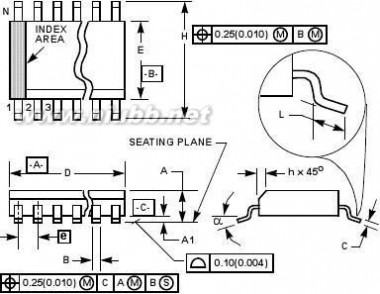
Small Outline Plastic Packages (SOIC)
M14.15 (JEDEC MS-012-AB ISSUE C)
14 LEAD NARROW BODY SMALL OUTLINE PLASTIC PACKAGE
INCHES
SYMBOL
A
MILLIMETERSMIN1.350.100.330.198.553.805.800.250.40
140°
MAX1.750.250.510.258.754.006.200.501.278°
NOTES
--9-34--567-Rev. 0 12/93
MIN0.05320.00400.0130.00750.33670.14970.22840.00990.016
140°
MAX0.06880.00980.0200.00980.34440.15740.24400.01960.0508°
A1BCDEe
0.050 BSC1.27 BSC
HhLN
NOTES:
1.Symbols are defined in the “MO Series Symbol List” in Section 2.2 of Publication Number 95.2.Dimensioning and tolerancing per ANSI Y14.5M-1982.
3.Dimension “D” does not include mold flash, protrusions or gate burrs. Mold flash, protrusion and gate burrs shall not exceed 0.15mm (0.006inch) per side.4.Dimension “E” does not include interlead flash or protrusions. Interlead flash and protrusions shall not exceed 0.25mm (0.010 inch) per side.5.The chamfer on the body is optional. If it is not present, a visual index feature must be located within the crosshatched area.6.“L” is the length of terminal for soldering to a substrate.7.“N” is the number of terminal positions.
8.Terminal numbers are shown for reference only.
9.The lead width “B”, as measured 0.36mm (0.014 inch) or greater above the seating plane, shall not exceed a maximum value of0.61mm (0.024 inch).10.Controlling dimension:MILLIMETER. Converted inch dimensions
are not necessarily exact.
α
11
FN3076.13
December 21, 2005
HFA HFA3096BZ96中文资料
元器件交易网www.cecb2b.com
HFA3046, HFA3096, HFA3127, HFA3128
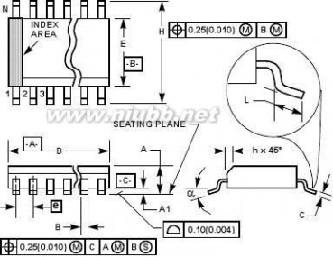
Small Outline Plastic Packages (SOIC)
M16.15 (JEDEC MS-012-AC ISSUE C)
16 LEAD NARROW BODY SMALL OUTLINE PLASTIC PACKAGE
INCHES
SYMBOL
A
MILLIMETERSMIN1.350.100.330.199.803.805.800.250.40
16
8°
0°
8°MAX1.750.250.510.2510.004.006.200.501.27
NOTES
--9-34--567-Rev. 1 6/05
MIN0.05320.00400.0130.00750.38590.14970.22840.00990.016
160°
MAX0.06880.00980.0200.00980.39370.15740.24400.01960.050
A1BCDEeH
0.050 BSC1.27 BSC
hLN
NOTES:
1.Symbols are defined in the “MO Series Symbol List” in Section 2.2 of Publication Number 95.2.Dimensioning and tolerancing per ANSI Y14.5M-1982.
3.Dimension “D” does not include mold flash, protrusions or gate burrs. Mold flash, protrusion and gate burrs shall not exceed 0.15mm (0.006inch) per side.4.Dimension “E” does not include interlead flash or protrusions. Interlead flash and protrusions shall not exceed 0.25mm (0.010 inch) per side.5.The chamfer on the body is optional. If it is not present, a visual index feature must be located within the crosshatched area.6.“L” is the length of terminal for soldering to a substrate.7.“N” is the number of terminal positions.
扩展:3096天 / 3096天 囚室少女 / gb3096 2008
8.Terminal numbers are shown for reference only.
9.The lead width “B”, as measured 0.36mm (0.014 inch) or greater above the seating plane, shall not exceed a maximum value of 0.61mm(0.024 inch).10.Controlling dimension:MILLIMETER. Converted inch dimensions are
not necessarily exact.
α
12
FN3076.13
December 21, 2005
HFA HFA3096BZ96中文资料
元器件交易网www.cecb2b.com
HFA3046, HFA3096, HFA3127, HFA3128
Quad Flat No-Lead Plastic Package (QFN)Micro Lead Frame Plastic Package (MLFP)
Anvil singulation method is used and not present for sawsingulation.
L1e
L
L1
CC
e
L
10.Compliant to JEDEC MO-220VEED-2 Issue C, except for the E2
and D2 MAX dimension.
TERMINAL TIP
All Intersil U.S. products are manufactured, assembled and tested utilizing ISO9000 quality systems.
Intersil Corporation’s quality certifications can be viewed at www.intersil.com/design/quality
Intersil products are sold by description only. Intersil Corporation reserves the right to make changes in circuit design, software and/or specifications at any time withoutnotice. Accordingly, the reader is cautioned to verify that data sheets are current before placing orders. Information furnished by Intersil is believed to be accurate andreliable. However, no responsibility is assumed by Intersil or its subsidiaries for its use; nor for any infringements of patents or other rights of third parties which may resultfrom its use. No license is granted by implication or otherwise under any patent or patent rights of Intersil or its subsidiaries.
For information regarding Intersil Corporation and its products, see www.intersil.com
13
FN3076.13
December 21, 2005
扩展:3096天 / 3096天 囚室少女 / gb3096 2008
三 : NLAST4599中文资料
元器件交易网www.cecb2b.com
NLAST4599
Low Voltage Single SupplySPDT Analog Switch
The NLAST4599 is an advanced high speed CMOS single pole -double throw analog switch fabricated with silicon gate CMOStechnology. It achieves high speed propagation delays and low ONresistances while maintaining low power dissipation. This switchcontrols analog and digital voltages that may vary across the fullpower-supply range (from VCC to GND).
The device has been designed so the ON resistance (RON) is muchlower and more linear over input voltage than RON of typical CMOSanalog switches.
The channel select input structure provides protection when voltagesbetween 0 V and 5.5 V are applied, regardless of the supply voltage. Thisinput structure helps prevent device destruction caused by supply voltage -input/output voltage mismatch, battery backup, hot insertion, etc.
http://onsemi.com

??????????
Select Pin Compatible with TTL Levels
Channel Select Input Over-Voltage Tolerant to 5.5 VFast Switching and Propagation SpeedsBreak-Before-Make Circuitry
Low Power Dissipation: ICC = 2 mA (Max) at TA = 25°CDiode Protection Provided on Channel Select Input
Improved Linearity and Lower ON Resistance over Input VoltageLatch-up Performance Exceeds 300 mA
ESD Performance: HBM > 2000 V; MM > 200 VChip Complexity: 38 FETs
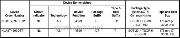
ORDERING INFORMATION
See detailed ordering and shipping information in the packagedimensions section of this data sheet.
SELECT
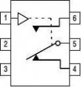
V+GNDNOCOMNC
FUNCTION TABLE
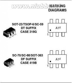
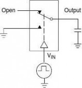
Figure 1. Pin Assignment
SelectLH
ON Channel

NCNO
COM
Figure 2. Logic Symbol
? Semiconductor Components Industries, LLC, 2002
November, 2002 - Rev. 6
CHANNEL SELECTNONC
1
Publication Order Number:
NLAST4599/D
4599 NLAST4599中文资料
元器件交易网www.cecb2b.com
NLAST4599
ABSOLUTE MAXIMUM RATINGS (Note 1)
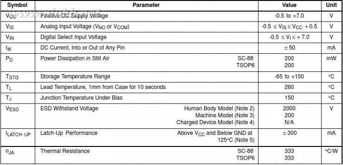

Maximum Ratings are those values beyond which damage to the device may occur. Exposure to these conditions or conditions beyond thoseindicated may adversely affect device reliability. Functional operation under absolute maximum-rated conditions is not implied. Functionaloperation should be restricted to the Recommended Operating Conditions.
1.Maximum Ratings are those values beyond which damage to the device may occur. Functional operation should be restricted to theRecommended Operating Conditions.2.Tested to EIA/JESD22-A114-A3.Tested to EIA/JESD22-A115-A4.Tested to JESD22-C101-A5.Tested to EIA/JESD78
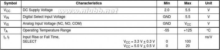
RECOMMENDED OPERATING CONDITIONS
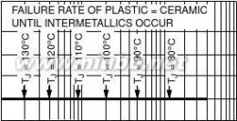
NORMALIZED FAILURE RATE
DEVICE JUNCTION TEMPERATURE VERSUS TIMETO 0.1% BOND FAILURES
100
TIME, YEARS
11
10
1000
Figure 3. Failure Rate vs. Time Junction Temperature
http://onsemi.com
2
4599 NLAST4599中文资料
元器件交易网www.cecb2b.com
NLAST4599
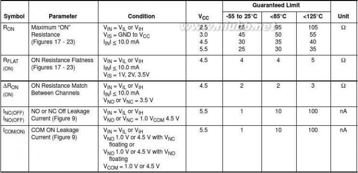
DC CHARACTERISTICS - Digital Section (Voltages Referenced to GND)
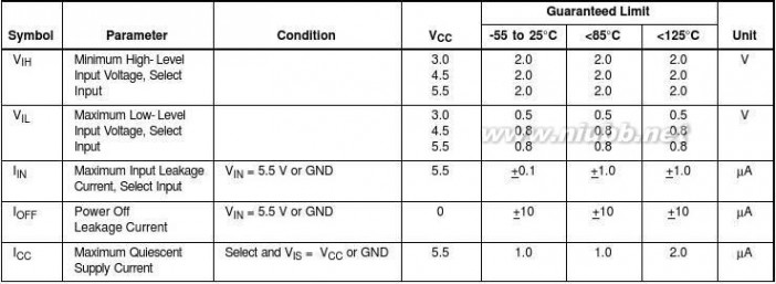
DC ELECTRICAL CHARACTERISTICS - Analog Section
http://onsemi.com
3
4599 NLAST4599中文资料
元器件交易网www.cecb2b.com
NLAST4599
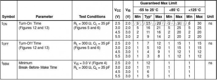
AC ELECTRICAL CHARACTERISTICS (Input t
= t = 3.0 ns)
*Typical Characteristics are at 25_C.
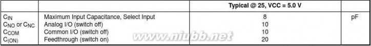
ADDITIONAL APPLICATION CHARACTERISTICS (Voltages Referenced to GND Unless Noted)
http://onsemi.com
4
4599 NLAST4599中文资料
元器件交易网www.cecb2b.com
NLAST4599
VCC

扩展:l298n中文资料 / irf540n中文资料 / irf640n中文资料
0.1 mF
Figure 4. tBBM (Time Break-Before-Make)
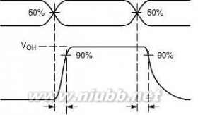

VCC
VCC0.1 mVOUT
Output
VOL
ON
OFF
Input
0 V
Figure 5. tON/tOFF
OFF
ON
Input
Figure 6. tON/tOFF
http://onsemi.com
5
4599 NLAST4599中文资料
元器件交易网www.cecb2b.com
NLAST4599
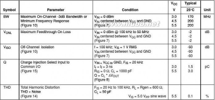
50 ?

?Transmitted
Channel switch control/s test socket is normalized. Off isolation is measured across an off channel. On loss isthe bandwidth of an On switch. VISO, Bandwidth and VONL are independent of the input signal direction.
VOUTVISOIN at 100 kHzIN
VOUTVONLIN at 100 kHz to 50 MHzVIN
ǒBandwidth (BW) = the frequency 3 dB below VONL
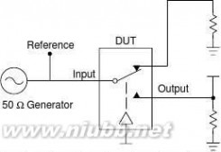
Figure 7. Off Channel Isolation/On Channel Loss (BW)/Crosstalk
(On Channel to Off Channel)/VONL
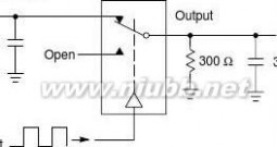
CL
OutputVINVCCGND
Figure 8. Charge Injection: (Q)
100
10
LEAKAGE

(nA)10.10.01
0.001
-55-20257085125
TEMPERATURE (°C)
Figure 9. Switch Leakage vs. Temperature
http://onsemi.com
6
4599 NLAST4599中文资料
元器件交易网www.cecb2b.com
NLAST4599
(dB)
TIME (ns)
1
THD + NOISE (%)
0.1
0.01
110
FREQUENCY (kHz)
100
012
VCOM (V)
345
Figure 14. Total Harmonic Distortion
Plus Noise vs. Frequency
Figure 15. Charge Injection vs. COM Voltage
http://onsemi.com
7

4599 NLAST4599中文资料
元器件交易网www.cecb2b.com
NLAST4599
100101
ICC (nA)
0.10.010.0010.00010.00001
-40
-20
20
60
80
100
120
VIS (VDC)
Temperature (°C)
Figure 16. ICC vs. Temp, VCC = 3 V & 5 V
Figure 17. RON vs. VCC, Temp = 255C
100908070RON (?)
6050403020100RON (?)
0.0
0.5
0.01.01.52.02.53.03.50.51.01.52.02.53.03.54.04.5
VIS (VDC)
VIS (VDC)
Figure 20. RON vs. Temp, VCC = 3.0 V
Figure 21. RON vs. Temp, VCC = 4.5 V
http://onsemi.com
8


4599 NLAST4599中文资料
元器件交易网www.cecb2b.com
NLAST4599
25
20RON (?)
10
5
1500.0
0.51.01.52.02.53.03.54.04.55.0
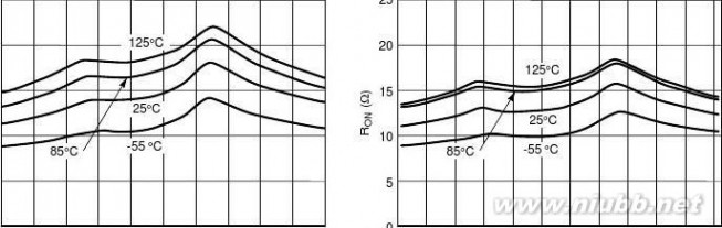
0.00.51.01.52.02.53.03.54.04.55.05.5
VIS (VDC)
VIS (VDC)
Figure 22. RON vs. Temp, VCC = 5.0 VFigure 23. RON vs. Temp, VCC = 5.5 V
DEVICE ORDERING INFORMATION
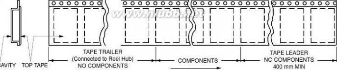
DIRECTION OF FEED
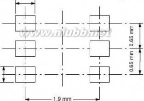
Figure 24. Tape Ends for Finished Goods
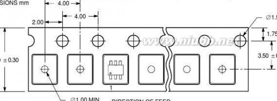
Figure 25. SC70-6/SC-88/SOT-363 DFT2 and SOT23-6/TSOP-6/SC59-6 DTT1 Reel Configuration/Orientation
http://onsemi.com
9
4599 NLAST4599中文资料
元器件交易网www.cecb2b.com
NLAST4599
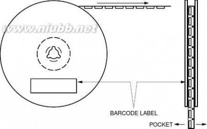
Figure 26. Reel Dimensions
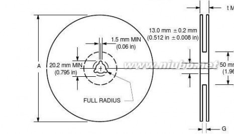
REEL DIMENSIONS
Tape Size8 mm
T and R Suffix
T1, T2
A Max178 mm(7 in)
G
8.4 mm, + 1.5 mm, -0.0(0.33 in + 0.059 in, -0.00)
t Max14.4 mm(0.56 in)
HOLE
Figure 27. Reel Winding Direction
http://onsemi.com
10
4599 NLAST4599中文资料
元器件交易网www.cecb2b.com
NLAST4599
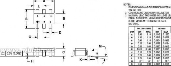
PACKAGE DIMENSIONS
SC70-6/SC-88/SOT-363DF SUFFIXCASE 419B-02
扩展:l298n中文资料 / irf540n中文资料 / irf640n中文资料

NOTES:1.DIMENSIONING AND TOLERANCING PER ANSIY14.5M, 1982.2.CONTROLLING DIMENSION: INCH.3.419B?01 OBSOLETE, NEW STANDARD 419B?02.
http://onsemi.com
11
4599 NLAST4599中文资料
元器件交易网www.cecb2b.com
NLAST4599

PACKAGE DIMENSIONS
SOT23-6/TSOP-6/SC59-6
DT SUFFIXCASE 318G-02
ON Semiconductor and are registered trademarks of Semiconductor Components Industries, LLC (SCILLC). SCILLC reserves the right to makechanges without further notice to any products herein. SCILLC makes no warranty, representation or guarantee regarding the suitability of its products for anyparticular purpose, nor does SCILLC assume any liability arising out of the application or use of any product or circuit, and specifically disclaims any and allliability, including without limitation special, consequential or incidental damages. “Typical” parameters which may be provided in SCILLC data sheets and/orspecifications can and do vary in different applications and actual performance may vary over time. All operating parameters, including “Typicals” must bevalidated for each customer application by customer’s technical experts. SCILLC does not convey any license under its patent rights nor the rights of others.SCILLC products are not designed, intended, or authorized for use as components in systems intended for surgical implant into the body, or other applicationsintended to support or sustain life, or for any other application in which the failure of the SCILLC product could create a situation where personal injury or deathmay occur. Should Buyer purchase or use SCILLC products for any such unintended or unauthorized application, Buyer shall indemnify and hold SCILLCand its officers, employees, subsidiaries, affiliates, and distributors harmless against all claims, costs, damages, and expenses, and reasonable attorney feesarising out of, directly or indirectly, any claim of personal injury or death associated with such unintended or unauthorized use, even if such claim alleges thatSCILLC was negligent regarding the design or manufacture of the part. SCILLC is an Equal Opportunity/Affirmative Action Employer.
PUBLICATION ORDERING INFORMATION
JAPAN: ON Semiconductor, Japan Customer Focus Center2-9-1 Kamimeguro, Meguro-ku, Tokyo, Japan 153-0051Phone: 81-3-5773-3850Email: r14525@onsemi.com
扩展:l298n中文资料 / irf540n中文资料 / irf640n中文资料
四 : DD52RC中文资料
元器件交易网www.cecb2b.com
dd52 DD52RC中文资料
元器件交易网www.cecb2b.com
扩展:stc89c52rc中文资料 / stc90c52rc中文资料 / stc89le52rc中文资料
本文标题:中文资料-SSTA中文资料61阅读| 精彩专题| 最新文章| 热门文章| 苏ICP备13036349号-1