一 : R1114N201B中文资料
元器件交易网www.61k.com
R1114x SERIES LOW NOISE 150mA LDO REGULATOR
NO.EA-094-0512
OUTLINE
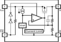
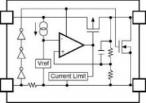
The R1114x Series are CMOS-based voltage regulator ICs with high output voltage accuracy, low supply current, low ON-resistance, and high ripple rejection. Each of these ICs consists of a voltage reference unit, an error amplifier, resistor-net for voltage setting, a current limit circuit, and a chip enable circuit.
These ICs perform with low dropout voltage and a chip enable function. The line transient response and load transient response of the R1114x Series are excellent, thus these ICs are very suitable for the power supply for hand-held communication equipment.
The output voltage of these ICs is fixed with high accuracy. Since the packages for these ICs are SOT-23-5, SC-82AB, and SON1612-6 therefore high density mounting of the ICs on boards is possible.
FEATURES
? Low Supply Current.............................................................Typ. 75μA
? Standby Mode......................................................................Typ. 0.1μA
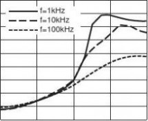
? Low Dropout Voltage............................................................Typ. 0.22V (IOUT=150mA 3.0V Output type) ? High Ripple Rejection..........................................................Typ. 70dB (f=1kHz 3.0V Output type)
.............................................................................................Typ. 60dB (f=10kHz)
? Low Temperature-Drift Coefficient of Output Voltage...........Typ. ±100ppm/°C
? Excellent Line Regulation....................................................Typ. 0.02%/V
? High Output Voltage Accuracy.............................................±2.0%
? Small Packages .................................................................SOT-23-5/SC-82AB/SON1612-6
? Output Voltage.....................................................................Stepwise setting with a step of 0.1V in
the range of 1.5V to 4.0V is possible
? Built-in Fold Back Protection Circuit....................................Typ. 40mA (Current at short mode)
? Ceramic capacitors are recommended to be used with this IC ...CIN=COUT=1μF (VOUT<2.5V)
CIN=1μF, COUT=0.47μF (VOUT>= 2.5V)
APPLICATIONS
? Power source for portable communication equipment.
? Power source for electrical appliances such as cameras, VCRs and camcorders.
? Power source for battery-powered equipment.
1
元器件交易网www.61k.com
R1114x
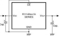
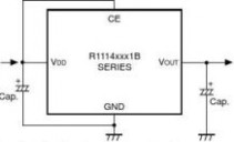
BLOCK DIAGRAMS
R1114xxx1A
R1114xxx1B VOUT

R1114xxx1D VOUT
2
元器件交易网www.61k.com
R1114x
SELECTION GUIDE
The output voltage, version, and the taping type for the ICs can be selected at the user’s request.
The selection can be made with designating the part number as shown below; ←Part Number
↑ ↑ ↑ ↑
a b c d
a Designation of Package Type:
N: SOT-23-5 D: SON1612-6 Q: SC-82AB
b Setting Output Voltage (VOUT):
Stepwise setting with a step of 0.1V in the range of 1.5V to 4.0V is possible.
Designation of Active Type:
c A: active low type
B: active high type
D: active high, with auto discharge
d Designation of Taping Type:
Ex. TR (refer to Taping Specifications; TR type is the standard direction.)
3
元器件交易网www.61k.com
R1114x
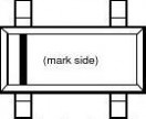
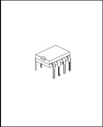
PIN CONFIGURATION
??
SOT-23-5 ??
SC-82AB ??
SON1612-6 54(mark side)
1
1232
1 2 3
PIN DESCRIPTIONS
? R1114Q

? R1114N

? R1114D

4
元器件交易网www.61k.com
R1114x
ABSOLUTE MAXIMUM RATINGS

5
元器件交易网www.61k.com
R1114x
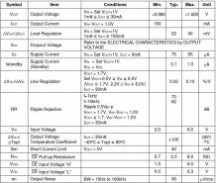
ELECTRICAL CHARACTERISTICS
? R1114xxx1A
6
元器件交易网www.61k.com
R1114x
? R1114xxx1B/D Topt=25°C VOUTVoltage
IOUTCurrent
?VOUT/?IOUT Load Regulation Max.× ×1.020V VIN = Set VOUT+1V 1mA<= IOUT<= 30mA VIN?VOUT = 1.0V VIN = Set VOUT+1V < < 1mA= IOUT= 150mA
VDIFVoltage Refer to the ELECTRICAL CHARACTERISTICS by OUTPUT
VOLTAGE
ISSCurrent VIN = Set VOUT+1V, IOUT = 0mA μA Istandby Supply Current (Standby) VIN = Set VOUT+1V
VCE = GND μA VOUT > 1.7V,
?VOUT/?VIN Line Regulation Set VOUT+0.5V<= VIN<= 6.0V
(VOUT<= 1.7V, 2.2V ≤ VIN<= 6.0V) IOUT = 30mA
f=1kHz 70
f=10kHz 60
Rejection Ripple 0.5Vp?p
VOUT > 1.7V, VIN?VOUT = 1.0V
VOUT<= 1.7, VIN?VOUT = 1.2V
IOUT = 30mA
VINVoltage ?VOUT/?T Output Voltage IOUT = 30mA
Temperature Coefficient ?40°C<= Topt<= 85°C ±100 ppm
/°C
ILIM Short Current Limit VOUT = 0V RPD CE Pull-down ResistanceM? VCEH CE Input Voltage “H”VCEL CE Input Voltage “L”Noise BW = 10Hz to 100kHz μVrms
On Resistance of Nch for
RLOW auto-discharge VCE = 0V ?
(Only for D version)
7
元器件交易网www.61k.com
R1114x
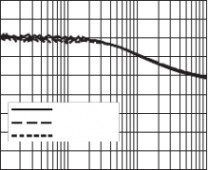
? ELECTRICAL CHARACTERISTICS by OUTPUT VOLTAGE Topt = 25°C Dropout Voltage
Output Voltage VOUT (V)
VOUT = 1.5
VOUT = 1.6
VOUT = 1.7
1.8
2.1
2.8
<= VOUTVDIF (V) IOUT = 150mA <= <= VOUT<= <= VOUT<= 4.0
TECHNICAL NOTES
When using these ICs, consider the following points:
Phase Compensation
In these ICs, phase compensation is made for securing stable operation even if the load current is varied. For this purpose, use a capacitor COUT with good frequency characteristics and ESR (Equivalent Series Resistance). (Note: If additional ceramic capacitors are connected with parallel to the output pin with an output capacitor for phase compensation, the operation might be unstable. Because of this, test these ICs with as same external components as ones to be used on the PCB.)
PCB Layout
Make VDD and GND lines sufficient. If their impedance is high, noise pickup or unstable operation may result. Connect a capacitor with a capacitance value as much as 1.0μF or more between VDD and GND pin, and as close as possible to the pins.
Set external components, especially the output capacitor, as close as possible to the ICs, and make wiring as short as possible.
8
元器件交易网www.61k.com
R1114x
TEST CIRCUITS

FF
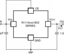
Fig.1 Standard test Circuit Fig.2 Supply Current Test Circuit
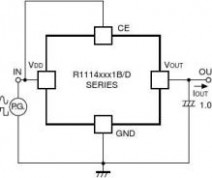
F
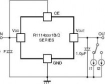
Fig.3 Ripple Rejection, Line Transient Fig.4 Load Transient Response Test Circuit Response Test Circuit
9
元器件交易网www.61k.com
R1114x
TYPICAL APPLICATIONS
IN
(External Components)
Output Capacitor; Ceramic 0.47μF (Set Output Voltage in the range from 2.5 to 4.0V) Ceramic 1.0μF (Set Output Voltage in the range from 1.5 to 2.4V) Input Capacitor; Ceramic 1.0μF
TYPICAL CHARACTERISTICS
1) Output Voltage vs. Output Current (Topt=25°C)
R1114x151x
1.6
R1114x281x
3.0
Output Voltage VOUT(V)
Output Voltage VOUT(V)
1.41.21.00.80.60.40.20.0
100

200
2.52.01.51.00.50.0
300400100
200300400
Output Current IOUT(mA)
Output Current IOUT(mA)
R1114x401x
4.5
Output Voltage VOUT(V)
4.03.53.02.52.01.51.00.50.0
100
200
300
400
10
Output Current IOUT(mA)
元器件交易网www.61k.com
R1114x
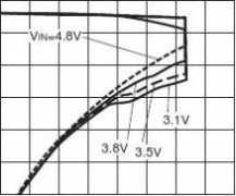
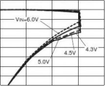
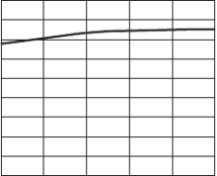
2) Output Voltage vs. Input Voltage (Topt=25°C)
R1114x151x
R1114x281x
1.7
2.9
)
)
2.8V1.6V((TT2.7UUO1.5OVV2.6 1.4 eegg2.5aat1.3tlloo2.4VV t1.2tuu2.3ppttu1.1u2.2OO2.11.0
2.0
1
2
3
4
5
6
2
3
4
5
6
Input Voltage VIN(V)
Input Voltage VIN(V)
R1114x401x
4.2
)
V4.0
(TUOV3.8 egat3.6loV tu3.4ptuO3.23.0
1
2
3
4
5
6
Input Voltage VIN(V)
3) Supply Current vs. Input Voltage (Topt=25°C)
R1114x151x
R1114x281x
909080
)
80
A)
μ(

70Aμ70S(SI60SS I60t nte50nre50rruC40ru C40ylp30 ylpp30
u20pSu2010S100
1
2
3
4
5
6
00
1
2
3
4
5
6
Input Voltage VIN(V)
Input Voltage VIN(V)
11
元器件交易网www.61k.com
R1114x
R1114x401x
90807060504030201000
1
2
3
4
5
6
Supply Current ISS(μA)
Input Voltage VIN(V)
4) Output Voltage vs. Temperature
R1114x151x
1.53
2.86
1.521.511.501.491.481.471.46
-40
-15
10
35
60
85
2.842.822.802.782.762.74
-40
R1114x281x
Output Voltage VOUT(V)
Output Voltage VOUT(V)
-15103560

85
Temperature Topt(°C)
R1114x401x
4.084.064.044.024.003.983.963.943.92
-40
-15
10
35
60
85
Temperature Topt(°C)
Output Voltage VOUT(V)
Temperature Topt(°C)
12
元器件交易网www.61k.com
R1114x
5) Supply Current vs. Temperature
R1114x151x
R1114x281x
90
90
80
)
)
80AAμ70μ((70SSSSI60I60 ttne50ne50rrruC40ruC40 yl30 ylpp30pu20puS20S101000-40
-15
10
35
60
85
-40
-15103560
85
Temperature Topt(°C)
Temperature Topt(°C)
R1114x401x
90)
80Aμ(70SSI 60tne50rruC40 ylp30puS20100-40
-15
10
35
60
85
Temperature Topt(°C)
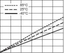
6) Dropout Voltage vs. Temperature
R1114x151x
R1114x161x
0.6
0.6
)
V(0.5)
V(0.5FFIIDDV0.4V 0.4eegga0.3attlloo0.3VV t0.2tuuoo0.2ppoor0.1rDD0.10.0
25
5075
1001251500.0
25
5075100125150
Output Current IOUT(mA)
Output Current IOUT(mA)
13
元器件交易网www.61k.com
R1114x
R1114x171x
0.6
R1114x181x
0.6
Dropout Voltage VDIF(V)

Dropout Voltage VDIF(V)
0.50.40.30.20.10.0
25
0.50.40.30.20.10.0
25
5075100125150
5075100125150
0.40
Output Current IOUT(mA)
Output Current IOUT(mA)
R1114x211x
0.40
R1114x281x
Dropout Voltage VDIF(V)
0.350.300.250.200.150.100.050.00
25
50
75
100
125
150
Dropout Voltage VDIF(V)
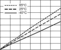
0.350.300.250.200.150.100.050.00
25
5075100125150
0.40
Output Current IOUT(mA)
Output Current IOUT(mA)
R1114x401x
Dropout Voltage VDIF(V)
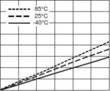
0.350.300.250.200.150.100.050.00
25
50
75
100
125
150
Output Current IOUT(mA)
14
元器件交易网www.61k.com
R1114x
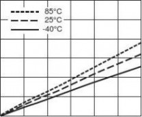
7) Dropout Voltage vs. Set Output Voltage (Topt=25°C)
0.60
)
V(0.50FIDV 0.40egatlo0.30V tuo0.20porD0.100.00
1.0
1.52.02.5
3.03.54.0
Set Output Voltage VREG(V)
8) Ripple Rejection vs. Input Bias Voltage (Topt=25°C, CIN=none, COUT=ceramic0.47μF)
R1114x281x
R1114x281x
90
Ripple 0.2Vp-p, IOUT=1mA
90
Ripple 0.5Vp-p, IOUT=1mA
)
80)
80BB
dd(70(70RRRR 6060 nnooiit5050tcceejje40e40RR e30e30llp20pppiiR1020R10002.9
3.0
3.1
3.2
3.3
2.9
3.0
3.1
3.2
3.3
Input Voltage VIN(V)
Input Voltage VIN(V)
R1114x281x
R1114x281x
90
OUT90
OUT)
80
)
80BBdd(70(70RRRR60 60 nnooi50i50ttcceejje40e40R e30R e30llpp20pp20iiR10R100

2.9
3.0
3.1
3.2
3.3
2.9
3.0
3.1
3.2
3.3
Input Voltage VIN(V)
Input Voltage VIN(V)
15
元器件交易网www.61k.com
R1114x
R1114x281x
90
Ripple 0.2Vp-p, IOUT=50mA
90
807060504030201002.9
3.0
3.1
3.2
3.3
807060504030201002.9
3.0
3.1
3.2
3.3
R1114x281x
Ripple 0.5Vp-p, IOUT=50mARipple Rejection RR(dB)
Input Voltage VIN(V)
Ripple Rejection RR(dB)
Input Voltage VIN(V)
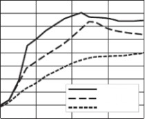
9) Ripple Rejection vs. Frequency (CIN=none)
R1114x151x
90
VIN=2.5VDC+0.5Vp-p,COUT=Ceramic 1.0μF
90
R1114x151x
VIN=2.5VDC+0.5Vp-p,COUT=Ceramic 2.2μF
Ripple Rejection RR(dB)

Ripple Rejection RR(dB)
807060504030201000.1
1
10
100
807060504030201000.1
1
10
100
Frequency f(kHz)
R1114x281x
90
VIN=3.8VDC+0.5Vp-p,COUT=Ceramic 0.47μF
90
Frequency f(kHz)
R1114x281x
VIN=3.8VDC+0.5Vp-p,COUT=Ceramic 1.0μF
Ripple Rejection RR(dB)

7060504030201000.1
1
10
100
Ripple Rejection RR(dB)
80807060504030201000.1
1
10
100
Frequency f(kHz)
Frequency f(kHz)
16
元器件交易网www.61k.com
R1114x
R1114x401x R1114x401x
VIN=5.0VDC+0.5Vp-p,VIN=5.0VDC+0.5Vp-p,
90COUT=Ceramic 0.47μF90COUT=Ceramic 1.0μF
)

80)
80
B
d
(70Bd(70
RR 60RR 60
no
i50
t50noi
t
ce
je40ceje40
R30R
ee30llp20p
pp20iiR10R10
00
0.11101000.1110100
Frequency f(kHz) Frequency f(kHz)
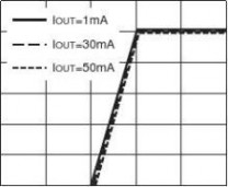
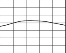
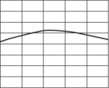
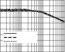
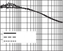
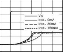
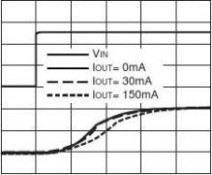
10) Input Transient Response (IOUT=30mA, CIN=none, tr=tf=5μs, COUT=Ceramic 0.47μF)
R1114x151x
1.554
)V1.543
()
TVU(
ON
I
V1.532V
ee
gg
aa
t1.521t
ll
oo
VV
tt
u1.510u
pp
t
un
I
O1.501.49010203040

5060708090100
Time T(μs)
R1114x281x
2.856
)V2.845
()
TVU(
ON
I
V2.834V
ee
gg
aa

t2.823t
ll
oo
VV
tt
u2.812u
pp
tun
I
O2.801
2.790
0102030405060708090100
Time T(μs)
17
元器件交易网www.61k.com
R1114x
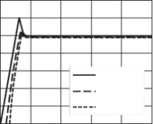
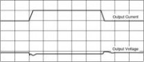
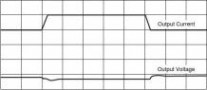
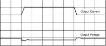
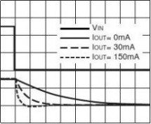
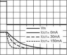
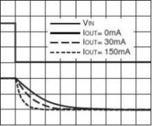
11) Load Transient Response (tr=tf=0.5μs, CIN=Ceramic 1.0μF)
R1114x151x
1.75
VIN=2.5V, COUT=Ceramic 1.0μF
150
1.651.601.551.501.45
500
02468101214161820
Time T(μs)
Output Current IOUT(mA)
Output Voltage VOUT(V
)
1.70100
R1114x151x
1.75
VIN=2.5V, COUT=Ceramic 2.2μF
150
1.651.601.551.501.45
500
02468101214161820
Time T(μs)
Output Current IOUT(mA)
Output Voltage VOUT(V
)
1.70100
R1114x281x
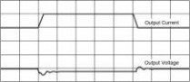
3.05
INOUT150
2.952.902.852.802.75
500
02468101214161820
Time T(μs)
Output Current IOUT(mA)
Output Voltage VOUT(V)
3.00100
18
元器件交易网www.61k.com
R1114x
R1114x281x
3.05INOUT150
))
V3.00100A
(Tm
U(
O2.9550T
UVO
I
e
t
g2.900n
ae
trl
or
Vu
t
u2.85C
t
pu
t
up
t
O2.80uO
2.7502468101214161820
Time T(μs)
R1114x281x

3.05VIN=3.8V, COUT=Ceramic 2.2F150
))
V3.00100A
(Tm
U(
O2.9550T
UVO
I
e t
g
at2.900nerl
or
Vu
tu2.85C
t
pu
tput
O2.80uO
2.7502468101214161820
Time T(μs)
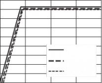
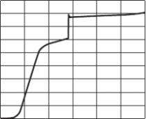
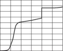
12) Turn-on/off speed with CE pin (D version)
R1114x151D (VIN=2.5V, CIN=Ceramic 1.0μF, COUT=Ceramic 1.0μF)
4646
)3
5))VVV35)((V
E((CTET2UCVU 4OV24OV eVg1 e
egaet3ga13g
lat
loa
tt
V02lo
oV02lo
t
uV
tV
p1tu
nup1t
u
Ipnp
tItEu uC0OEC0
O
-50510152025-50050100150200250300350400450
Time T(μs) Time T(μs)
19
元器件交易网www.61k.com
R1114x
R1114x281D (VIN=3.8V, CIN=Ceramic 0.47μF, COUT=Ceramic 0.47μF)
4
8
4
865
43210
-200
20406080100120140160180
CE Input Voltage VCE(V)
CE Input Voltage VCE(V)
Output Voltage VOUT(V)

210-1
6543210
210-1
-50510152025
8
Time T(μs)
Time T(μs)
Output Voltage VOUT(V)
3737
R1114x401D (VIN=5.0V, CIN=Ceramic 0.47μF, COUT=Ceramic 0.47μF)
14
8
14
CE Input Voltage VCE(V)
CE Input Voltage VCE(V)
Output Voltage VOUT(V)
420-2
1086420
420-2
1086420
-50510152025
-2
-200
-2
20406080100120140160180
Time T(μs)
Time T(μs)
Output Voltage VOUT(V)
612612
20

二 : XN0611FH中文资料
Composite Transistors
Publication date: July 2003
SJJ00099BED
1
n0611 XN0611FH中文资料
XN0611FH
■Electrical Characteristics Ta = 25°C ± 3°C
?Tr1
Parameter
Collector-base voltage (Emitter open)Collector-emitter voltage (Base open)Collector-base cutoff current (Emitter open)Collector-emitter cutoff current (Base open)Emitter-base cutoff current (Collector open)Forward current transfer ratioCollector-emitter saturation voltageOutput voltage high-levelOutput voltage low-levelInput resistanceResistance ratioTransition frequency
SymbolVCBOVCEOICBOICEOIEBOhFEVCE(sat)VOHVOLR1R1 / R2fT
VCB = ?10 V, IE = 1 mA, f = 200 MHz
Conditions
IC = ?10 μA, IE = 0IC = ?2 mA, IB = 0VCB = ?50 V, IE = 0VCE = ?50 V, IB = 0VEB = ?6 V, IC = 0VCE = ?10 V, IC = ?5 mAIC = ?10 mA, IB = ? 0.3 mAVCC = ?5 V, VB = ? 0.5 V, RL = 1 k?VCC = ?5 V, VB = ?2.5 V, RL = 1 k?
?30%
4.70.4780
?4.9
? 0.2+30%
30
? 0.25
Min?50?50
? 0.1? 0.5?1.0
Typ
Max
UnitVVμAμAmA?VVVk??MHz
Note)Measuring methods are based on JAPANESE INDUSTRIAL STANDARD JIS C 7030 measuring methods for transistors.
?Tr2
Parameter
Collector-base voltage (Emitter open)Collector-emitter voltage (Base open)Collector-base cutoff current (Emitter open)Collector-emitter cutoff current (Base open)Emitter-base cutoff current (Collector open)Forward current transfer ratioCollector-emitter saturation voltageOutput voltage high-levelOutput voltage low-levelInput resistanceResistance ratioTransition frequency
SymbolVCBOVCEOICBOICEOIEBOhFEVCE(sat)VOHVOLR1R1 / R2fT
VCB = ?10 V, IE = 1 mA, f = 200 MHz
Conditions
IC = ?10 μA, IE = 0IC = ?2 mA, IB = 0VCB = ?50 V, IE = 0VCE = ?50 V, IB = 0VEB = ?6 V, IC = 0VCE = ?10 V, IC = ?5 mAIC = ?10 mA, IB = ? 0.3 mAVCC = ?5 V, VB = ? 0.5 V, RL = 1 k?VCC = ?5 V, VB = ?2.5 V, RL = 1 k?
?30%0.17
2.20.2280
?4.9
? 0.2+30%0.27
30
? 0.25
Min?50?50
? 0.1? 0.5? 0.5
Typ
Max
UnitVVμAμAmA?VVVk??MHz
Note)Measuring methods are based on JAPANESE INDUSTRIAL STANDARD JIS C 7030 measuring methods for transistors.
2
SJJ00099BED
n0611 XN0611FH中文资料
XN0611FH
SJJ00099BED
3
n0611 XN0611FH中文资料

4
SJJ00099BED
n0611 XN0611FH中文资料
Request for your special attention and precautions in using the technical information
and semiconductors described in this material
(1)An export permit needs to be obtained from the competent authorities of the Japanese Governmentif any of the products or technologies described in this material and controlled under the "ForeignExchange and Foreign Trade Law" is to be exported or taken out of Japan.
(2)The technical information described in this material is limited to showing representative characteris-tics and applied circuits examples of the products. It neither warrants non-infringement of intellec-tual property right or any other rights owned by our company or a third party, nor grants any license.
(3)We are not liable for the infringement of rights owned by a third party arising out of the use of theproduct or technologies as described in this material.
(4)The products described in this material are intended to be used for standard applications or generalelectronic equipment (such as office equipment, communications equipment, measuring instru-ments and household appliances).
Consult our sales staff in advance for information on the following applications:
?Special applications (such as for airplanes, aerospace, automobiles, traffic control equipment,combustion equipment, life support systems and safety devices) in which exceptional quality andreliability are required, or if the failure or malfunction of the products may directly jeopardize life orharm the human body.
?Any applications other than the standard applications intended.
(5)The products and product specifications described in this material are subject to change withoutnotice for modification and/or improvement. At the final stage of your design, purchasing, or use ofthe products, therefore, ask for the most up-to-date Product Standards in advance to make sure thatthe latest specifications satisfy your requirements.
(6) When designing your equipment, comply with the guaranteed values, in particular those of maxi-mum rating, the range of operating power supply voltage, and heat radiation characteristics. Other-wise, we will not be liable for any defect which may arise later in your equipment.
扩展:tmp86fh09ang中文资料 / x5045中文资料 / prtr5v0u2x中文资料
Even when the products are used within the guaranteed values, take into the consideration ofincidence of break down and failure mode, possible to occur to semiconductor products. Measureson the systems such as redundant design, arresting the spread of fire or preventing glitch arerecommended in order to prevent physical injury, fire, social damages, for example, by using theproducts.
(7) When using products for which damp-proof packing is required, observe the conditions (includingshelf life and amount of time let standing of unsealed items) agreed upon when specification sheetsare individually exchanged.
(8) This material may be not reprinted or reproduced whether wholly or partially, without the prior writtenpermission of Matsushita Electric Industrial Co., Ltd.
2002 JUL
扩展:tmp86fh09ang中文资料 / x5045中文资料 / prtr5v0u2x中文资料
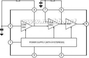
三 : UTC31001中文资料
元器件交易网www.cecb2b.com
UTC31001 LINEAR INTEGRATEDCIRCUIT
TELEPHONE TONE RINGER
GENERAL DESCRIPTION
The UTC 31001 is a bipolar integrated circuit
designed for telephone bell replacement. It can also beused as alarms or other alerting devices.
FEATURES
*Designed for telephone bell replacement.
*Low current drain for multiple extention of lines.*Adjustable 2-frequency tone.*Adjustable warbling rate.
*Bulit-in hysteresis prevents false triggering and rotary dial 'CHIRPS'.
*Programmable for initiation voltage by simple external resistor
BLOCK DIAGRAM
C2
externally mounted
CHARACTERISTIC
Supply Voltage
Power Dissipation
Operating Temperature Storage Temperature
Note:R2,R3,C2 and C3 are parts
ABSOLUTE MAXIMUM RATINGS(Ta=25°C )
SYMBOL Vcc Pd Topr Tstg
VALUE30400-45 to 85-65 to 150
UNITVmW
°CUTC UNISONIC TECHNOLOGIES CO. LTD
1
31001 UTC31001中文资料
元器件交易网www.cecb2b.com
UTC31001 LINEAR INTEGRATEDCIRCUIT
ELECTRICAL CHARACTERISTICS( Ta=25°C )
(All voltage referenced to GND unless otherwise specified)
CHARACTERISTIC
Operating Supply Voltage
Initiation Supply Voltage (note 1) Initiation Supply Current (note 1) Sustaining Voltage (note 2) Sustaining Current (note 2) Output Voltage High Output Voltage Low IIN(Pin3) IIN(pin7)
High Frequency 1 High Frequency 2 Low Frequency
SYMBOL Vcc Vsi Isi Vsus Isus VOH VOL
TEST CONDITIONSee Fig.2
6.8K-Pin 2 to GND
See Fig.2
No Load Vcc=Vsus,See Fig.2
Vcc=21V, I8=-15mAPin6=6V, Pin7=GNDVcc=21V, I8=15mAPin6=GND, Pin7=6VPin3=6V, Pin4=GNDPin7=6V, Pin6=GNDR3=191K, C3=6800pFR3=191K, C3=6800pFR2=165K, C2=0.47μF
MIN171.49.70.717.0
TYP.193.511.01.419.0
MAX29.0214.212.02.521.01.650050056370411.0

UNITVVmAVmAVVnAnAHzHzHz
FH1 FH2 FL4615769.051264010
*NOTE (See electrical characteristics sheet)
1. Initiation supply voltage (Vsi) is the supply voltage required to start the tone ringer oscillating. 2. Sustaining voltage (Vsus) is the supply voltage required to maintain oscillation.
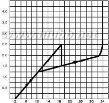
Circuit Current-Supply Voltage
Supply Current Vs. Supply Voltage
Supply Current (mA)
Vcc(V),Supply voltageVcc(V),Supply voltage
Fig.2 Fig. 3
UTC UNISONIC TECHNOLOGIES CO. LTD
2
31001 UTC31001中文资料
元器件交易网www.cecb2b.com
UTC31001 LINEAR INTEGRATEDCIRCUIT
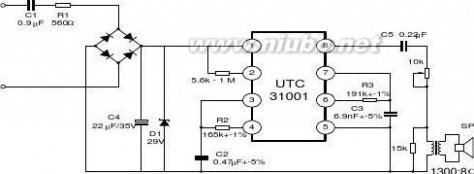
APPLICATION CIRCUIT
TIP
RING
Fig.4
UTC UNISONIC TECHNOLOGIES CO. LTD
3
扩展:utc3842d中文资料 / utc358中文资料 / utc78m12中文资料
四 : SE95中文资料


元器件交易网www.cecb2b.com
se95se SE95中文资料
se95se SE95中文资料
se95se SE95中文资料
se95se SE95中文资料
se95se SE95中文资料
se95se SE95中文资料
se95se SE95中文资料
元器件交易网www.cecb2b.com
Philips Semiconductors
Product data sheet
Ultra high accuracy digital temperature sensor andSE95
thermal Watchdog?
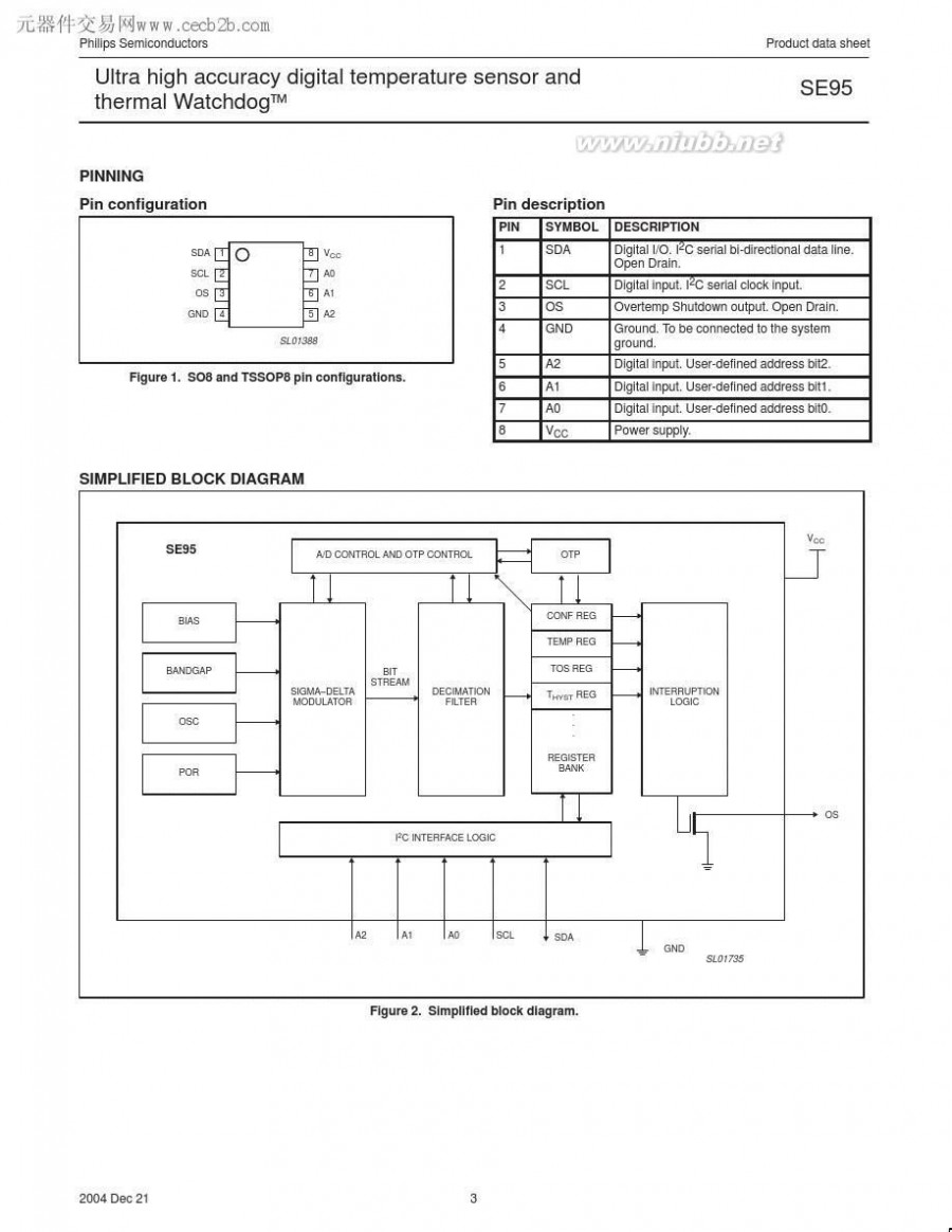
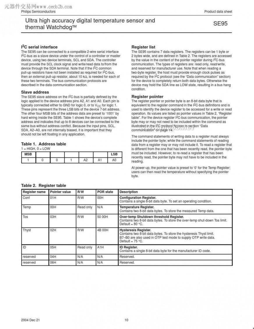
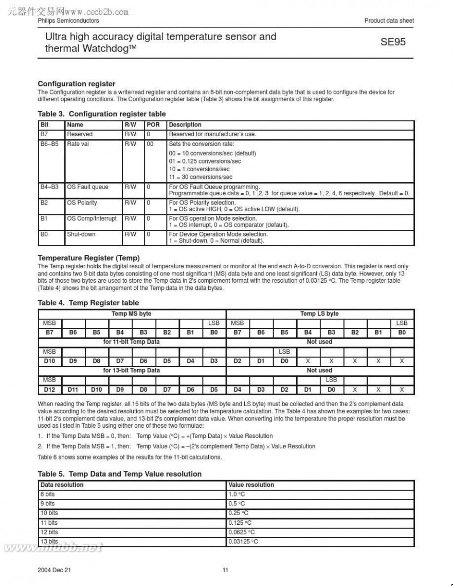
FUNCTIONAL DESCRIPTIONGeneral operation
The SE95 uses the on-chip band-gap sensor to measure the devicetemperature with the resolution of 0.03125 °C and stores the 13-bit2’s complement digital data, resulted from 13-bit A-to-D conversion,into the device Temp register. This Temp register can be read at anytime by a controller on the I2C-bus. Reading temperature data doesnot affect the conversion in progress during the read operation.The device can be set to operate in either mode: normal or
shut-down. In normal operation mode, by default, the temp-to-digitalconversion is executed every 100 ms and the Temp register isupdated at the end of each conversion. In shut-down mode, thedevice becomes idle, data conversion is disabled and the Tempregister holds the latest result; however, the device I2C interface isstill active and register write/ read operation can be performed. Thedevice operation mode is controlled by programming bit B0 of theconfiguration register. The temperature conversion is initiated whenthe device is powered up or returned to normal mode fromshut-down.
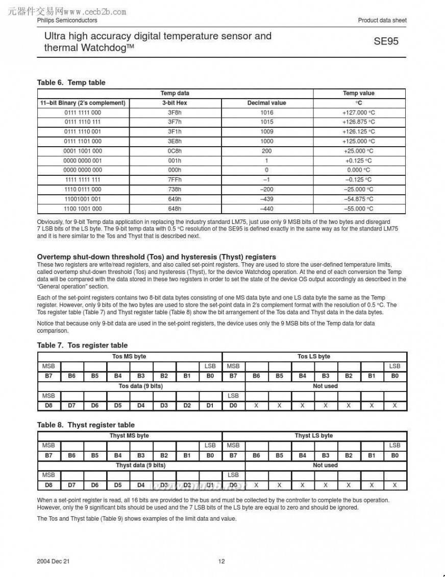
In addition, at the end of each conversion in normal mode, thetemperature data (or Temp) in the Temp register is automaticallycompared with the over-temp shut-down threshold data (or Tos)stored in the Tos register, and the hysteresis data (or Thyst) storedin the Thyst register, in order to set the state of the device OS outputaccordingly. The device Tos and Thyst registers are write/readcapable, and both operate with 9-bit 2’s complement digital data.To match with this 9-bit operation, the temp register uses only the9 MSB bits of its 13-bit data for the comparison.
The device temperature conversion rate is programmable and canbe chosen to be one of the four values: 0.125, 1.0, 10, and 30conversions per second. The default conversion rate is 10conversions per second. Furthermore, the conversion rate isselected by programming bits B5 and B6 of the Configuration
Register as shown in Table 3. Note that the average supply currentas well as the device power consumption increase with theconversion rate.
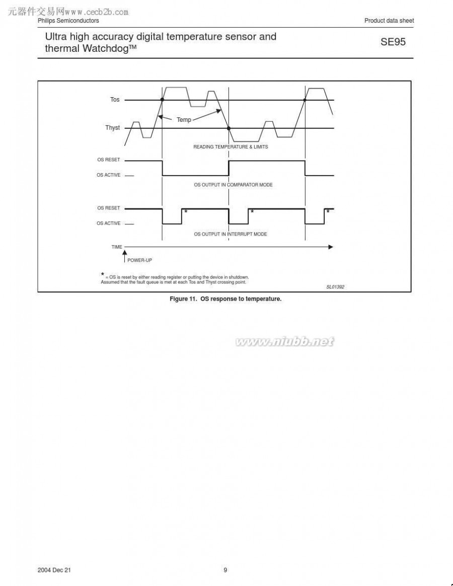
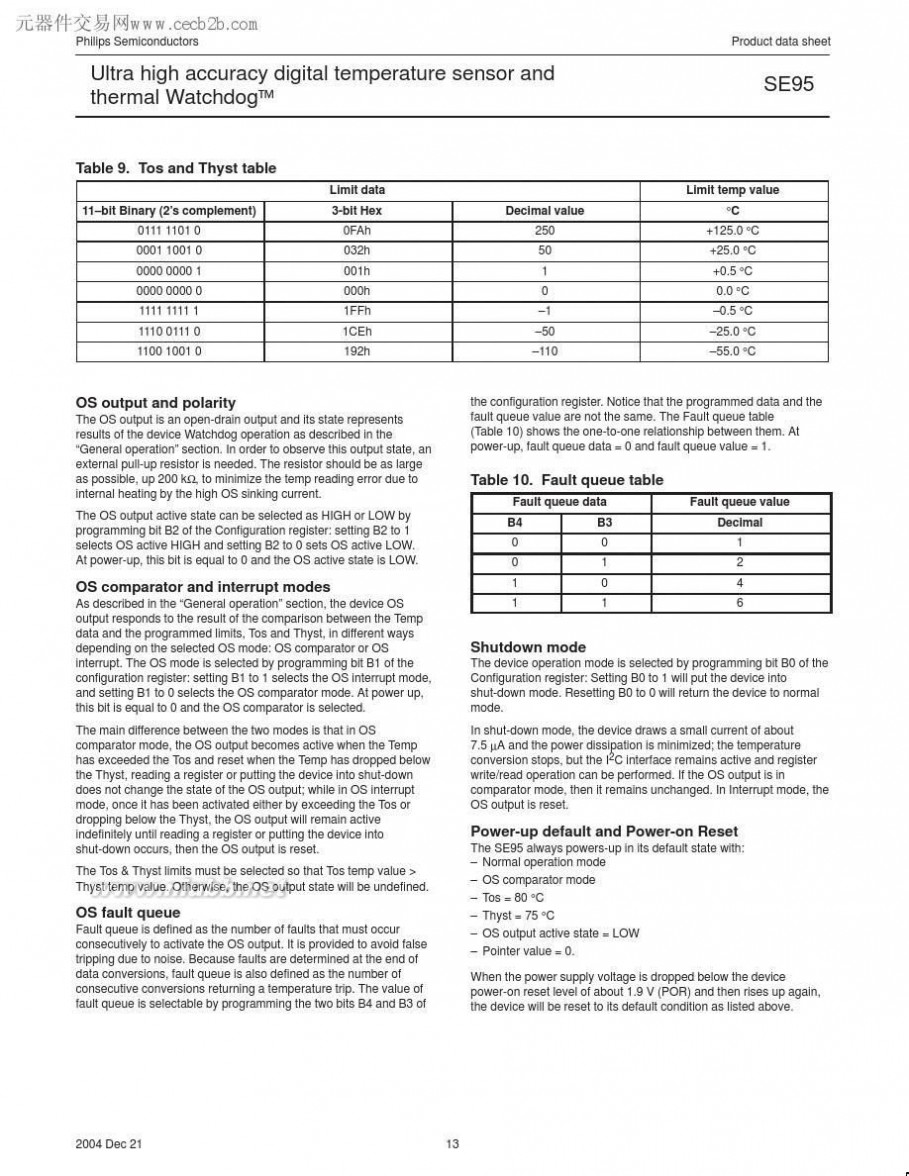
2004 Dec 21The way that the OS output responds to the comparison operationdepends upon the OS operation mode selected by configurationbit B1, and the user-defined fault queue defined by configurationbits B3 and B4.
In OS comparator mode, the OS output behaves like a thermostat. Itbecomes active when the Temp exceeds the Tos, and is reset whenthe Temp drops below the Thyst. Reading the device registers orputting the device into shut-down does not change the state of theOS output. The OS output in this case can be used to controlcooling fans or thermal switches.
In OS interrupt mode, the OS output is used for thermal interruption.When the device is powered-up, the OS output is first activated onlywhen the Temp exceeds the Tos; then it remains active indefinitelyuntil being reset by a read of any register. Once the OS output hasbeen activated by crossing Tos and then reset, it can be activatedagain only when the Temp drops below the Thyst; then again, it
remains active indefinitely until being reset by a read of any register.The OS interrupt operation would be continued in this sequence:Tos trip, Reset, Thyst trip, Reset, Tos trip, Reset, Thyst trip, Reset,and etc. Putting the device into shut-down mode also resets the OSoutput.
In both cases, comparator mode and interrupt mode, the OS outputis activated only if a number of consecutive faults, defined by thedevice fault queue, has been met. The fault queue is programmableand stored in the two bits, B3 and B4, of the Configuration register.Also, the OS output active state is selectable as HIGH or LOW bysetting accordingly the configuration register bit B2.
扩展:mb95f564k中文资料 / ss495a1中文资料 / mb95f636 中文资料
At power-up, the device is put into normal operation mode, the Tosis set to 80 °C, the Thyst is set to 75 °C, the OS active state isselected LOW and the fault queue is equal to 1. The temp readingdata is not available until the first conversion is completed in about33 ms.
The OS response to the temperature is illustrated in Figure 11.
8
se95se SE95中文资料
se95se SE95中文资料
se95se SE95中文资料
se95se SE95中文资料
se95se SE95中文资料
se95se SE95中文资料
元器件交易网www.cecb2b.com
Philips Semiconductors
Product data sheet
Ultra high accuracy digital temperature sensor andSE95
thermal Watchdog?
Data communication
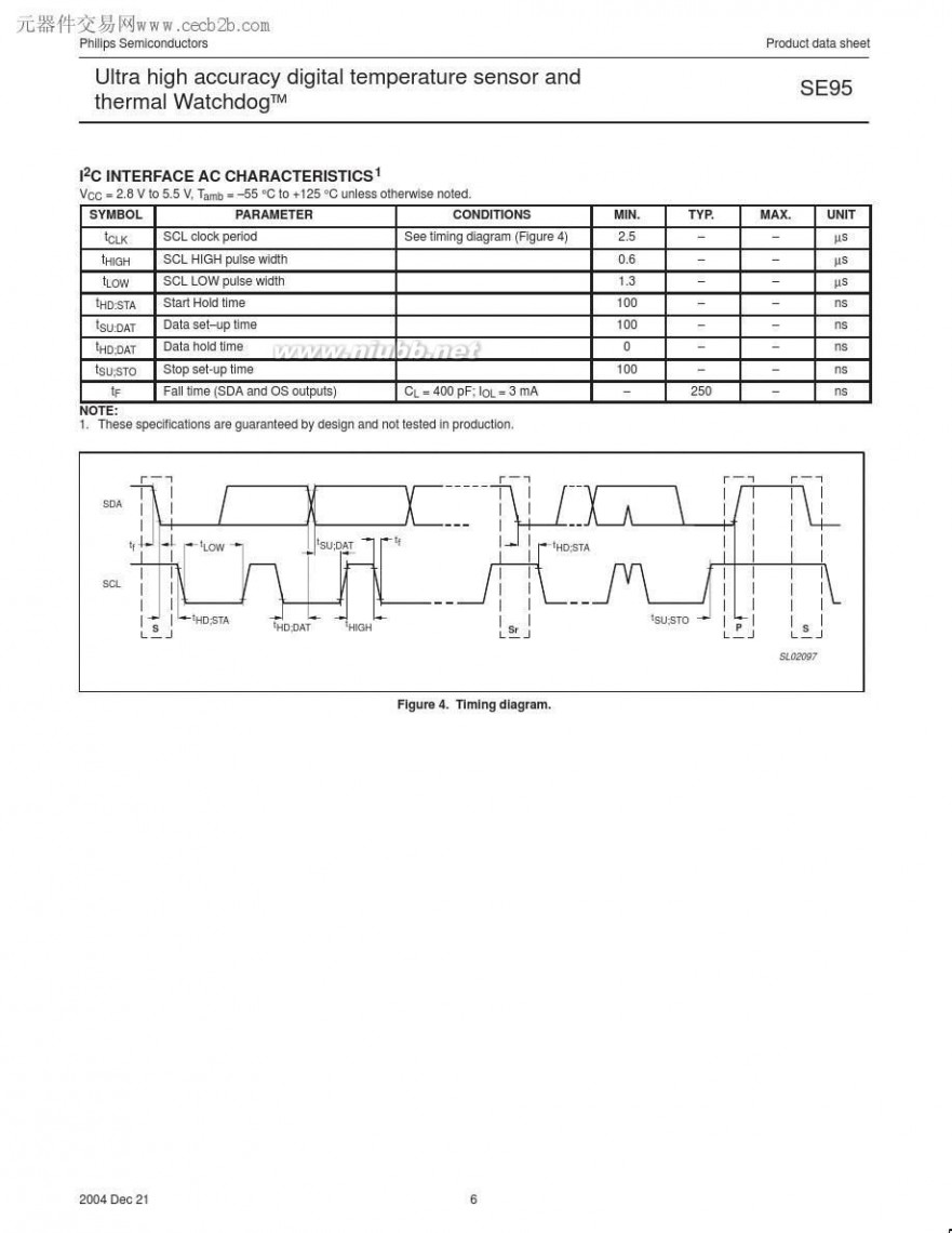
The communication between the host and the SE95 must strictlyfollow the rules as defined by the I2C-bus management. The
protocols for SE95 register read/write operations are illustrated bythe Figures as follows with these definitions:
1.Before a communication, the I2C-bus must be free or not busy. It
means that the SCL and SDA lines must be both released by alldevices on the bus, and they become HIGH by the bus pull-upresistors.2.The host must provide SCL clock pulses necessary for the
communication. Data is transferred in sequence of 9 SCL clockpulses for every 8-bit data byte followed by 1-bit status of theacknowledgement.3.During data transfer, except the Start and Stop signals, the SDA
signal must be stable while the SCL signal is HIGH. It meansthat SDA signal can be changed only during the LOW durationof the SCL line.4.S: Start signal, initiated by the host to start a communication,
the SDA goes from HIGH-to-LOW while the SCL is HIGH.5.RS: Re-start signal, same as the Start signal, to start a read
command that follows a write command.6.P: Stop signal, generated by the host to stop a communication,
the SDA goes from LOW-to-HIGH while the SCL is HIGH. Thebus becomes free thereafter.
2004 Dec 217.W: Write bit, when the Write/Read bit = LOW in a write
command.8.R: Read bit, when the Write/Read bit = HIGH in a read
command.9.A: Device Acknowledge bit, returned by the SE95. It is LOW if
the device works properly and HIGH if not. The host mustrelease the SDA line during this period in order to give thedevice the control on the SDA line.10.A′: Master Acknowledge bit, not returned by the device, but set
by the master or host in reading 2-byte data. During this clockperiod, the host must set the SDA line to LOW in order to noticethe device that the first byte has been read for the device toprovide the second byte onto the bus.11.NA: Not-Acknowledge bit. During this clock period, both the
device and host release the SDA line at the end of a datatransfer, the host is then enabled to generate the Stop signal.12.In a write protocol, data is sent from the host to the device and
the host controls the SDA line, except during the clock periodwhen the device sends to the bus the device acknowledgementsignal.13.In a read protocol, data is sent to the bus by the device and the
host must release the SDA line during the time that the device isproviding data onto the bus and controlling the SDA line, exceptduring the clock period when the master sends to the bus themaster acknowledgement signal.
14
se95se SE95中文资料

se95se SE95中文资料

se95se SE95中文资料
元器件交易网www.cecb2b.com
Philips SemiconductorsProduct data sheetUltra high accuracy digital temperature sensor and
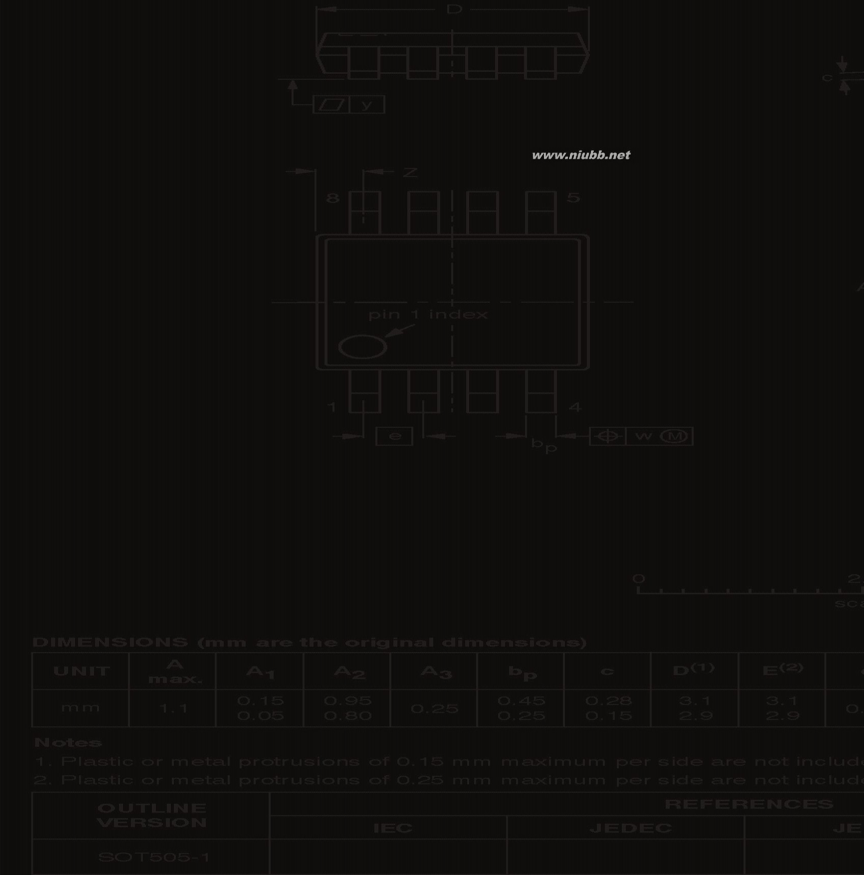
thermal Watchdog?SE95SO8:plastic small outline package; 8 leads; body width 3.9 mmSOT96-12004 Dec 2117
se95se SE95中文资料
元器件交易网www.cecb2b.com
Philips SemiconductorsProduct data sheetUltra high accuracy digital temperature sensor and
thermal Watchdog?SE95TSSOP8:plastic thin shrink small outline package; 8 leads; body width 3 mmSOT505-12004 Dec 2118
扩展:mb95f564k中文资料 / ss495a1中文资料 / mb95f636 中文资料
se95se SE95中文资料
se95se SE95中文资料
元器件交易网www.cecb2b.com
Philips SemiconductorsProduct data sheetUltra high accuracy digital temperature sensor and
thermal Watchdog?


SE95
Definitions
Short-form specification — The data in a short-form specification is extracted from a full data sheet with the same type number and title. For detailed information seethe relevant data sheet or data handbook.
Limiting values definition — Limiting values given are in accordance with the Absolute Maximum Rating System (IEC 60134). Stress above one or more of the limitingvalues may cause permanent damage to the device. These are stress ratings only and operation of the device at these or at any other conditions above those givenin the Characteristics sections of the specification is not implied. Exposure to limiting values for extended periods may affect device reliability.
Application information — Applications that are described herein for any of these products are for illustrative purposes only. Philips Semiconductors make norepresentation or warranty that such applications will be suitable for the specified use without further testing or modification.
Disclaimers
Life support — These products are not designed for use in life support appliances, devices, or systems where malfunction of these products can reasonably beexpected to result in personal injury. Philips Semiconductors customers using or selling these products for use in such applications do so at their own risk and agreeto fully indemnify Philips Semiconductors for any damages resulting from such application.
Right to make changes — Philips Semiconductors reserves the right to make changes in the products—including circuits, standard cells, and/or software—describedor contained herein in order to improve design and/or performance. When the product is in full production (status ‘Production’), relevant changes will be communicatedvia a Customer Product/Process Change Notification (CPCN). Philips Semiconductors assumes no responsibility or liability for the use of any of these products, conveysno license or title under any patent, copyright, or mask work right to these products, and makes no representations or warranties that these products are free from patent,copyright, or mask work right infringement, unless otherwise specified.
Contact information
For additional information please visit
http://www.semiconductors.philips.com.Fax: +31 40 27 24825? Koninklijke Philips Electronics N.V. 2004All rights reserved. Published in the U.S.A.
Date of release: 12-04
For sales offices addresses send e-mail to:
Document number:9397 750 14388
扩展:mb95f564k中文资料 / ss495a1中文资料 / mb95f636 中文资料
五 : PT6621中文资料


元器件交易网www.cecb2b.com
48
Power Trends, Inc. 27715 Diehl Road, Warrenville, IL 60555 (800) 531-5782 Fax: (630) 393-6902 http://www.powertrends.com
6621 PT6621中文资料


元器件交易网www.cecb2b.com
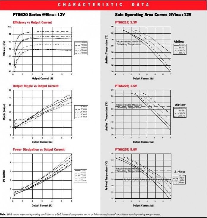
** See SOA curves - Output power is limited to 30W maximum.
Note: The PT6620 Series requires a 330μF(output) and 100μF(input) electrolytic capacitors for proper operation in all applications.
Power Trends, Inc. 27715 Diehl Road, Warrenville, IL 60555 (800) 531-5782 Fax: (630) 393-6902 http://www.powertrends.com
49
6621 PT6621中文资料
元器件交易网www.cecb2b.com
For assistance or to order, call
(800) 531-5782
6621 PT6621中文资料
元器件交易网www.cecb2b.com
For assistance or to order, call
(800) 531-5782
6621 PT6621中文资料
元器件交易网www.cecb2b.com
IMPORTANT NOTICE
Texas Instruments and its subsidiaries (TI) reserve the right to make changes to their products or to discontinueany product or service without notice, and advise customers to obtain the latest version of relevant informationto verify, before placing orders, that information being relied on is current and complete. All products are soldsubject to the terms and conditions of sale supplied at the time of order acknowledgement, including thosepertaining to warranty, patent infringement, and limitation of liability.
TI warrants performance of its semiconductor products to the specifications applicable at the time of sale inaccordance with TI’s standard warranty. Testing and other quality control techniques are utilized to the extentTI deems necessary to support this warranty. Specific testing of all parameters of each device is not necessarilyperformed, except those mandated by government requirements.
CERTAIN APPLICATIONS USING SEMICONDUCTOR PRODUCTS MAY INVOLVE POTENTIAL RISKS OFDEATH, PERSONAL INJURY, OR SEVERE PROPERTY OR ENVIRONMENTAL DAMAGE (“CRITICALAPPLICATIONS”). TI SEMICONDUCTOR PRODUCTS ARE NOT DESIGNED, AUTHORIZED, ORWARRANTED TO BE SUITABLE FOR USE IN LIFE-SUPPORT DEVICES OR SYSTEMS OR OTHERCRITICAL APPLICATIONS. INCLUSION OF TI PRODUCTS IN SUCH APPLICATIONS IS UNDERSTOOD TOBE FULLY AT THE CUSTOMER’S RISK.
In order to minimize risks associated with the customer’s applications, adequate design and operatingsafeguards must be provided by the customer to minimize inherent or procedural hazards.
TI assumes no liability for applications assistance or customer product design. TI does not warrant or representthat any license, either express or implied, is granted under any patent right, copyright, mask work right, or otherintellectual property right of TI covering or relating to any combination, machine, or process in which suchsemiconductor products or services might be or are used. TI’s publication of information regarding any thirdparty’s products or services does not constitute TI’s approval, warranty or endorsement thereof.
Copyright ? 1999, Texas Instruments Incorporated
扩展:tef6621t中文资料 / pt2262中文资料 / pt2399中文资料
本文标题:中文资料-R1114N201B中文资料61阅读| 精彩专题| 最新文章| 热门文章| 苏ICP备13036349号-1