一 : SSC-MGT7101中文资料
元器件交易网www.cecb2b.com
gt710 SSC-MGT7101中文资料
元器件交易网www.cecb2b.com
gt710 SSC-MGT7101中文资料
元器件交易网www.cecb2b.com
gt710 SSC-MGT7101中文资料
元器件交易网www.cecb2b.com
gt710 SSC-MGT7101中文资料

gt710 SSC-MGT7101中文资料
gt710 SSC-MGT7101中文资料
元器件交易网www.cecb2b.com
gt710 SSC-MGT7101中文资料
元器件交易网www.cecb2b.com
gt710 SSC-MGT7101中文资料
元器件交易网www.cecb2b.com
gt710 SSC-MGT7101中文资料
元器件交易网www.cecb2b.com
gt710 SSC-MGT7101中文资料
元器件交易网www.cecb2b.com
扩展:ssc9522s 中文资料 / acs710中文资料 / ssctuataragt
二 : LMP2231中文资料

元器件交易网www.cecb2b.com
LMP2231 Single Micropower, 1.8V, Precision, Operational Amplifier with CMOS Inputs
February 7, 2008
LMP2231 Single
Micropower, 1.8V, Precision Operational Amplifier withCMOS Inputs
General Description
The LMP2231 is a single micropower precision amplifier de-signed for battery powered applications. The 1.8V to 5.0Vguaranteed supply voltage range and quiescent power con-sumption of only 18 μW extend the battery life in portablebattery operated systems. The LMP2231 is part of theLMP? precision amplifier family. The high impedance CMOSinput makes it ideal for instrumentation and other sensor in-terface applications.
The LMP2231 has a maximum offset of 150 μV and maximumoffset voltage drift of only 0.4 μV/°C along with low bias cur-rent of only ±20 fA. These precise specifications make theLMP2231 a great choice for maintaining system accuracy andlong term stability.
The LMP2231 has a rail-to-rail output that swings 15 mV fromthe supply voltage, which increases system dynamic range.The common mode input voltage range extends 200 mV be-low the negative supply, thus the LMP2231 is ideal for use insingle supply applications with ground sensing.
The LMP2231 is offered in 5-Pin SOT23 and 8-pin SOICpackages.
The dual and quad versions of this product are also available.The dual, LMP2232 is offered in 8-pin SOIC and MSOP. Thequad, LMP2234 is offered in 14-pin SOIC and TSSOP.
Features
(For VS = 5V, Typical unless otherwise noted)
10 μA■Supply current
1.6V to 5.5V■Operating voltage range
±0.4 μV/°C (max)■Low TCVOS
±150 μV (max)■VOS
20 fA■Input bias current
120 dB■PSRR
97 dB■CMRR
120 dB■Open loop gain
130 kHz■Gain bandwidth product
58 V/ms■Slew rate
60 nV/√Hz■Input voltage noise, f = 1 kHz
–40°C to 125°C■Temperature range
Applications
■
■■■■
Precision instrumentation amplifiers
Battery powered medical instrumentationHigh Impedance SensorsStrain gauge bridge amplifierThermocouple amplifiers
Typical Application
Strain Gauge Bridge Amplifier
30033874
LMP? is a registered trademark of National Semiconductor Corporation.
? 2008 National Semiconductor Corporation300338www.national.com
2231 LMP2231中文资料
元器件交易网www.cecb2b.com
LMP2231 Single
Absolute Maximum Ratings (Note 1)
If Military/Aerospace specified devices are required,please contact the National Semiconductor Sales Office/Distributors for availability and specifications.ESD Tolerance (Note 2) Human Body Model Machine Model
Differential Input Voltage
Supply Voltage (VS = V+ - V–)Voltage on Input/Output PinsStorage Temperature Range
2000V100V±300 mV
6V
V+ + 0.3V, V– – 0.3V
?65°C to 150°C
Junction Temperature (Note 3)Mounting Temperature
Infrared or Convection (20 sec.)
150°C+235°C
Operating Ratings
(Note 1)
?40°C to 125°C1.6V to 5.5V
160.6 °C/W116.2 °C/W
Operating Temperature Range (Note 3)Supply Voltage (VS = V+ - V?)
Package Thermal Resistance (θJA) (Note 3)5-Pin SOT238-Pin SOIC
5V DC Electrical Characteristics(Note 4)
SymbolVOSTCVOSIBIASIOSCMRRPSRRCMVRAVOLVO
Parameter
Input Offset VoltageInput Offset Voltage DriftInput Bias CurrentInput Offset Current
Common Mode Rejection RatioPower Supply Rejection RatioCommon Mode Voltage RangeLarge Signal Voltage GainOutput Swing HighOutput Swing Low
IO
Output Current (Note 7)
LMP2231ALMP2231B
0V ≤ VCM ≤ 4V1.6V ≤ V+ ≤ 5.5VV? = 0V, VCM = 0VCMRR ≥ 80 dBCMRR ≥ 79 dBVO = 0.3V to 4.7VRL = 10 k? to V+/2RL = 10 k? to V+/2VIN(diff) = 100 mVRL = 10 k? to V+/2VIN(diff) = ?100 mVSourcing, VO to V–VIN(diff) = 100 mVSinking, VO to V+VIN(diff) = ?100 mV
IS
Supply Current
Unless otherwise specified, all limits guaranteed for TA = 25°C,
Min(Note 6)
81808383?0.2?0.2110108 27191712
Typ(Note 5)±10±0.3±0.30.02597120 1201717302210
Max(Note 6)±150±230±0.4±2.5±1±50 4.24.2 50505050 1618
mAUnits
V+ = 5V, V? = 0V, VCM = VO = V+/2, and RL > 1 MΩ. Boldface limits apply at the temperature extremes.
Conditions
μVμV/°CpAfAdBdBVdBmVfrom either
rail
μA
5V AC Electrical Characteristics(Note 4)
SymbolGBWSR
Parameter
Gain-Bandwidth ProductSlew Rate
Unless otherwise specified, all limits guaranteed for TA = 25°C,
Min(Note 6)
33323332
Typ(Note 5)13058487827
Max(Note 6)
V/msUnitskHz
V+ = 5V, V? = 0V, VCM = VO = V+/2, and RL > 1 MΩ. Boldface limits apply at the temperature extremes.
Conditions
CL = 20 pF, RL = 10 k?AV = +1
扩展:lmp2231 / 2231均衡器中文说明书 / lmp91000中文手册
Falling EdgeRising Edge
θ mGm
Phase MarginGain Margin
CL = 20 pF, RL = 10 k?CL = 20 pF, RL = 10 k?
2
degdB
www.national.com
2231 LMP2231中文资料

元器件交易网www.cecb2b.com
LMP2231 Single
SymboleninTHD+N
Parameter
Input-Referred Voltage Noise DensityInput-Referred Voltage NoiseInput-Referred Current NoiseTotal Harmonic Distortion + Noise
f = 1 kHz0.1 Hz to 10 Hzf = 1 kHz
f = 100 Hz, RL = 10 k?
Conditions
Min(Note 6)
Typ(Note 5)602.3100.002
Max(Note 6)
UnitsnV/μVPPfA/%
3.3V DC Electrical Characteristics
SymbolVOSTCVOSIBIASIOSCMRRPSRRCMVRAVOLVO
Parameter
Input Offset VoltageInput Offset Voltage DriftInput Bias CurrentInput Offset Current
Common Mode Rejection RatioPower Supply Rejection RatioCommon Mode Voltage RangeLarge Signal Voltage GainOutput Swing HighOutput Swing Low
IO
Output Current (Note 7)
(Note 4)Unless otherwise specified, all limits guaranteed for
TA = 25°C, V+ = 3.3V, V? = 0V, VCM = VO = V+/2, and RL > 1 MΩ. Boldface limits apply at the temperature extremes.
Conditions
Min(Note 6)
79778383?0.2?0.2108107 11885
Typ(Note 5)±10±0.3±0.30.02592120 1201414141110
Max(Note 6)±160±250±0.4±2.5±1±50 2.52.5 50505050 1516
mAUnits
μVμV/°CpAfAdBdBVdBmVfrom either
rail
LMP2231ALMP2231B
0V ≤ VCM ≤ 2.3V1.6V ≤ V+ ≤ 5.5VV? = 0V, VCM = 0VCMRR ≥ 78 dBCMRR ≥ 77 dBVO = 0.3V to 3VRL = 10 k? to V+/2RL = 10 k? to V+/2VIN(diff) = 100 mVRL = 10 k? to V+/2VIN(diff) = ?100 mVSourcing, VO to V–VIN(diff) = 100 mVSinking, VO to V+VIN(diff) = ?100 mV
IS
Supply Current
μA
3.3V AC Electrical Characteristics
SymbolGBWSRθ mGmeninTHD+N
Parameter
Gain-Bandwidth ProductSlew RatePhase MarginGain Margin
(Note 4)Unless otherwise is specified, all limits guaranteed for
Min(Note 6)
Typ(Note 5)12858487626602.4100.003
Max(Note 6)
UnitskHzV/msdegdBnV/μVPPfA/%
TA = 25°C, V+ = 3.3V, V? = 0V, VCM = VO = V+/2, and RL > 1 MΩ. Boldface limits apply at the temperature extremes.
Conditions
CL = 20 pF, RL = 10 k?
AV = +1, CL = 20 pFFalling EdgeRL = 10 k?
Rising Edge
CL = 20 pF, RL = 10 k?CL = 20 pF, RL = 10 k?0.1 Hz to 10 Hzf = 1 kHz
f = 100 Hz, RL = 10 k?
3
Input-Referred Voltage Noise Densityf = 1 kHzInput-Referred Voltage NoiseInput-Referred Current NoiseTotal Harmonic Distortion + Noise
www.national.com
2231 LMP2231中文资料
元器件交易网www.cecb2b.com
LMP2231 Single
2.5V DC Electrical Characteristics
SymbolVOSTCVOSIBIASIOSCMRRPSRRCMVRAVOL
Parameter
Input Offset VoltageInput Offset Voltage DriftInput Bias CurrentInput Offset Current
Common Mode Rejection RatioPower Supply Rejection RatioCommon Mode Voltage RangeLarge Signal Voltage Gain
LMP2231ALMP2231B
(Note 4)Unless otherwise specified, all limits guaranteed for
Min(Note 6)
77768383?0.2?0.2104104 543.52.5
Typ(Note 5)±10±0.3±0.30.02591120 120
Max(Note 6)±190±275±0.4±2.5±1.0±50 1.71.7
Units
TA = 25°C, V+ = 2.5V, V? = 0V, VCM = VO = V+/2, and RL > 1MΩ. Boldface limits apply at the temperature extremes.
Conditions
μVμV/°CpAfAdBdBVdB
0V ≤ VCM ≤ 1.5V1.6V ≤ V+ ≤ 5.5VV? = 0V, VCM = 0VCMRR ≥ 77 dBCMRR ≥ 76 dBVO = 0.3V to 2.2VRL = 10 k? to V+/2
VO
Output Swing HighOutput Swing Low
RL = 10 k? to V+/2VIN(diff) = 100 mVRL = 10 k? to V+/2VIN (diff) = ?100 mVSourcing, VO to V?VIN(diff) = 100 mVSinking, VO to V+VIN(diff) = ?100 mV
12138710
50505050 1415
mVfrom either
rail
IO
Output Current (Note 7)
mA
IS
Supply Current
μA
2.5V AC Electrical Characteristics
SymbolGBWSRθ mGmeninTHD+N
Parameter
Gain-Bandwidth ProductSlew RatePhase MarginGain Margin
(Note 4)Unless otherwise specified, all limits guaranteed for
TA = 25°C, V+ = 2.5V, V? = 0V, VCM = VO = V+/2, and RL > 1MΩ. Boldface limits apply at the temperature extremes.
Conditions
CL = 20 pF, RL = 10 k?AV = +1, CL = 20 pFRL = 10 k?
CL = 20 pF, RL = 10 k?CL = 20 pF, RL = 10 k?0.1 Hz to 10 Hzf = 1 kHz
f = 100 Hz, RL = 10 k?
Falling EdgeRising Edge
Min(Note 6)
Typ(Note 5)12858487426602.5100.005
Max(Note 6)
UnitskHzV/msdegdBnV/μVPPfA/%
Input-Referred Voltage Noise Densityf = 1 kHzInput-Referred Voltage NoiseInput-Referred Current NoiseTotal Harmonic Distortion + Noise
www.national.com4
2231 LMP2231中文资料
元器件交易网www.cecb2b.com
LMP2231 Single
1.8V DC Electrical Characteristics
扩展:lmp2231 / 2231均衡器中文说明书 / lmp91000中文手册
SymbolVOSTCVOSIBIASIOSCMRRPSRRCMVRAVOLVO
Parameter
Input Offset VoltageInput Offset Voltage DriftInput Bias CurrentInput Offset Current
Common Mode Rejection RatioPower Supply Rejection RatioCommon Mode Voltage RangLarge Signal Voltage GainOutput Swing HighOutput Swing Low
IO
Output Current (Note 7)
(Note 4)Unless otherwise specified, all limits guaranteed for
TA = 25°C, V+ = 1.8V, V? = 0V, VCM = VO = V+/2, and RL > 1 MΩ. Boldface limits apply at the temperature extremes.
Conditions
Min(Note 6)
76758383?0.20103103 2.5221.5
Typ(Note 5)±10±0.3±0.30.02592120 12012135510
Max(Note 6)±230±325±0.4±2.5±1.0±50 1.01.0 50505050 1415
mAUnits
μVμV/°CpAfAdBdBVdBmVfrom either
rail
LMP2231ALMP2231B
0V ≤ VCM ≤ 0.8V1.6V ≤ V+ ≤ 5.5VV? = 0V, VCM = 0VCMRR ≥ 76 dBCMRR ≥ 75 dBVO = 0.3V to 1.5VRL = 10 k? to V+/2RL = 10 k? to V+/2VIN(diff) = 100 mVRL = 10 k? to V+/2VIN(diff) = ?100 mVSourcing, VO to V?VIN(diff) = 100 mVSinking, VO to V+VIN(diff) = ?100 mV
IS
Supply Current
μA
1.8V AC Electrical Characteristics
SymbolGBWSRθ mGmeninTHD+N
Parameter
Gain-Bandwidth ProductSlew RatePhase MarginGain Margin
Input-Referred Voltage Noise DensityInput-Referred Voltage NoiseInput-Referred Current NoiseTotal Harmonic Distortion + Noise
(Note 4)Unless otherwise is specified, all limits guaranteed for
TA = 25°C, V+ = 1.8V, V? = 0V, VCM = VO = V+/2, and RL > 1 MΩ. Boldface limits apply at the temperature extremes.
Conditions
CL = 20 pF, RL = 10 k?
AV = +1, CL = 20 pFFalling EdgeRL = 10 k?
Rising Edge
CL = 20 pF, RL = 10 k?CL = 20 pF, RL = 10 k?f = 1 kHz0.1 Hz to 10 Hzf = 1 kHz
f = 100 Hz, RL = 10 k?
Min(Note 6)
Typ(Note 5)12758487025602.4100.005
Max(Note 6)
UnitskHzV/msdegdBnV/μVPPfA/%
5www.national.com
2231 LMP2231中文资料

元器件交易网www.cecb2b.com
LMP2231 Single
Note 1:Absolute Maximum Ratings indicate limits beyond which damage may occur. Operating Ratings indicate conditions for which the device is intended tobe functional, but specific performance is not guaranteed. For guaranteed specifications and test conditions, see the Electrical Characteristics.Note 2:Human Body Model, applicable std. MIL-STD-883, Method 3015.7. Machine Model, applicable std. JESD22-A115-A (ESD MM std. of JEDEC)Field-Induced Charge-Device Model, applicable std. JESD22-C101-C (ESD FICDM std. of JEDEC).
Note 3:The maximum power dissipation is a function of TJ(MAX), θJA. The maximum allowable power dissipation at any ambient temperature isPD = (TJ(MAX) – TA)/ θJA. All numbers apply for packages soldered directly onto a PC Board.
Note 4:Electrical Table values apply only for factory testing conditions at the temperature indicated. Factory testing conditions result in very limited self-heatingof the device such that TJ = TA. No guarantee of parametric performance is indicated in the electrical tables under conditions of internal self-heating where TJ >TA. Absolute Maximum Ratings indicate junction temperature limits beyond which the device may be permanently degraded, either mechanically or electrically.Note 5:Typical values represent the most likely parametric norm at the time of characterization. Actual typical values may vary over time and will also dependon the application and configuration. The typical values are not tested and are not guaranteed on shipped production material.Note 6:All limits are guaranteed by testing, statistical analysis or design.Note 7:The short circuit test is a momentary open loop test.
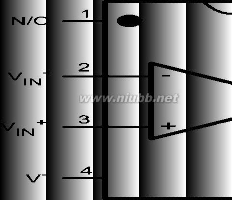
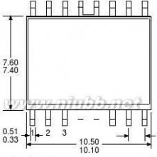
Connection Diagrams
5-Pin SOT23
8-Pin SOIC
Top View
30033802
Top View
30033842
Ordering Information
Package
Part NumberLMP2231AMFLMP2231AMFE
5-Pin SOT23
LMP2231AMFXLMP2231BMFLMP2231BMFELMP2231BMFXLMP2231AMALMP2231AMAE
8-Pin SOIC
LMP2231AMAXLMP2231BMALMP2231BMAELMP2231BMAX
LMP2231BMA
?40°C to 125°C
LMP2231AMA
AL5BAL5A
Temperature
Range
Package Marking
Transport Media1k Units Tape and Reel250 Units Tape and Reel3k Units Tape and Reel1k Units Tape and Reel250 Units Tape and Reel3k Units Tape and Reel
95 Units/Rail250 Units Tape and Reel2.5k Units Tape and Reel
95 Units/Rail250 Units Tape and Reel2.5k Units Tape and Reel
M08AMF05ANSC Drawing
www.national.com6
2231 LMP2231中文资料
扩展:lmp2231 / 2231均衡器中文说明书 / lmp91000中文手册
元器件交易网www.cecb2b.com
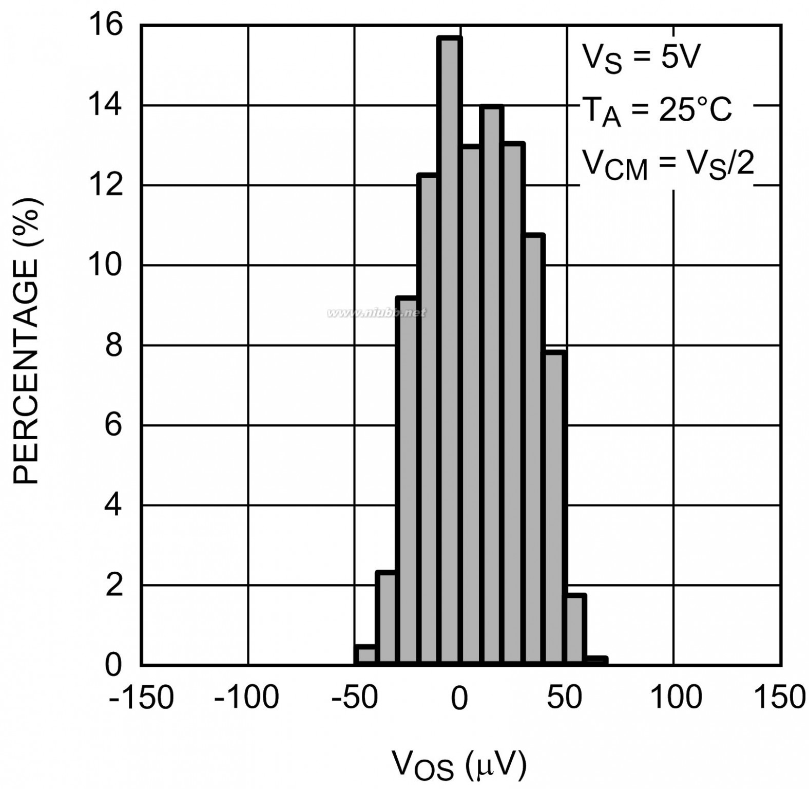
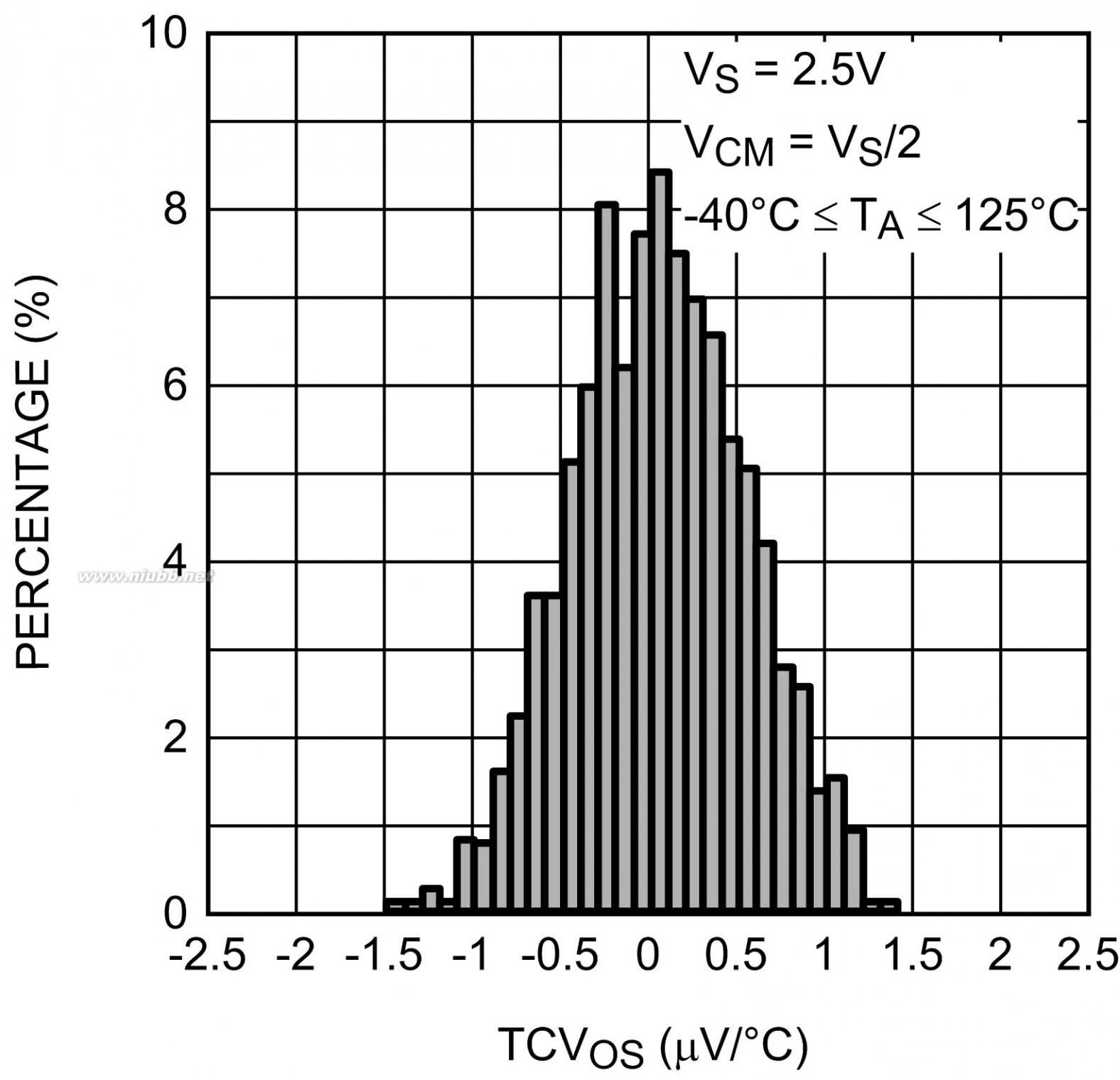
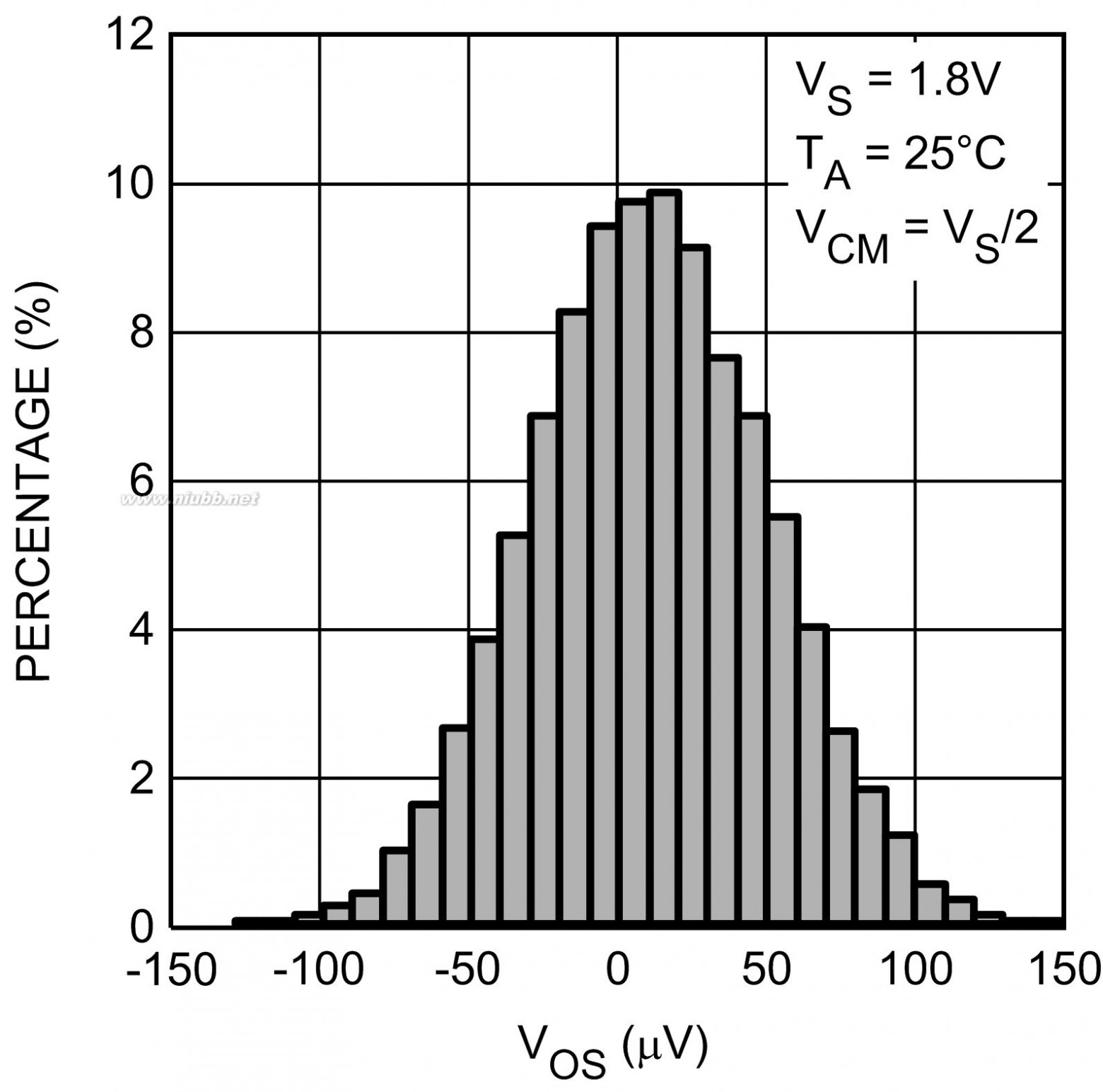
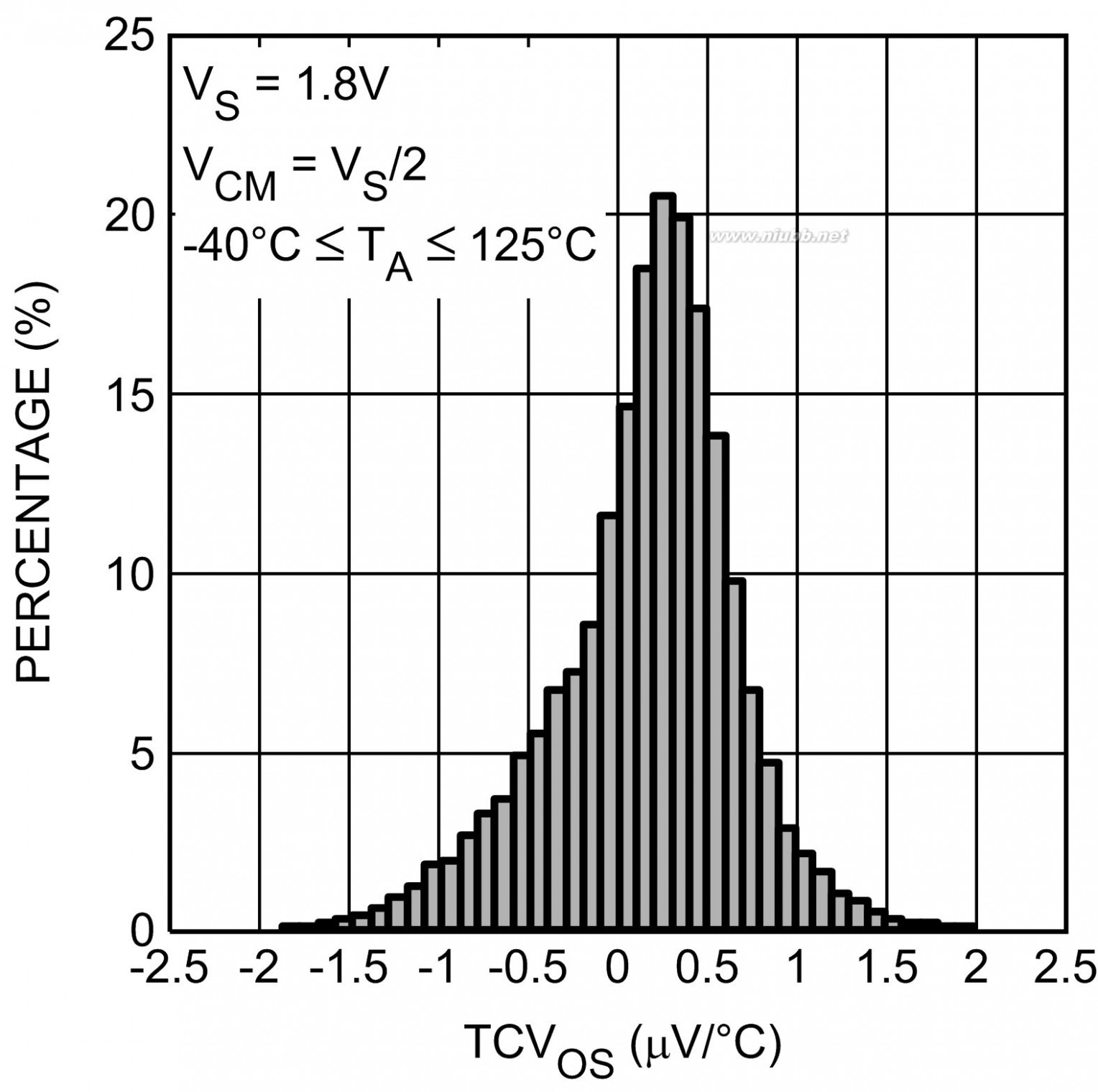
LMP2231 SingleTypical Performance Characteristics
VS = V+ - V?
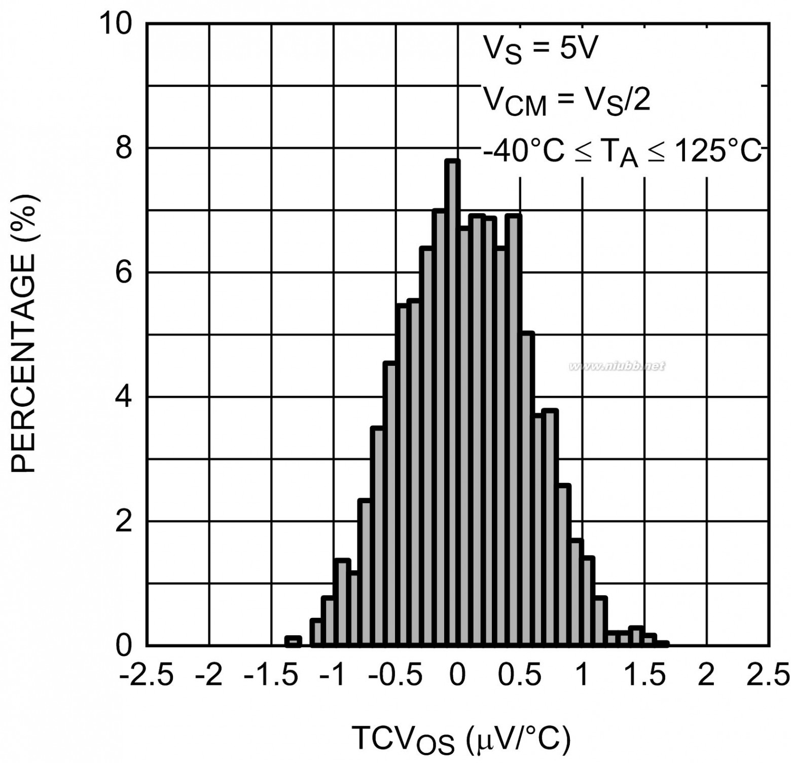
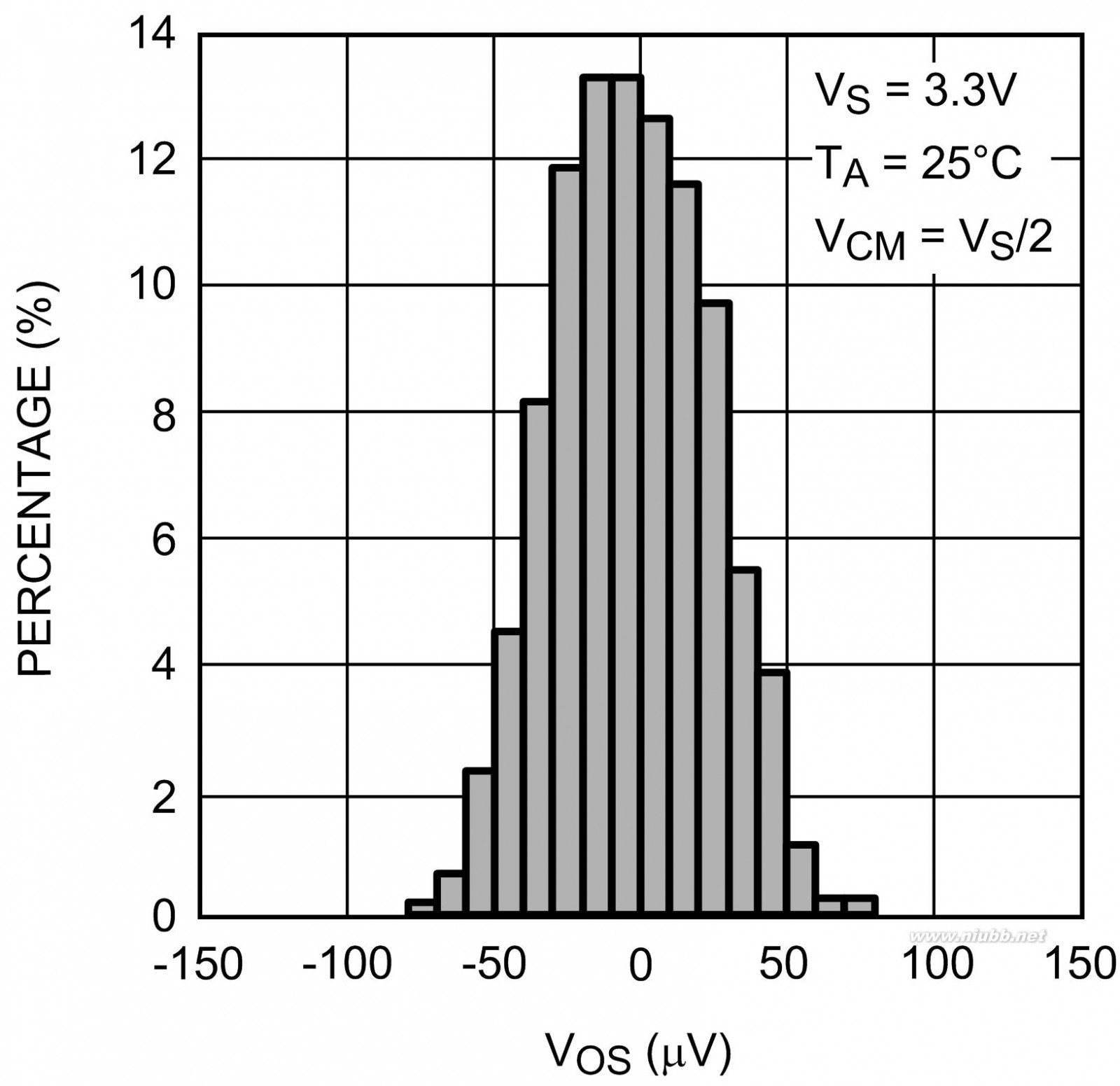
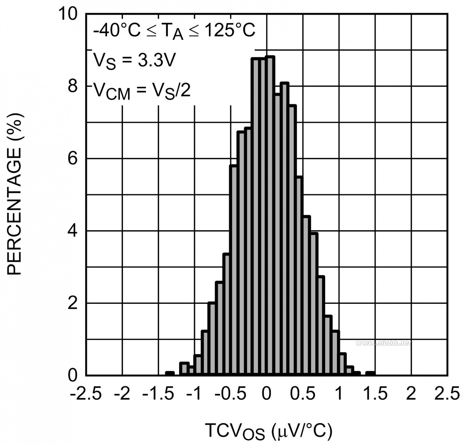
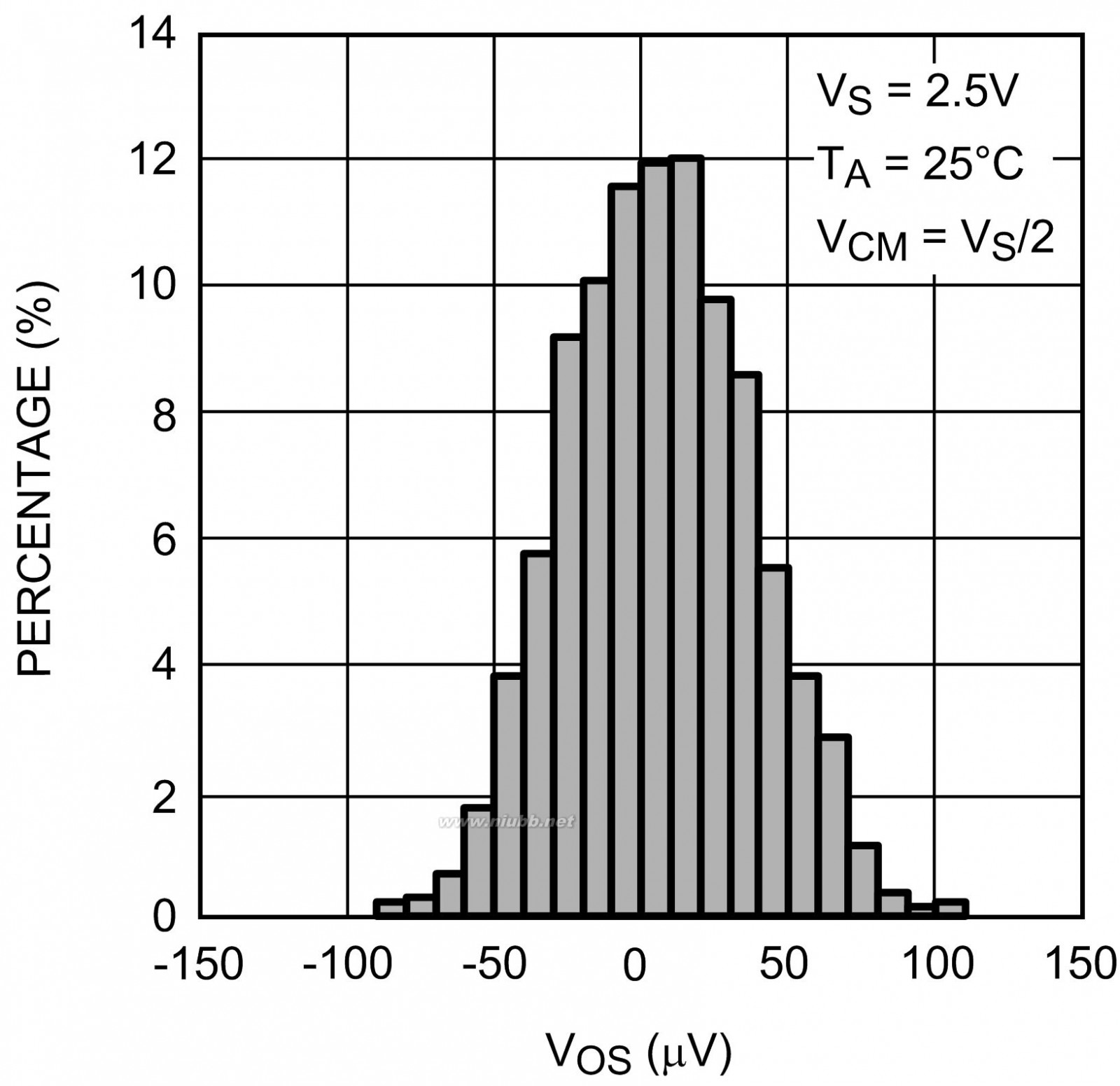
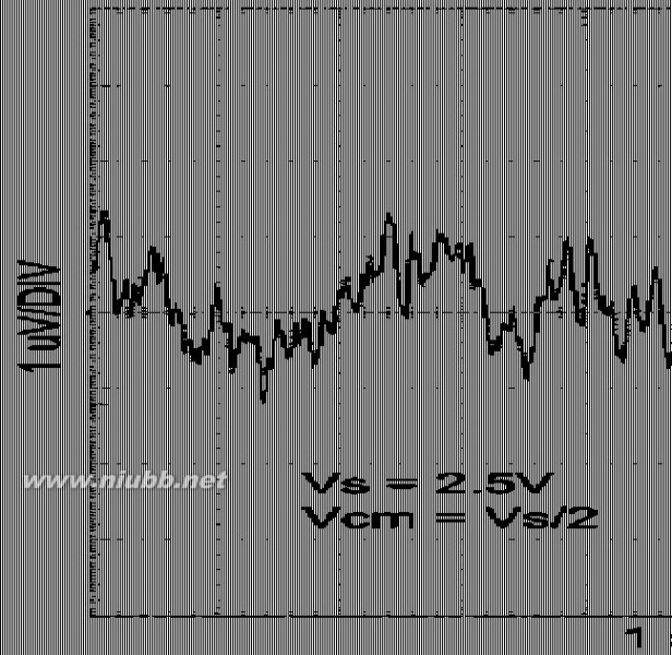
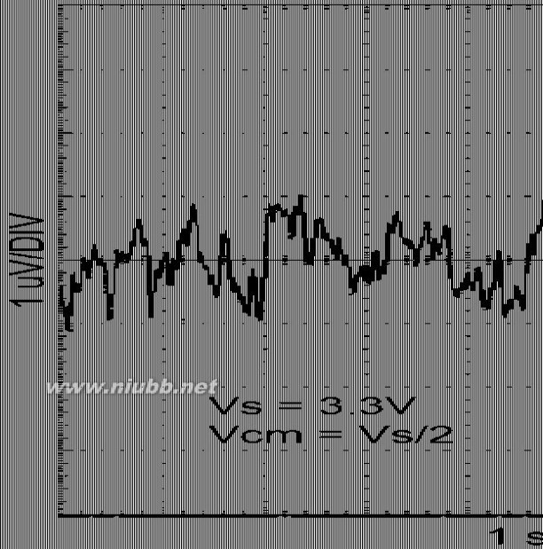
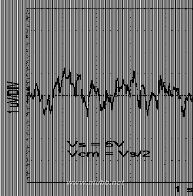
Offset Voltage DistributionUnless otherwise Specified: TA = 25°C, VS = 5V, VCM = VS/2, whereTCVOS Distribution
3003380730033811
Offset Voltage DistributionTCVOS Distribution
3003380630033810
Offset Voltage DistributionTCVOS Distribution
3003380530033809
7www.national.com
2231 LMP2231中文资料

元器件交易网www.cecb2b.com
LMP2231 SingleOffset Voltage DistributionTCVOS Distribution
3003387330033869
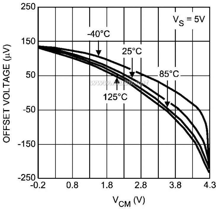
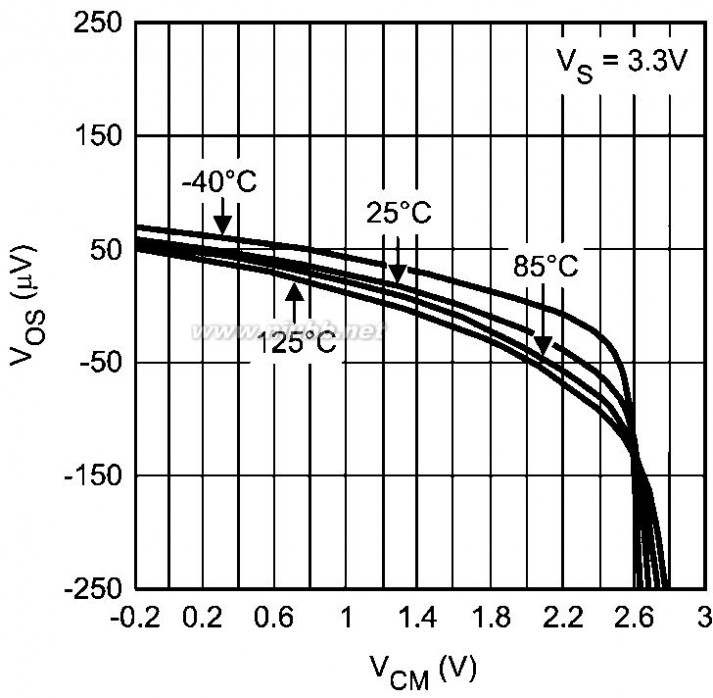
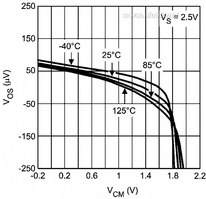
Offset Voltage vs. VCMOffset Voltage vs. VCM
3003381830033865
Offset Voltage vs. VCMOffset Voltage vs. VCM
3003386430033872
www.national.com8
2231 LMP2231中文资料

元器件交易网www.cecb2b.com
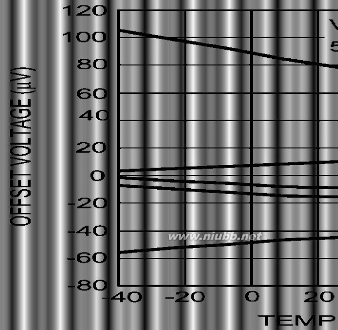
LMP2231 SingleOffset Voltage vs. TemperatureOffset Voltage vs. Supply Voltage
3003387130033870
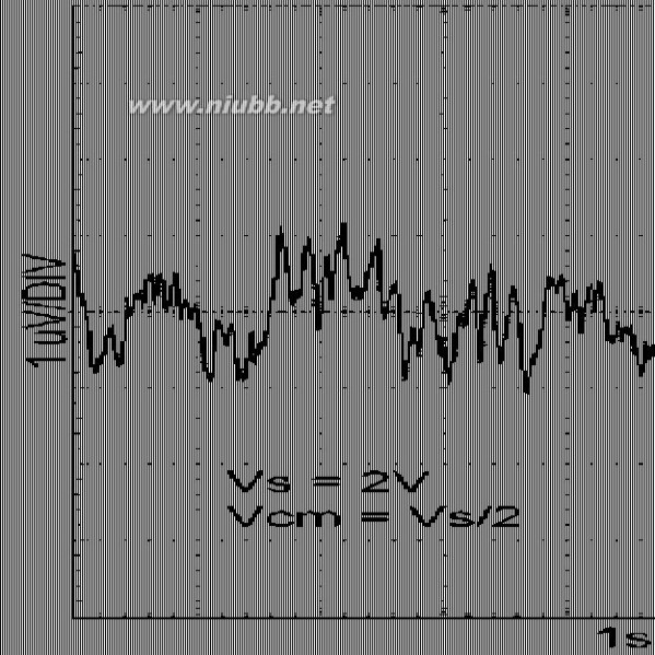
Time Domain Voltage NoiseTime Domain Voltage Noise
3003383330033834
Time Domain Voltage NoiseTime Domain Voltage Noise
30033832
30033831
9www.national.com
2231 LMP2231中文资料
元器件交易网www.cecb2b.com
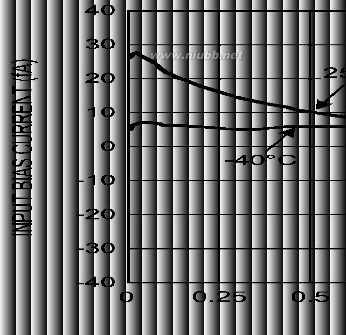
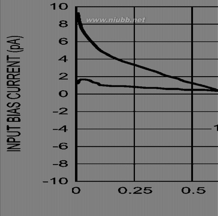
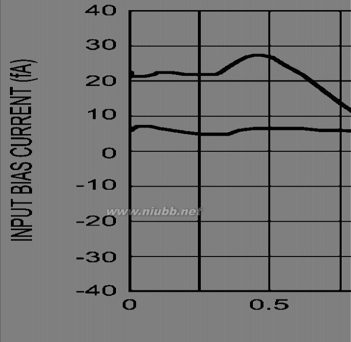
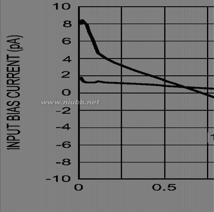
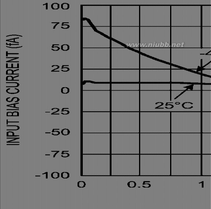
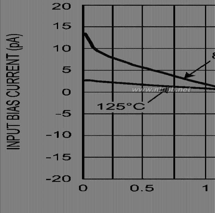
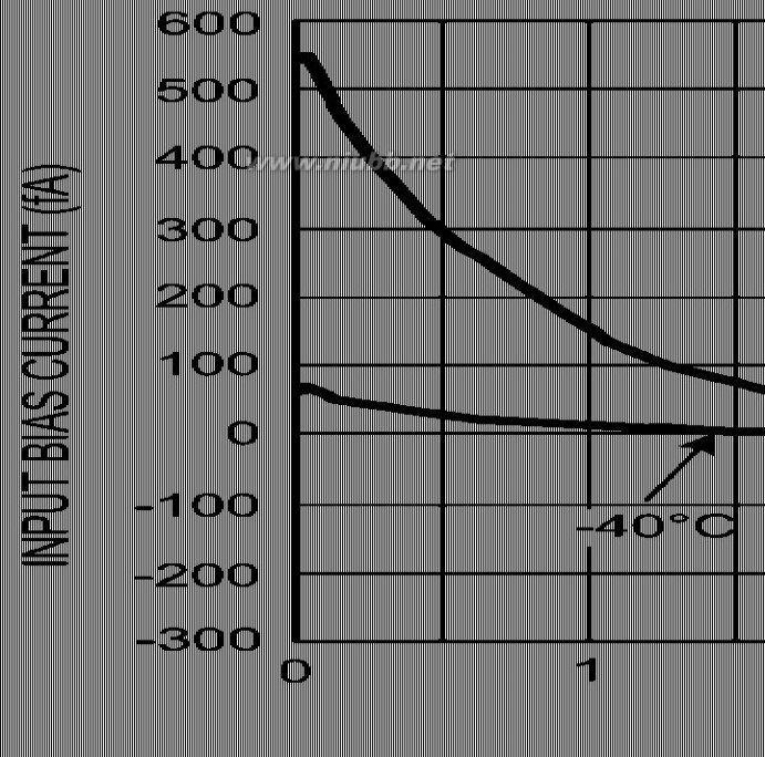
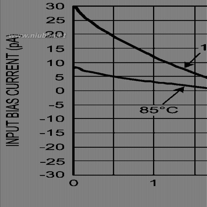
LMP2231 SingleInput Bias Current vs. VCMInput Bias Current vs. VCM
3003385530033856
Input Bias Current vs. VCMInput Bias Current vs. VCM
3003385730033858
Input Bias Current vs. VCMInput Bias Current vs. VCM
3003385930033860
www.national.com10
2231 LMP2231中文资料
元器件交易网www.cecb2b.com
LMP2231 SingleInput Bias Current vs. VCMInput Bias Current vs. VCM
3003386130033862
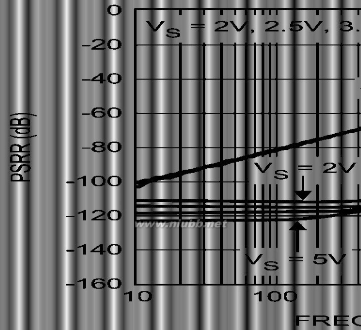
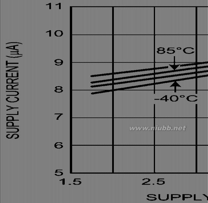
PSRR vs. FrequencySupply Current vs. Supply Voltage
3003386630033812
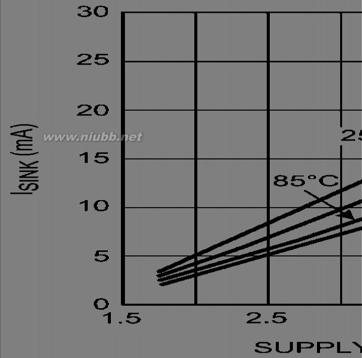
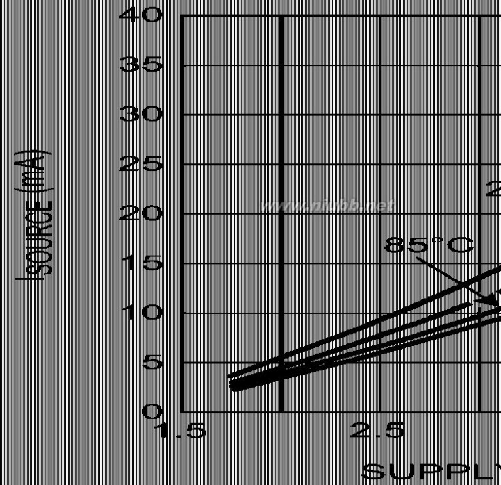
Sinking Current vs. Supply VoltageSourcing Current vs. Supply Voltage
3003381330033814
11www.national.com
2231 LMP2231中文资料
扩展:lmp2231 / 2231均衡器中文说明书 / lmp91000中文手册
元器件交易网www.cecb2b.com
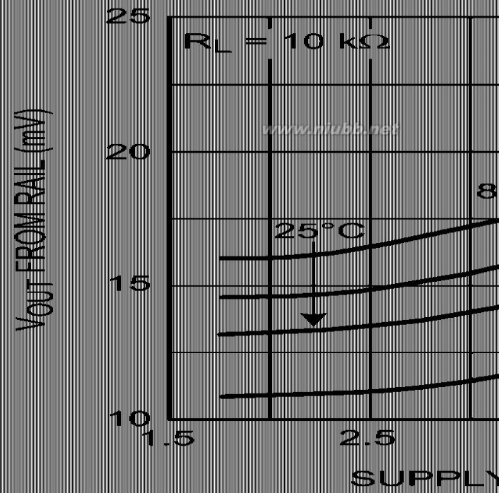
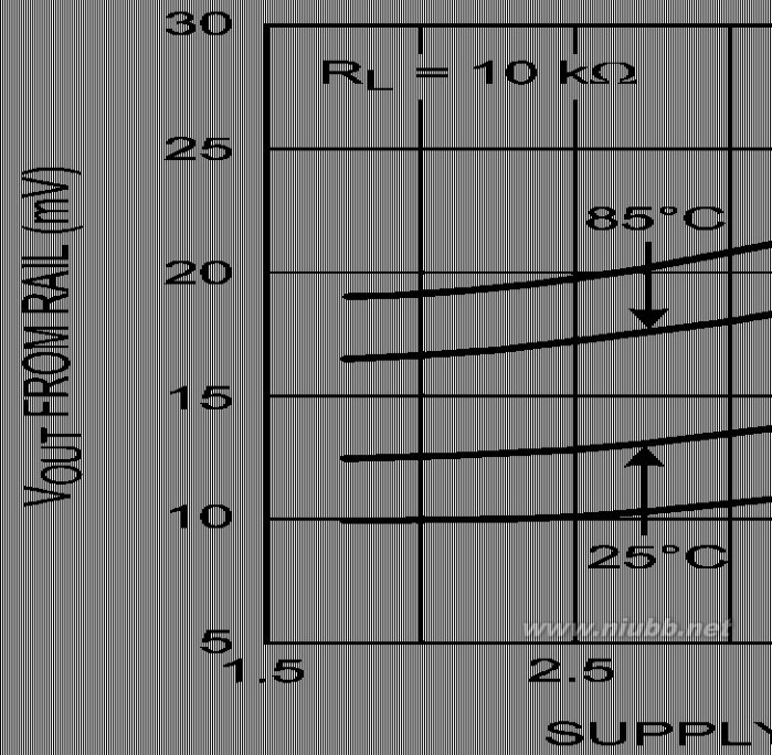
LMP2231 SingleOutput Swing High vs. Supply VoltageOutput Swing Low vs. Supply Voltage
3003381530033816
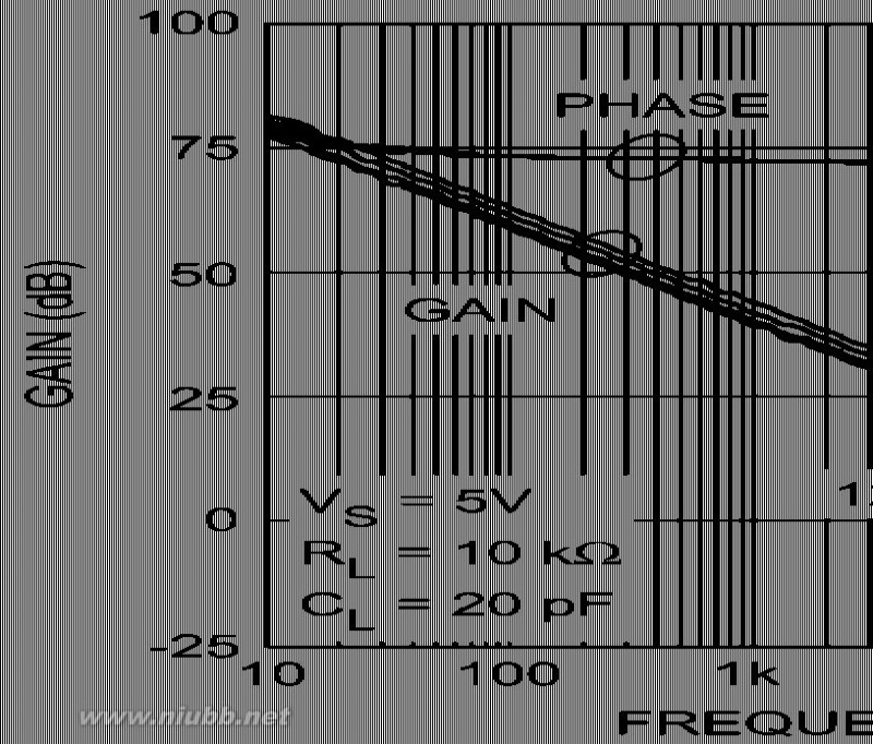
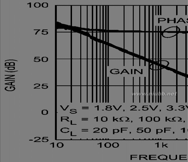
Open Loop Frequency ResponseOpen Loop Frequency Response
3003382130033822
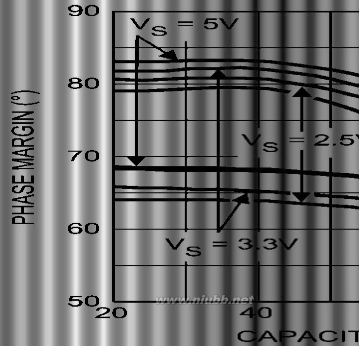
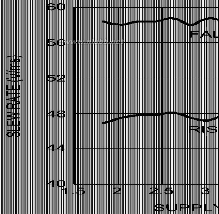
Phase Margin vs. Capacitive LoadSlew Rate vs. Supply Voltage
3003386330033830
www.national.com12
2231 LMP2231中文资料
元器件交易网www.cecb2b.com
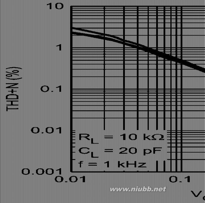
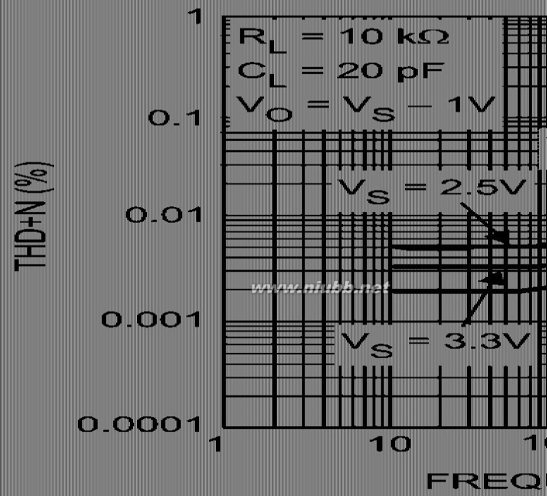
LMP2231 SingleTHD+N vs. AmplitudeTHD+N vs. Frequency
3003382830033829
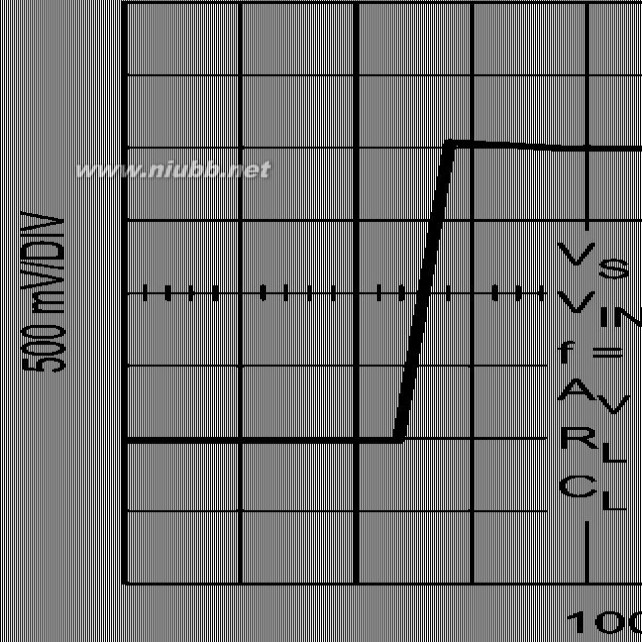
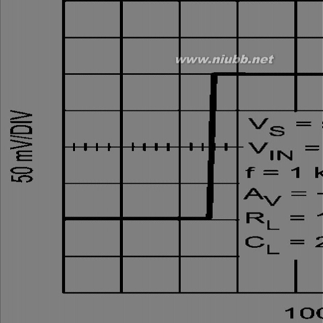
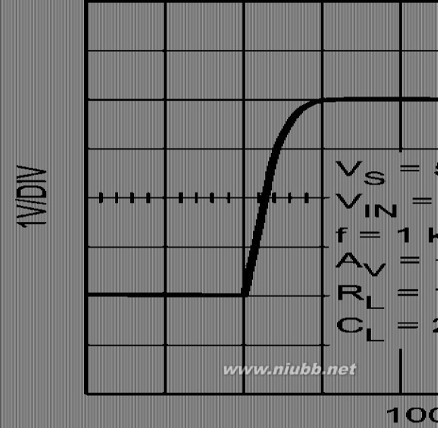
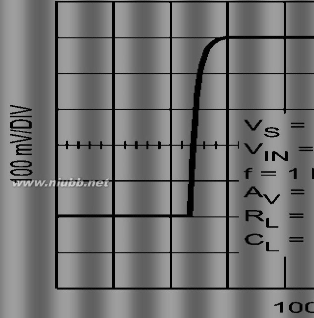
Large Signal Step ResponseSmall Signal Step Response
3003382430033823
Large Signal Step ResponseSmall Signal Step Response
3003382630033825
13www.national.com
2231 LMP2231中文资料
元器件交易网www.cecb2b.com
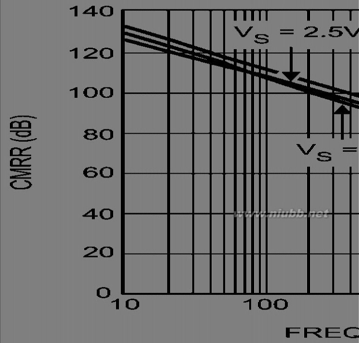
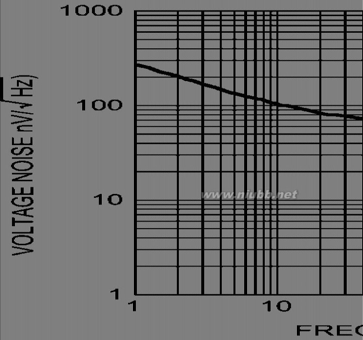
LMP2231 SingleCMRR vs. FrequencyInput Voltage Noise vs. Frequency
3003386730033819
www.national.com14
2231 LMP2231中文资料


元器件交易网www.cecb2b.com
LMP2231 SingleApplication Information
LMP2231
The LMP2231 is a single CMOS precision amplifier that offerlow offset voltage and low offset voltage drift, and high gainwhile only consuming 10 μA of current per channel.
The LMP2231 is a micropower op amp, consuming only10 μA of current. Micropower op amps extend the run time ofbattery powered systems and reduce energy consumption inenergy limited systems. The guaranteed supply voltage rangeof 1.8V to 5.0V along with the ultra-low supply current extendthe battery run time in two ways. The extended guaranteedpower supply voltage range of 1.8V to 5.0V enables the opamp to function when the battery voltage has depleted fromits nominal value down to 1.8V. In addition, the lower powerconsumption increases the life of the battery.
The LMP2231 has an input referred offset voltage of only±150 μV maximum at room temperature. This offset is guar-anteed to be less than ±230 μV over temperature. This mini-mal offset voltage along with very low TCVOS of only0.3 μV/°C typical allows more accurate signal detection andamplification in precision applications.
The low input bias current of only ±20 fA gives the LMP2231superiority for use in high impedance sensor applications.Bias Current of an amplifier flows through source resistanceof the sensor and the voltage resulting from this current flowappears as a noise voltage on the input of the amplifier. Thelow input bias current enables the LMP2231 to interface withhigh impedance sensors while generating negligible voltagenoise. Thus the LMP2231 provides better signal fidelity anda higher signal-to-noise ration when interfacing with highimpedance sensors.
National Semiconductor is heavily committed to precisionamplifiers and the market segment they serve. Technical sup-port and extensive characterization data is available for sen-sitive applications or applications with a constrained errorbudget.
The operating supply voltage range of 1.8V to 5.5V over theextensive temperature range of ?40°C to 125°C makes theLMP2231 an excellent choice for low voltage precision appli-cations with extensive temperature requirements.
The LMP2231 is offered in the space saving 5-Pin SOT23 and8-pin SOIC package. These small packages are ideal solu-tions for area constrained PC boards and portable electron-ics.
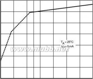
TOTAL NOISE CONTRIBUTION
The LMP2231 has a very low input bias current, very low inputcurrent noise, and low input voltage noise for micropoweramplifier. As a result, this amplifier makes a great choice forcircuits with high impedance sensor applications.
Figure 1 shows the typical input noise of the LMP2231 as afunction of source resistance where:
扩展:lmp2231 / 2231均衡器中文说明书 / lmp91000中文手册
en denotes the input referred voltage noise
ei is the voltage drop across source resistance due to inputreferred current noise or ei = RS * in
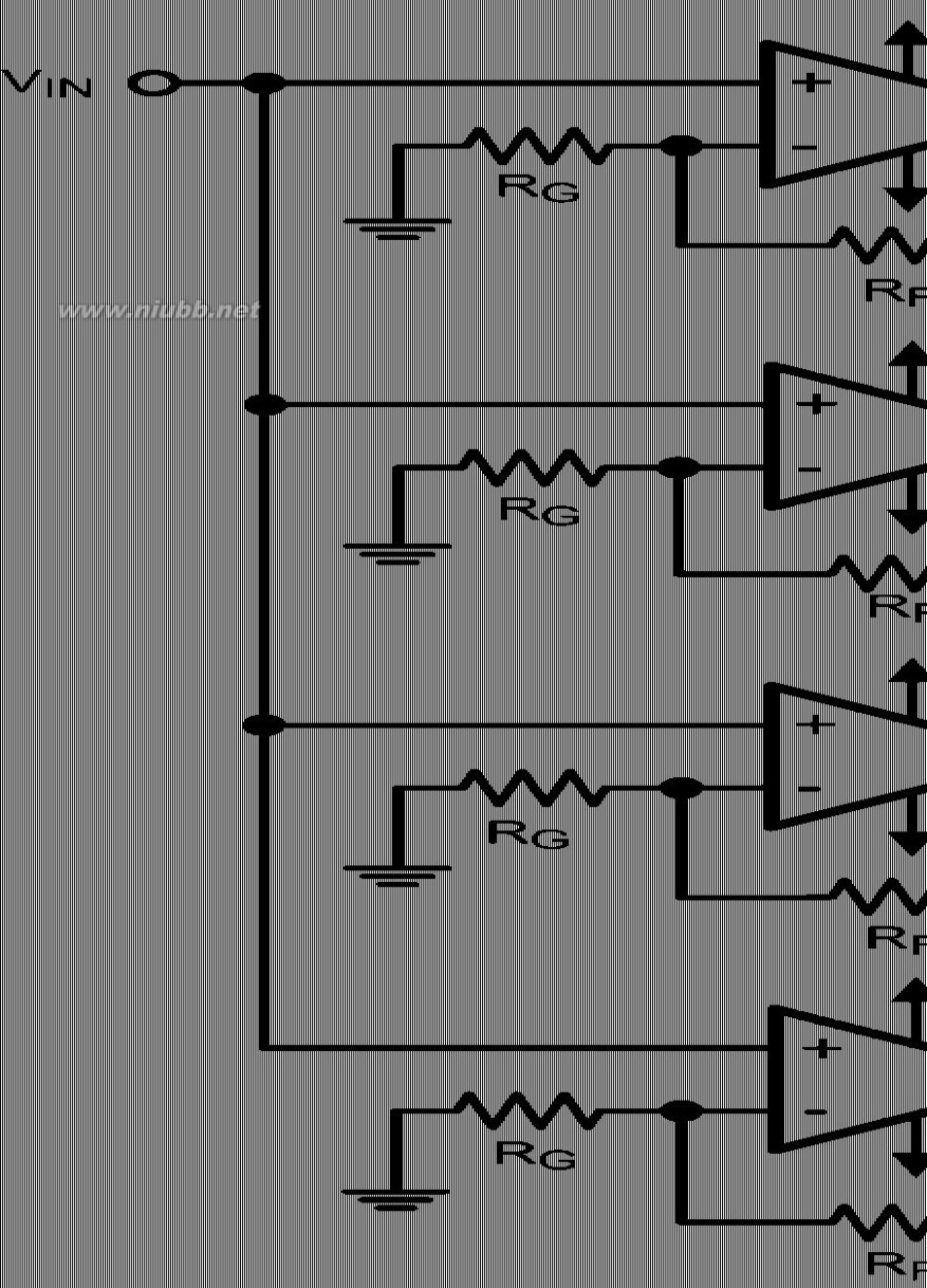
et shows the thermal noise of the source resistanceeni shows the total noise on the input.Where:The input current noise of the LMP2231 is so low that it willnot become the dominant factor in the total noise unlesssource resistance exceeds 300 M?, which is an unrealisti-cally high value. As is evident in Figure 1, at lower RS values,total noise is dominated by the amplifier’s input voltage noise.Once RS is larger than a 100 k?, then the dominant noisefactor becomes the thermal noise of RS. As mentioned before,the current noise will not be the dominant noise factor for anypractical application.30033848FIGURE 1. Total Input NoiseVOLTAGE NOISE REDUCTION . WhileThe LMP2231 has an input voltage noise of 60 nV/this value is very low for micropower amplifiers, this inputvoltage noise can be further reduced by placing N amplifiersin parallel as shown in Figure 2. The total voltage noise on theoutput of this circuit is divided by the square root of the num-ber of amplifiers used in this parallel combination. This isbecause each individual amplifier acts as an independentnoise source, and the average noise of independent sourcesis the quadrature sum of the independent sources divided bythe number of sources. For N identical amplifiers, this means:
15www.national.com
2231 LMP2231中文资料


元器件交易网www.cecb2b.com
LMP2231 Single
Figure 2 shows a schematic of this input voltage noise reduc-tion circuit. Typical resistor values are: RG = 10?, RF = 1 k?,and RO = 1 k?.
30033836
FIGURE 3. Instrumentation Amplifier
There are two stages in this amplifier. The last stage, outputstage, is a differential amplifier. In an ideal case the two am-plifiers of the first stage, input stage, would be set up asbuffers to isolate the inputs. However they cannot be con-nected as followers because of mismatch of amplifiers. Thatis why there is a balancing resistor between the two. Theproduct of the two stages of gain will give the gain of the in-strumentation amplifier. Ideally, the CMRR should be infinite.However the output stage has a small non-zero commonmode gain which results from resistor mismatch.
In the input stage of the circuit, current is the same across allresistors. This is due to the high input impedance and lowinput bias current of the LMP2231.
30033846
(1)
By Ohm’s Law:
FIGURE 2. Noise Reduction Circuit
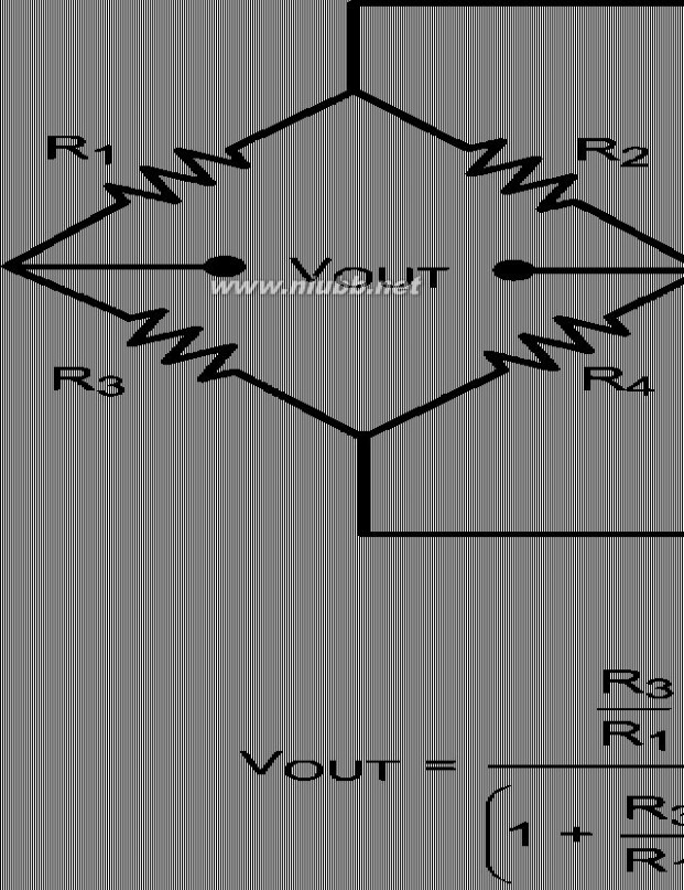
PRECISION INSTRUMENTATION AMPLIFIER
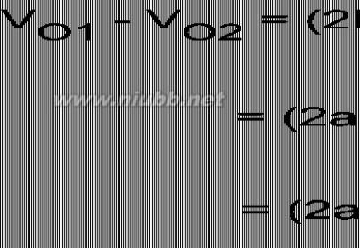
Measurement of very small signals with an amplifier requiresclose attention to the input impedance of the amplifier, gainof the overall signal on the inputs, and the gain on each inputof the amplifier. This is because the difference of the inputsignal on the two inputs is of the interest and the commonsignal is considered noise. A classic circuit implementation isan instrumentation amplifier. Instrumentation amplifiers havea finite, accurate, and stable gain. They also have extremelyhigh input impedances and very low output impedances. Fi-nally they have an extremely high CMRR so that the amplifiercan only respond to the differential signal. A typical instru-mentation amplifier is shown in Figure 3.
(2)
However:
(3)
So we have:
VO1–VO2 = (2a+1)(V1–V2)
(4)
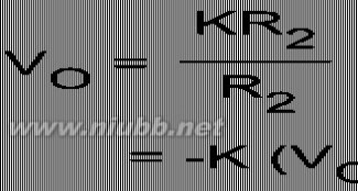
Now looking at the output of the instrumentation amplifier:
(5)
Substituting from Equation 4:
(6)
This shows the gain of the instrumentation amplifier to be:
?K(2a+1)
Typical values for this circuit can be obtained by setting:a = 12 and K= 4. This results in an overall gain of ?100.
www.national.com16
2231 LMP2231中文资料
元器件交易网www.cecb2b.com
LMP2231 SingleSINGLE SUPPLY STRAIN GAGE BRIDGE AMPLIFIER
Strain gauges are popular electrical elements used to mea-sure force or pressure. Strain gauges are subjected to anunknown force which is measured as a the deflection on apreviously calibrated scale. Pressure is often measured usingthe same technique; however this pressure needs to be con-verted into force using an appropriate transducer. Straingauges are often resistors which are sensitive to pressure orto flexing. Sense resistor values range from tens of ohms toseveral hundred kilo ohms. The resistance change which is aresult of applied force across the strain gauge might be 1% ofits total value. An accurate and reliable system is needed tomeasure this small resistance change. Bridge configurationsoffer a reliable method for this measurement.
扩展:lmp2231 / 2231均衡器中文说明书 / lmp91000中文手册
Bridge sensors are formed of four resistors, connected as aquadrilateral. A voltage source or a current source is usedacross one of the diagonals to excite the bridge while a volt-age detector across the other diagonal measures the outputvoltage.
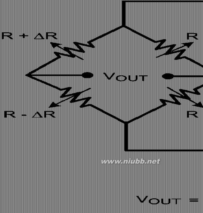
Bridges are mainly used as null circuits or to measure a dif-ferential voltages. Bridges will have no output voltage if theratios of two adjacent resistor values are equal. This fact isused in null circuit measurements. These are particularlyused in feedback systems which involve electrochemical el-ements or human interfaces. Null systems force an activeresistor, such as a strain gauge, to balance the bridge by in-fluencing the measured parameter.Often in sensor applications at lease one of the resistors is avariable resistor, or a sensor. The deviation of this active el-ement from its initial value is measured as an indication ofchange in the measured quantity. A change in output voltagerepresents the sensor value change. Since the sensor valuechange is often very small, the resulting output voltage is verysmall in magnitude as well. This requires an extensive andvery precise amplification circuitry so that signal fidelity doesnot change after amplification.Sensitivity of a bridge is the ratio of its maximum expectedoutput change to the excitation voltage change.Figure 4 (a) shows a typical bridge sensor and Figure 4(b)shows the bridge with four sensors. R in Figure 4(b) is thenominal value of the sense resistor and the deviations from Rare proportional to the quantity being measured.
30033851
30033850FIGURE 4. Bridge Sensor
ence. The other three LMP2231s are used to form an instru-mentation amplifier. This instrumentation amplifier uses theLMP2231's high CMRR and low VOS and TCVOS to accuratelyamplify the small differential signal generated by the output ofthe bridge sensor. This amplified signal is then fed into theADC121S021 which is a 12-bit analog to digital converter.This circuit works on a single supply voltage of 5V.Instrumentation amplifiers are great for interfacing with bridgesensors. Bridge sensors often sense a very small differentialsignal in the presence of a larger common mode voltage. In-strumentation amplifiers reject this common mode signal.Figure 5 shows a strain gauge bridge amplifier. In this appli-cation the LMP2231 is used to buffer the LM4140's precision
output voltage. The LM4140A is a precision voltage refer-
17www.national.com
2231 LMP2231中文资料
元器件交易网www.cecb2b.com
LMP2231 Single
30033874
FIGURE 5. Strain Gauge Bridge Amplifier
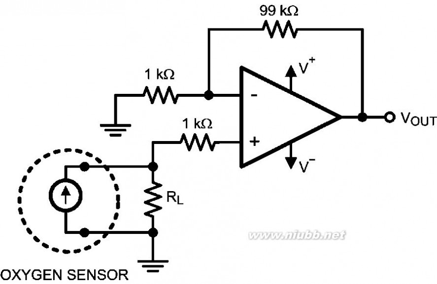
PORTABLE GAS DETECTION SENSOR
Gas sensors are used in many different industrial and medicalapplications. They generate a current which is proportional tothe percentage of a particular gas sensed in an air sample.This current goes through a load resistor and the resultingvoltage drop is measured. Depending on the sensed gas andsensitivity of the sensor, the output current can be in the orderof tens of microamperes to a few milliamperes. Gas sensordatasheets often specify a recommended load resistor valueor they suggest a range of load resistors to choose from.Oxygen sensors are used when air quality or oxygen deliv-ered to a patient needs to be monitored. Fresh air contains20.9% oxygen. Air samples containing less than 18% oxygenare considered dangerous. Oxygen sensors are also used inindustrial applications where the environment must lack oxy-gen. An example is when food is vacuum packed. There aretwo main categories of oxygen sensors, those which senseoxygen when it is abundantly present (i.e. in air or near anoxygen tank) and those which detect traces of oxygen in ppm.Figure 6 shows a typical circuit used to amplify the output ofan oxygen detector. The LMP2231 makes an excellent choicefor this application as it only draws 10 μA of current and op-erates on supply voltages down to 1.8V. This applicationdetects oxygen in air. The oxygen sensor outputs a knowncurrent through the load resistor. This value changes with theamount of oxygen present in the air sample. Oxygen sensorsusually recommend a particular load resistor value or specifya range of acceptable values for the load resistor. Oxygensensors typically have a life of one to two years. The use ofthe micropower LMP2231 means minimal power usage by theop amp and it enhances the battery life. Depending on othercomponents present in the circuit design, the battery couldlast for the entire life of the oxygen sensor. The precisionspecifications of the LMP2231, such as its very low offsetvoltage, low TCVOS , low input bias current, low CMRR, andlow PSRR are other factors which make the LMP2231 a greatchoice for this application.30033849FIGURE 6. Precision Oxygen Sensor
www.national.com18
2231 LMP2231中文资料
扩展:lmp2231 / 2231均衡器中文说明书 / lmp91000中文手册
元器件交易网www.cecb2b.com
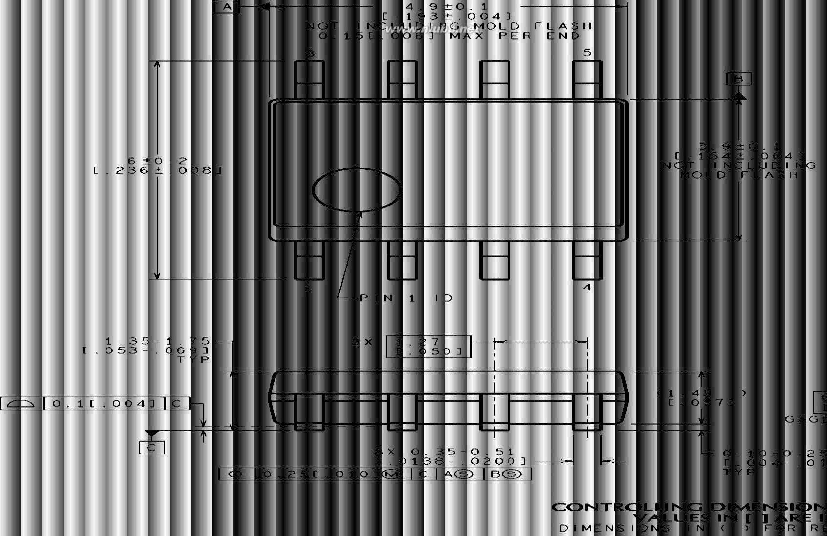
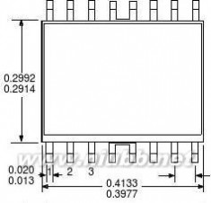
LMP2231 SinglePhysical Dimensions inches (millimeters) unless otherwise noted
5-Pin SOT23
NS Package Number MF0A5
8-Pin SOIC
NS Package Number M08A
19www.national.com
2231 LMP2231中文资料
元器件交易网www.cecb2b.com
LMP2231 Single Micropower, 1.8V, Precision, Operational Amplifier with CMOS Inputs
Notes

For more National Semiconductor product information and proven design tools, visit the following Web sites at:
Products
AmplifiersAudio
Clock ConditionersData ConvertersDisplaysEthernetInterfaceLVDS
Power Management Switching Regulators LDOs LED LightingPowerWise
Serial Digital Interface (SDI)Temperature SensorsWireless (PLL/VCO)
www.national.com/amplifierswww.national.com/audiowww.national.com/timingwww.national.com/adcwww.national.com/displayswww.national.com/ethernetwww.national.com/interfacewww.national.com/lvdswww.national.com/powerwww.national.com/switcherswww.national.com/ldowww.national.com/ledwww.national.com/powerwisewww.national.com/sdi
www.national.com/tempsensorswww.national.com/wireless
WEBENCHAnalog UniversityApp NotesDistributorsGreen CompliancePackaging
Design Support
www.national.com/webenchwww.national.com/AUwww.national.com/appnoteswww.national.com/contactswww.national.com/quality/greenwww.national.com/packagingwww.national.com/qualitywww.national.com/refdesignswww.national.com/feedback
Quality and ReliabilityReference DesignsFeedback
THE CONTENTS OF THIS DOCUMENT ARE PROVIDED IN CONNECTION WITH NATIONAL SEMICONDUCTOR CORPORATION(“NATIONAL”) PRODUCTS. NATIONAL MAKES NO REPRESENTATIONS OR WARRANTIES WITH RESPECT TO THE ACCURACYOR COMPLETENESS OF THE CONTENTS OF THIS PUBLICATION AND RESERVES THE RIGHT TO MAKE CHANGES TOSPECIFICATIONS AND PRODUCT DESCRIPTIONS AT ANY TIME WITHOUT NOTICE. NO LICENSE, WHETHER EXPRESS,IMPLIED, ARISING BY ESTOPPEL OR OTHERWISE, TO ANY INTELLECTUAL PROPERTY RIGHTS IS GRANTED BY THISDOCUMENT.
TESTING AND OTHER QUALITY CONTROLS ARE USED TO THE EXTENT NATIONAL DEEMS NECESSARY TO SUPPORTNATIONAL’S PRODUCT WARRANTY. EXCEPT WHERE MANDATED BY GOVERNMENT REQUIREMENTS, TESTING OF ALLPARAMETERS OF EACH PRODUCT IS NOT NECESSARILY PERFORMED. NATIONAL ASSUMES NO LIABILITY FORAPPLICATIONS ASSISTANCE OR BUYER PRODUCT DESIGN. BUYERS ARE RESPONSIBLE FOR THEIR PRODUCTS ANDAPPLICATIONS USING NATIONAL COMPONENTS. PRIOR TO USING OR DISTRIBUTING ANY PRODUCTS THAT INCLUDENATIONAL COMPONENTS, BUYERS SHOULD PROVIDE ADEQUATE DESIGN, TESTING AND OPERATING SAFEGUARDS.
EXCEPT AS PROVIDED IN NATIONAL’S TERMS AND CONDITIONS OF SALE FOR SUCH PRODUCTS, NATIONAL ASSUMES NOLIABILITY WHATSOEVER, AND NATIONAL DISCLAIMS ANY EXPRESS OR IMPLIED WARRANTY RELATING TO THE SALEAND/OR USE OF NATIONAL PRODUCTS INCLUDING LIABILITY OR WARRANTIES RELATING TO FITNESS FOR A PARTICULARPURPOSE, MERCHANTABILITY, OR INFRINGEMENT OF ANY PATENT, COPYRIGHT OR OTHER INTELLECTUAL PROPERTYRIGHT.
LIFE SUPPORT POLICY
NATIONAL’S PRODUCTS ARE NOT AUTHORIZED FOR USE AS CRITICAL COMPONENTS IN LIFE SUPPORT DEVICES ORSYSTEMS WITHOUT THE EXPRESS PRIOR WRITTEN APPROVAL OF THE CHIEF EXECUTIVE OFFICER AND GENERALCOUNSEL OF NATIONAL SEMICONDUCTOR CORPORATION. As used herein:
Life support devices or systems are devices which (a) are intended for surgical implant into the body, or (b) support or sustain life andwhose failure to perform when properly used in accordance with instructions for use provided in the labeling can be reasonably expectedto result in a significant injury to the user. A critical component is any component in a life support device or system whose failure to performcan be reasonably expected to cause the failure of the life support device or system or to affect its safety or effectiveness.
National Semiconductor and the National Semiconductor logo are registered trademarks of National Semiconductor Corporation. All otherbrand or product names may be trademarks or registered trademarks of their respective holders.
Copyright? 2008 National Semiconductor Corporation
For the most current product information visit us at www.national.com
National SemiconductorAmericas TechnicalSupport CenterEmail:
new.feedback@nsc.comTel: 1-800-272-9959
www.national.com
National Semiconductor EuropeTechnical Support Center
Email: europe.support@nsc.comGerman Tel: +49 (0) 180 5010 771English Tel: +44 (0) 870 850 4288
National Semiconductor AsiaPacific Technical Support CenterEmail: ap.support@nsc.com
National Semiconductor JapanTechnical Support CenterEmail: jpn.feedback@nsc.com
扩展:lmp2231 / 2231均衡器中文说明书 / lmp91000中文手册
三 : A8181中文资料
元器件交易网www.cecb2b.com
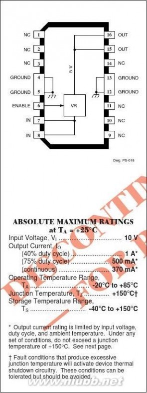
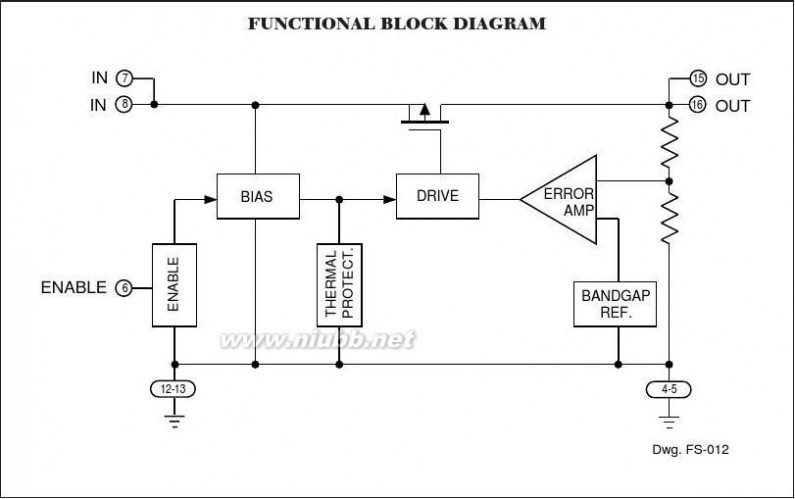
8181LOW-DROPOUT,5 V REGULATOR
8181
LOW-DROPOUT, 5 V REGULATOR— HIGH EFFICIENCY
Especially suited for hand-held, portable, battery-operated equip-ment such as cellular telephones, the A8181SLB low dropout voltageregulator provides high efficiency for maximum battery life in a mini-mum package size. Equally applicable to camcorders and portablecomputers, the device provides a fixed 5 V regulated continuous outputat almost 200 mA of load current under worst-case conditions. Undernormal operating conditions, output currents over 500 mA are
permitted.
A MOSFET pass element delivers high output current with an
input-output differential of less than 300 mV. For high efficiency, thelow dropout voltage allows a longer battery discharge before outputvoltage regulation is lost. A low quiescent current, even during highload conditions, makes the device ideal for standby power systems.High regulator accuracy and excellent temperature characteristics areprovided by a bandgap reference. An enable input gives the designercomplete control over sequential power-up or emergency shutdown.
This device is supplied in a 16-lead wide-body, small-outline
plastic power package (SOIC) for surface-mount applications. Thecopper batwing provides for maximum package power dissipation inthe smallest possible construction. The A8181SLB is rated for opera-tion over a temperature range of -20°C to +85°C.Data Sheet27468*TCUYDLONRO PEDCENUEREFEFEATURES AND BENEFITSsssss

High Efficiency Provides Extended Battery LifeLess Than 300 mV Dropout VoltageLow Quiescent Current>200 mA Output CurrentLSTTL-Compatible ON/OFF ControlFor Sequential Power-up or Emergency ShutdownsInternal Thermal ProtectionsSOIC Surface-Mount Package
Always order by complete part number:A8181SLB.
8181 A8181中文资料
元器件交易网www.cecb2b.com
8181
LOW-DROPOUT,

5 V REGULATOR
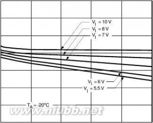
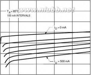
MAXIMUM ALLOWABLE OUTPUT CURRENT with device mounted on 2.24" x 2.24"(56.9 mm x 56.9 mm) solder-coated copper-clad board in still air.
Maximum Allowable Output Current in Milliamperes with VI = 10 V, TJ = 150°C*
dc (Duty Cycle)
TA25°C50°C70°C85°C
100%370295235190
90%415330265215
80%465370295240
70%530425340275
60%620495395320
50%745595475385
40%930745595485
30%1000995795645
20%100010001000970
*IO = (TJ - TA)/([VI - VO] RθJA ? dc) = (150 - TA)/(5 ? 67 ? dc)
Output current rating can be increased (to 1 A maximum) by heat sinking or reducing the input voltage. With an infinite heat sink, R-JA = R-JT =6°C/W. Conditions that produce excessive junction temperature will activate device thermal shutdown circuitry. These conditions can be toleratedbut should be avoided.
115 Northeast Cutoff, Box 15036
Worcester, Massachusetts 01615-0036 (508) 853-5000
W
Copyright ? 1992, 1995 Allegro MicroSystems, Inc.
8181 A8181中文资料
元器件交易网www.cecb2b.com
8181
LOW-DROPOUT,5 V REGULATOR
ELECTRICAL CHARACTERISTICS at TA +25°C (unless otherwise noted).
Limits
CharacteristicOutput Voltage
SymbolVO
Test Conditions
TA = 25°C, 5.5 V ≤ VI ≤ 10 V,0 mA ≤ IO ≤ 500 mA?TA = 85°C, 5.5 V ≤ VI ≤ 10 V,0 mA ≤ IO ≤ 500 mA*?
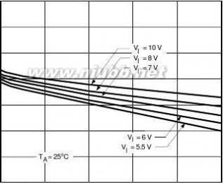
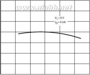
Output Volt. Temp. Coeff.Line RegulationLoad RegulationDropout VoltageQuiescent Current(GND terminal current)
αVO?VO(?VI)?VO(?IO)VImin - VO
IQ
IO = 0
5.5 V ≤ VI ≤ 10 V, Output open0 mA ≤ IO ≤ 500 mA?, VI = 6 VIO = 500 mA?
VI = 10 V, IO = 500 mA?VI = 10 V, Output open
IQ(off)
ENABLE Input Voltage
VEHVEL
ENABLE Input CurrentThermal Shutdown Temp.Thermal Resistance
IETJRθJARθJT
Typical values are given for circuit design information only.* This parameter is tested to a lot sample plan only.? Pulse test (<20 ms).
Min.4.904.85———————2.4———
Typ.5.00—±1001040—8786————165676.0
Max.5.105.15—3010030012012020—0.4±0.1———
UnitsVVμV/°CmVmVmVμAμAμAVVμA°C°C/W°C/W
VI = 10 V, Output open, VE = 0.4 VOutput ON, VI = 10 VOutput OFF, VI = 10 VVE = VI = 10 V
Mounted on 2.24" x 2.24" solder-coatedcopper-clad board in still air
——
8181 A8181中文资料
元器件交易网www.cecb2b.com
8181
LOW-DROPOUT,

5 V REGULATOR
扩展:stc12c5a60s2中文资料 / 8205a中文资料 / sim900a中文资料
TYPICAL CHARACTERISTICS
LOAD REGULATION
5.06
LINE REGULATION
5.06
5.04
OUTPUT VOLTAGE, VO in VOLTS
5.02
OUTPUT VOLTAGE, VO in VOLTS
5.04
5.02
5.00
5.00
4.98
4.98
4.96
4.96
4.94
4.94
4.92
100
200
300
400
500
OUTPUT CURRENT, IO in mA
Dwg. GP-039
4.92
5.0
6.0
7.0
8.0
9.0
INPUT VOLTAGE, VI in VOLTS
Dwg. GP-040
5.065.06
5.045.04
OUTPUT VOLTAGE, VO in VOLTS
OUTPUT VOLTAGE, VO in VOLTS
5.025.02
5.005.00
4.984.98
4.96
4.94

4.96
4.94
4.92
100
200
300
400
500
OUTPUT CURRENT, IO in mA
Dwg. GP-039-1
4.92
5.0
6.0
7.0
8.0
9.0
INPUT VOLTAGE, VI in VOLTS
Dwg. GP-040-1
CAUTION:
Maximum allowable duty cycle will be significantly less than 100% at high temperatures, at high input voltages, or at high output

currents. See Maximum Allowable Output Current table.
115 Northeast Cutoff, Box 15036
Worcester, Massachusetts 01615-0036 (508) 853-5000
8181 A8181中文资料
元器件交易网www.cecb2b.com
8181
LOW-DROPOUT,5 V REGULATOR

TYPICAL CHARACTERISTICS (cont’d)
LOAD REGULATION
5.06
5.06
LINE REGULATION
5.04
5.04

OUTPUT VOLTAGE, VO in VOLTS
5.02
OUTPUT VOLTAGE, VO in VOLTS
5.02
5.00
5.00
4.984.98
4.96
4.96
4.94
4.94
4.92
OUTPUT CURRENT, IO in mA
Dwg. GP-039-2
4.92
5.0
6.0
7.0
8.0
9.0
INPUT VOLTAGE, VI in VOLTS
Dwg. GP-040-2
DROPOUT VOLTAGE
0.5
OUTPUT VOLTAGE vs TEMP.
0.4
OUTPUT VOLTAGE, VO in VOLTS
DROPOUT VOLTAGE in VOLTS
0.3
5.01
5.004.99
0.2
4.98
0.1
-500+50+100
OUTPUT CURRENT, IO in mA
Dwg. GP-041
AMBIENT TEMPERATURE, TA in °C
Dwg. GP-036
CAUTION:
Maximum allowable duty cycle will be significantly less than 100% at high temperatures, at high input voltages, or at high output
currents. See Maximum Allowable Output Current table.
8181 A8181中文资料
元器件交易网www.cecb2b.com
8181
LOW-DROPOUT,

5 V REGULATOR
TYPICAL CHARACTERISTICS (cont’d)QUIESCENT (GROUND TERMINAL) CURRENT
81QUIESCENT (GROUND TERMINAL) CURRENT in μA
QUIESCENT (GROUND TERMINAL) CURRENT in μA
87

85
86
80
84
79
83
82
78
81
100
200
300
400
500
80
-500+50+100
AMBIENT TEMPERATURE, TA in °C
Dwg. GP-037
OUTPUT CURRENT, IO

in mA
Dwg. GP-038
TRANSIENT PERFORMANCE
90QUIESCENT (GROUND TERMINAL) CURRENT in μA
80
VI = 5.5 V to 10 V, TA = -20°C to +85°C, CO = 4.7 μF
70
60
VO
50
40
30
I
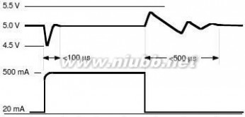
O
20Dwg. WP-018
Dwg. GP-042
INPUT VOLTAGE, VI in VOLTS
CAUTION:
Maximum allowable duty cycle will be significantly less than 100% at high temperatures, at high input voltages, or at high output
currents. See Maximum Allowable Output Current table.
115 Northeast Cutoff, Box 15036
Worcester, Massachusetts 01615-0036 (508) 853-5000
8181 A8181中文资料
元器件交易网www.cecb2b.com
8181LOW-DROPOUT,5 V REGULATOR
Dimensions in Inches(Based on 1 mm = 0.3937”)
扩展:stc12c5a60s2中文资料 / 8205a中文资料 / sim900a中文资料
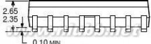

BSCDwg. MA-008-17A in
Dimensions in Millimeters
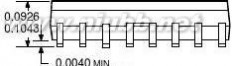

1.27BSCDwg. MA-008-17A mm
NOTES:1.Webbed lead frames. Leads 4, 5, 12, and 13 are internally one piece.
2.Lead spring tolerance is non-cumulative.
3.Exact body and lead configuration at vendor’s option within limits shown.
8181 A8181中文资料
元器件交易网www.cecb2b.com
8181LOW-DROPOUT,

5 V REGULATOR
Allegro MicroSystems, Inc. reserves the right to make, from time to time, such departures fromthe detail specifications as may be required to permit improvements in the design of its products.Components made under military approvals will be in accordance with the approval requirements.The information included herein is believed to be accurate and reliable. However, Allegro
MicroSystems, Inc. assumes no responsibility for its use; nor for any infringements of patents or otherrights of third parties which may result from its use.
115 Northeast Cutoff, Box 15036
Worcester, Massachusetts 01615-0036 (508) 853-5000
扩展:stc12c5a60s2中文资料 / 8205a中文资料 / sim900a中文资料
本文标题:中文资料-SSC-MGT7101中文资料61阅读| 精彩专题| 最新文章| 热门文章| 苏ICP备13036349号-1