一 : 2
2
二 : 2
王丽长得很漂亮,就连当时还是个小孩子,根本不懂什么叫做性诱惑的我看到了她,都会情不自禁地多望几眼。
她也是个好女孩。
出生在九镇附近不远的小乡村,贫穷的环境让她非常自强。一心想着考上北京上海的大学,改变自己和家人艰难的一生。
所以,她很努力。当她在初中会考上考出了全县第三名的成绩,却毅然决然放弃当时非常吃香,很多男生都梦寐以求的中专。转而选择离家近、可以更省钱的九镇高中,只为了一圆大学梦的消息传出之时。
轰动了全九镇。
一时之间,几乎每个学校,每个有着小孩的大人,都以她为榜样来教育自己的学生、儿女。
我当然也不例外。
很清楚的记得,有那么一段时间,外婆无数次带着期望的眼神给我说:
“老儿(九镇附近对于晚辈的昵称),今后长大了要学那个泉村的王家女伢儿,莫比一个女伢儿还差些啊。要考大学、读博士,帮大人争气。晓不晓得?”
这本是一个有着光明前途,美好未来的女孩,她的故事如果能够继续这样发展下去,在不久的将来,也许会成为一个鼓动人心的打拼成功史。
可惜,她所梦想中如同童话般美好的一切却最终没有实现。
因为,她爱上了一个人,一个完全改变了她所有生活的人。
那个人,就是姚义杰,坐在王丽旁边的同班同学。
姚义杰与王丽完全相反。
当时的他肯定不能说是一个坏人,但也绝对不是一个好学生。
举一个让我非常深刻的例子。记得很小的时候,某一次玩耍回家路过他家门前,听见他的爸爸在打他,边打边说:
“一百分的算数题,你给老子考了三分!!!!喊头猪来沾点墨水画勾勾,也不止得三分啊?老子要打死你个不争气的!”
当时年幼的我心底只有一个想法:那三哥就真是比猪还蠢啦。
不过没关系,成绩再烂,还有皮铁明这样的人垫底,加上还过得去的几门文科拉分,总的来说,不至于落到需要留级的最后三名。
他不算个好学生的关键地方在于——他的朋友。
那是一帮在大人老师们口中无恶不作,坏的头上长疮,脚底流脓的小流子(小混混),个个都迟早要被拉去枪毙。
虽然没有人见过或者听过姚义杰做了什么坏事,但是他一副尾大不掉的样子,叼着根烟,天天跟那些人满大街的晃,能学好吗?
变坏只是迟早的事而已。
其实,现在想起来,这些大人老师们真的猜中了。变坏确实只是迟早。
不过,他们没有猜想到的是,让姚义杰变坏的始作俑者并不是那些坏朋友,恰恰是这些好大人、大好人。
姚义杰班上的班主任人不坏,是个很认真,也很古板的老太太,对学生非常负责,她希望所有被她教出来的学生都能有出息,上大学。
所以,她做出了一个安排:
班上成绩最好的几个,每人负责一个,专门帮助、监督成绩最差的那几人,并且把每一对的位置调整成了同座。
成绩最好,最有威严,当班长的王丽,负责的那个人就是最不听话,胆子最大的姚义杰。
姚义杰的班主任得意地将这个安排取名为“一对一,两样红”。
具体是不是一对一我不太清楚。不过,没多长时间,这两个人在九镇是千真万确的红了,而且红得发紫。
刚开始,王丽和姚义杰两人度过了短暂的互不理睬之后,慢慢接触了起来。姚义杰的成绩也一如老师所料,开始提高,某段时间之内甚至是以飞速提升。
老师很开心,她看到了辛勤工作的回报。
只是,严肃古板的老太太又怎么会明白,朝夕相处之下,两位少男少女心中那种发自天性的懵懂春情。
无论在泡沫肥皂剧里面,还是现实生活中,都经常可以看到一件很奇怪,也很有趣的事情。
往往那些最听话,最懂事,又乖巧又漂亮的女学生,爱上的却是脸上挂着副轻佻、骄傲的笑容,成绩却是班上最差,最调皮捣蛋的那个男孩。
究竟是什么导致了这样的情况发生。
很简单,因为那些女孩太优秀。
[www.61k.com]优秀需要努力,而努力则是因为她们好强,好胜。她们坚信自己是与众不同,就算在最坏的男孩子心底也是一样。
她们会是男人最爱的那一个,也会是改变了男人的那一个。
所以,表露无疑的征服欲与藏在心底深处的被征服欲让她们往往都会不顾一切,去用行动来证明这一点。
王丽是个优秀的女孩,她也难以免俗。
不知道哪天开始,她的心底想用姚义杰来证明自己的绝对优秀了。
于是乎,原本完全不搭界的两个人相爱了,爱的死去活来。
只是,他们还太年轻,那个时候的他们并不明白这个世界上的女人从来就不能真正去改变一个男人。
正如,一个男人也永远不能改变女人。
热烈的爱情同时也让他们忘记了另一个更为致命的事情。
早恋!
发生在愚蒙未开的上个世界八十年代的早恋!
悲剧也就从这里开始诞生。
三 : Standby_v2-2
Power Supply Design Guideline 2004/11/12 Title: Standby Circuit Design REV.2.1
Power Supply Design Guideline
File Name: standby_v2.doc
Customer:
Version Page : V 2.1 : 8
- 1 -
Power Supply Design Guideline 2004/11/12 Title: Standby Circuit Design REV.2.1

- 2 -
Power Supply Design Guideline 2004/11/12 Title: Standby Circuit Design REV.2.1
[Input Side]
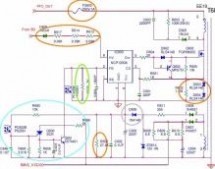


Fig1 typical prime side of NCP1200A standby circuit
Setting the Standby turn on voltage
Modifying R617,R614,R613, and R652 to decide Standby turned on voltage. UVLO
NCP1200 does not have UVLO function. NCP1201 support this function. Reducing Q603 peak voltage during AC ON/OFF rapidly and continuously
If Q603 Vds is over specification, it need to improve T600 transformer, add TVS diode, or increase R602.
Auto-Recover Circuit
The yellow region of Fig1 shows the Auto-Recover Protect Circuit. HV input Diode (D608)
The signal can connect form V380+ or BD. V380+ is suggested. Layout
C607 and C601 must be closed NCP1200A pin4(GND)
- 3 -

Power Supply Design Guideline 2004/11/12 Title: Standby Circuit Design REV.2.1

Skip Mode disable
NCP1200 Pin1 connects to GND, and IC will not operate in Skip Mode. If NCP1200 does not

disable Skip Mode, it might cause noise in light load.
Protect Current Sensing Resistor
In order to avoid Current Sensing resistor (R602) damage, paralleling pair diode in front and

back of R602.
Avoid duty cycle unstable in Short Current Mode

Adding R630 solves this issue.
Fuse choice.
Because the trace is thinner normally, it must use rapid breakdown fuse to avoid trace burn

away.
Why needs D609?
In order to keep Pin6 Vcc is about 12V (The maximum Vcc is 16V, designing about 12V

for IC)
Other
Install D609 to separate Vcc voltage form HV and Converter.
- 4 -
Power Supply Design Guideline 2004/11/12 Title: Standby Circuit Design REV.2.1

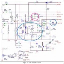
PS_Kill Function
The DC outputs, main(s) and Standby, will be disabled when the input is driven higher than 2.4V, or open circuited. The power supply Standby output will be enabled when this signal is pull low, below 0.8V. The main output(s) will be powered on or off based on –PS_ON. . In the low state the input will not source more than 0.5mA of current. Provisions for de-bouncing will be included in the PS_KILL circuitry to prevent the power supply from oscillating on/off at startup.
In Liteon design, Q632 is the MOS which reaches above function. Other design notices will be discussed below:
- 5 -
Power Supply Design Guideline 2004/11/12 Title: Standby Circuit Design REV.2.1
※ Adding a RC circuit to turn on/off PS_Kill SD
The circuit shows as RED circle. Adding the RC circuit to reduce the turned-on rate of
MOS(Q632), so the standby output voltage output overshoot and undershoot will be improve.
※ The PS_Kill MOS layout.
The PS_Kill MOS(Q632) must place in back of ORing Diode. To avoid the
overshoot & undershoot on +3.3VSB, we have immediately done the PS_KILL

function. The placement shows as blue circle.
The feedback circuit
The feedback circuit (show as Blue circle) could be soft start circuit. The rising time
of TL431’s reference voltage can be modified by the RC (R665, R645, and C640) circuit. Q604 base voltage could not too low, because it might cause dynamic character. The advantage of the RC and BJT circuit need smaller capacitor without big electrolytic capacitor.

TL431 application notice.
According TL431 specification, it needs a 1000pF capacitor to stabilize TL431.
- 6 -
Power Supply Design Guideline 2004/11/12 Title: Standby Circuit Design REV.2.1
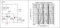
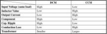
[Inductor Design]
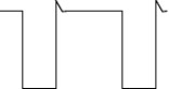
There are two kinds of operation modes in flyback converter: Discontinue Conduction Mode (DCM) and Continue Conduction Mode (CCM)
Vce
Ip
Ic
DCM
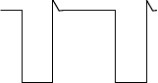
Ip1
CCM
Design tool

stanby v2.0.xls
- 7 -
Power Supply Design Guideline 2004/11/12 Title: Standby Circuit Design REV.2.1
◆ Dell request specification:
The maximum over/undershoot voltages will not exceed those defined below, and will not cause any over or under voltage detection circuits to activate. The load slew rate will not exceed 0.1A/uS. Frequency of the dynamic load will be 50Hz to 10kHz with a duty cycle of 10 to 90%. Frequency and duty cycle will be adjusted to produce the maximum amount of voltage transient on the output.
Output Level
+3.3V (SB) Maximum Load Step 1A Minimum Maximum Voltage Starting DC Load Starting DC Load Over/Undershoot 0.1A 3.9A +/-100mV
In order to fit the strict condition, it is important to select the components for output. Lower VF (forward voltage), Lower DCR, Lower Rds_on Components are the better choice.
The different makers of LM324 might cause bigger or smaller ripple noise. In Big Bend experience, STM or ON is a better choice.
- 8 -
Power Supply Design Guideline 2004/11/12 Title: Standby Circuit Design REV.2.1

1. Check Irms, Iave, Ipeak, and Vds,peak
2. Check Transformer Bmax.
3. TL431 is in stable region.
4. Protect function is latch or autorestart.
5. Check feedback photo-coupler is in linear region.
- 9 -
四 : 2
2
本文标题:2-261阅读| 精彩专题| 最新文章| 热门文章| 苏ICP备13036349号-1