一 : T5577卡片资料


Features
?Contactless Power Supply
?Contactless Read/Write Data Transmission
?Radio Frequency fRF from 100 kHz to 150 kHz
?Basic Mode or Extended Mode
?Compatible with T5557, ATA5567
?Replacement for e5551/T5551 in Most Common Operation Modes
?Configurable for ISO/IEC 11784/785 Compatibility
?Total 363 Bits EEPROM Memory: 11 Blocks (32 Bits + 1 Lock Bit)
?High Q-antenna Tolerance Due to Build in Options
?Adaptable to Different Applications: Access Control, Animal ID and Waste Management
?On-chip Trimmed An tenna Capacitor
?Pad Options
–ATA5577M1
?100μm × 100μm for Wire Bonding or Flip Chip
–ATA5577M2
?200μm × 400μm for Direct Coil Bonding
1.Description
The ATA5577 is a contactless read/write identification IC (IDIC?) for applications inthe 125-kHz or 134-kHz frequency band. A single coil connected to the chip serves asthe IC’s power supply and bi-directional communication interface. The antenna andchip together form a transponder or tag.
The on-chip 363-bit EEPROM (11 blocks with 33 bits each) can be read and writtenblock-wise from a base station (reader).
Data is transmitted from the IDIC (uplink) using load modulation. This is achieved bydamping the RF field with a resistive load between the two terminals Coil 1 and Coil 2.The IC receives and decodes serial base station commands (downlink), which areencoded as 100% amplitude modulated (OOK) pulse-interval-encoded bit streams.
A complete datasheet with further technical data is available on request. Please con-tact your local sales office.

2.Compatibility
The ATA5577 is designed to be compatible with the T5557/ATA5567. The structure of the con-figuration register is identical. The two modes, Basic mode and Extended mode, are alsoavailable. The ATA5577 is able to replace the e5551/T5551 in most common operation modes.In all applications, the correct functionality of the replacements must be evaluated and proved.For further details, refer to Atmel?’s web site for product-relevant application notes.
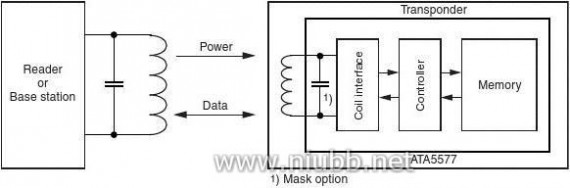
3.System Block Diagram
Figure 3-1.
RFID System Using ATA5577 Tag

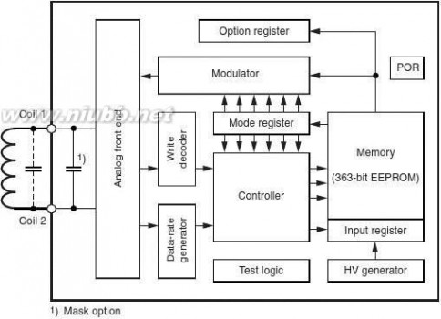
4.ATA5577 - Functional Blocks
Figure 4-1.
Block Diagram
2
ATA5577
4967DS–RFID–10/08

ATA5577
4.1Analog Front End (AFE)
The AFE includes all circuits that are directly connected to the coil terminals. It generates theIC's power supply and handles the bi-directional data communication with the reader. It consistsof the following blocks:
?Rectifier to generate a DC supply voltage from the AC coil voltage
?Clock extractor
?Switchable load between Coil 1 and Coil 2 for data transmission from the tag to the reader?Field-gap detector for data transmission from the base station to the tag
?ESD-protection circuitry
4.2Data-rate Generator
The data rate is binary programmable to operate at any even-numbered data rate between RF/2and RF/128 or to any of the fixed Basic mode data rates (RF/8, RF/16, RF/32, RF/40, RF/50,RF/64, RF/100 and RF/128).
4.3Write Decoder
The write decoder detects the write gaps and verifies the validity of the data stream according tothe Atmel e555x downlink protocol (pulse interval encoding).
4.4HV Generator
This on-chip charge pump circuit generates the high voltage required to program the EEPROM.
4.5DC Supply
Power is externally supplied to the IDIC via the two coil connections. The IC rectifies and regu-lates this RF source and uses it to generate its supply voltage.
4.6Power-On Reset (POR)
The power-on reset circuit blocks the voltage supply to the IDIC until an acceptable voltagethreshold has been reached.
4.7Clock Extraction
The clock extraction circuit uses the external RF signal as its internal clock source.
4.8Controller
The control logic module executes the following functions:
?Load mode register with configuration data from EEPROM block 0 after power-on and during reading
?Load option register with the settings for the analog front end stored in EEPROM page 1 block3 after power-on and during reading
?Control all EEPROM memory read/write access and data protection
?Handles the downlink command decoding detecting protocol violations and error conditions
3
4967DS–RFID–10/08

4.9Mode Register
The mode register maintains a readable shadow copy of the configuration data held in block0 ofthe EEPROM. It is continually refreshed during read mode and (re-)loaded after every PORevent or reset command. On delivery, the mode register is pre-programmed with default values(see full version of the datasheet).
4.10Modulator
The modulator encodes the serialized EEPROM data for transmission to a tag reader or basestation. Several types of modulation are available including Manchester, bi-phase, FSK, PSK,and NRZ.
4.11Memory
Figure 4-2.
0LPage 1
11LLLLPage 0
LLLLL
Memory Map
1.........................................................................................32
Analog front end option set-up
Traceability dataTraceability dataPage 0 configuration dataUser data or password
User dataUser dataUser dataUser dataUser dataUser dataConfiguration data
32 bits
Block 3Block 2Block 1Block 0Block 7Block 6Block 5Block 4Block 3Block 2Block 1Block 0
Not transmitted
The memory is a 363-bit EEPROM, which is arranged in 11 blocks of 33 bits each. Each blockincludes a single Lock bit, which is responsible for write-protecting the associated block. Pro-gramming takes place on a block basis, so a complete block (including lock bit) can beprogrammed with a single command. The memory is subdivided into two page areas. Page 0contains 8 blocks and page 1 contains 4 blocks. All 33 bits of a block, including the lock bit, areprogrammed simultaneously.
4
ATA5577
4967DS–RFID–10/08

ATA5577
Block 0 of page 0 contains the mode/configuration data, which is not transmitted during regularread operations. Addressing block 0 will always affect block 0 of page 0 re gardless of the pageselector. Block 7 of page 0 may be used as a write-protection password.
Block 3 of page 1 contains the option register, which is not transmitted during regular-readoperation.
Bit 0 of every block is the lock bit for that block. Once locked, the block (including the lock bititself) is not re-programmable via the RF field.
Blocks 1 and 2 of page 1 contain traceability data and are transmitted with the modulationparameters defined in the configuration register after the opcode “11” is issued by the reader.The traceability data blocks are programmed and locked by Atmel.
5.Absolute Maximum Ratings
Stresses beyond those listed under “Absolute Maximum Ratings” may cause permanent damage to the device. This is a stress rating only and functional operation of the device at these or any other conditions beyond those indicated in the operational sections of this specification is not implied. Exposure to absolute maximum rating conditions for extended periods may affect device reliability.Parameters
Maximum DC current into Coil1/Coil2
Maximum AC current into Coil1/Coil2, f = 125kHzPower dissipation (die) (free-air condition, time of application: 1s)
Electrostatic discharge maximum to
ANSI/ESD-STM5.1-2001 standard (HBM)Operating ambient temperature rangeStorage temperature range (data retention reduced)
SymbolIcoilIcoil pPtotVmaxTambTstg
Value20 (TBD)20 (TBD)100 (TBD)2000 (TBD)–40 to +85–40 to +150
UnitmAmAmWV°C°C
5
4967DS–RFID–10/08

6.Electrical Characteristics
Tamb = +25°C; fcoil = 125 kHz; unless otherwise specified No.12.12.22.33.13.23.345.15.25.35.46.16.26.36.46.57.17.27.37.47.57.689Notes:
Start-up timeParametersRF frequency range
Tamb = 25°C(1)
Supply current (without Read - full temperature current consumed by the range
external LC tank circuit)Programming - full
temperature range
POR threshold (50-mV hysteresis)
Coil voltage (AC supply)Read mode and write
command(2)
Program EEPROM(2)Vcoil pp = 6V
tstartupVpp clamp loVpp clamp medVpp clamp hiVpp clamp medVpp mod loVpp mod medVpp mod hiVpp mod medVmod lo/TambVclkdet loVclkdet medVclkdet hiVgapdet loVgapdet medVgapdet hiTprogncycle
TBDTBDTBDTBDTBDTBD5100000TBDTBDTBDTBDTBDTBDTBDTBD
Vcoil ppIDD
Test Conditions
SymbolfRF
Min.100
Typ.1251.5225
TBD68
2.5111317153577.5–12505508002505508505.7
TBDTBDTBDTBDTBDTBD6
3.6
Max.150TBDTBDTBDTBDVclampVclampTBDTBDTBDTBDTBDTBDTBDTBDTBD
UnitkHzμAμAμAVVVmsVVVVVVVVmV/°CmVmVmVmVmVmVmsCycles
TQQQQQQQQTTTQQTQQTQQTQTQType*
3-mA current into
Clamp voltage (depends Coil1/Coil2on settings in option register)
20-mA current into Coil1/Coil23-mA current into Coil1/Coil2 and
Modulation parameters modulation ON (depends on settings in option register)20 mA current into
Coil1/Coil2 and modulation ONThermal stability
Clock detection level
(depends on settings in Vcoil pp = 8Voption register)
Gap detection level
(depends on settings in Vcoil pp = 8 Voption register)
From last command gap to re-enter read mode (64 + 648 internal clocks)
Erase all/Write all(3)
Programming timeEndurance
*) Type means: T: directly or indirectly tested during production; Q: guaranteed based on initial product qualification data
1.IDD measurement set-up R = 100kΩ; VCLK = Vcoil = 3V: EEPROM programmed to 00 ... 000 (erase all); chip in modulation
defeat. IDD = (VOUTmax – VCLK)/R2.Current into Coil1/Coil2 is limited to 10 mA.
3.Since EEPROM performance is influenced by assembly processes, Atmel confirms the parameters for DOW (tested die on
uncut wafer) delivery.
6
ATA5577
4967DS–RFID–10/08

ATA5577
6.Electrical Characteristics (Continued)
Tamb = +25°C; fcoil = 125 kHz; unless otherwise specifiedNo.10.110.210.311.111.211.311.411.512.112.2Notes:
Micromodule capacitor parameters
Capacitance tolerance Tamb
Temperature coefficient
CrTBD
Resonance capacitor
Mask optionVcoil pp = 1V
Cr
Data retentionParameters
Test ConditionsTop = 55°C(3)Top = 150°C(3)Top = 250°C(3)
Symboltretentiontretentiontretention
Min.109624320242TBDTBDTBD320TBD
3302501307510330TBD
340258TBDTBDTBD340TBD
pFTBD
QTTBD
pF
Typ.20
Max.50
UnitYearshrshrs
Type*QTQT
*) Type means: T: directly or indirectly tested during production; Q: guaranteed based on initial product qualification data
1.IDD measurement set-up R = 100kΩ; VCLK = Vcoil = 3V: EEPROM programmed to 00 ... 000 (erase all); chip in modulation
defeat. IDD = (VOUTmax – VCLK)/R2.Current into Coil1/Coil2 is limited to 10 mA.
3.Since EEPROM performance is influenced by assembly processes, Atmel confirms the parameters for DOW (tested die on
uncut wa——文章窝——fer) delivery.
7.Revision History
Please note that the following page numbers referred to in this section refer to the specific revision mentioned, not to this document.Revision No.4967DS-RFID-10/084967CS-RFID-01/08
History
? Features on page 1 changed
? Features on page 1 changed
? Section 2 “Compatibility” on page 2 changed? Section 4.9 “Mode Register” on page 4 changed
? Put datasheet in a new template
? Section 4.2 “Data-rate Generator” on page 3 changed? Figure 4-2 “Memory Map” on page 5 changed
? Section 6 “Electrical Characteristics” numbers 2.1, 2.2 and 2.3 on page 6 changed
4967BS-RFID-09/07
7
4967DS–RFID–10/08

Headquarters
Atmel Corporation2325 Orchard ParkwaySan Jose, CA 95131USA
Tel: 1(408) 441-0311Fax: 1(408) 487-2600
International
Atmel AsiaRoom 1219
Chinachem Golden Plaza77 Mody Road TsimshatsuiEast KowloonHong Kong
Tel: (852) 2721-9778Fax: (852) 2722-1369
Atmel EuropeLe Krebs
8, Rue Jean-Pierre TimbaudBP 30978054
Saint-Quentin-en-YvelinesCedexFrance
Tel: (33) 1-30-60-70-00 Fax: (33) 1-30-60-71-11
Atmel Japan
9F, Tonetsu Shinkawa Bldg.1-24-8 Shinkawa
Chuo-ku, Tokyo 104-0033Japan
Tel: (81) 3-3523-3551Fax: (81) 3-3523-7581
Product Contact
Web Site
www.61k.com
Technical Supportrfid@atmel.com
Sales Contact
www.61k.comontacts
Literature Requestswww.61k.comliterature
Disclaimer: The information in this document is provided in connection with Atmel products. No license, express or implied, by estoppel or otherwise,to anyintellectualproperty right is granted by this document or in connection with the sale of Atmel products. EXCEPT AS SET FORTH IN ATMEL’S TERMS AND CONDI-TIONS OF SALE LOCATED ON ATMEL’S WEB SITE, ATMEL ASSUMES NO LIABILITY WHATSOEVER AND DISCLAIMS ANY EXPRESS, IMPLIED OR STATUTORYWARRANTY RELATING TO ITS PRODUCTS INCLUDING, BUT NOT LIMITED TO, THE IMPLIED WARRANTY OF MERCHANTABILITY, FITNESS FOR A PARTICULARPURPOSE, OR NON-INFRINGEMENT. IN NO EVENT SHALL ATMEL BE LIABLE FOR ANY DIRECT, INDIRECT, CONSEQUENTIAL, PUNITIVE, SPECIAL OR INCIDEN-TAL DAMAGES (INCLUDING, WITHOUT LIMITATION, DAMAGES FOR LOSS OF PROFITS, BUSINESS INTERRUPTION, OR LOSS OF INFORMATION) ARISING OUT OFTHE USE OR INABILITY TO USE THIS DOCUMENT, EVEN IF ATMEL HAS BEEN ADVISED OF THE POSSIBILITY OF SUCH DAMAGES. Atmel makes n orepresentationsor warranties with respect to the accuracy or completeness of the contents of this document and reserves the right to make changes to specificationsand product descriptions at any time without notice. Atmel does not make any commitment to update the information contained herein. Unless specifically providedotherwise, Atmel products are not suitable for, and shall not be used in, automotive applications. Atmel’s products are not intended, authorized, or warranted for useas components in applications intended to support or sustainlife.
? 2008 Atmel Corporation. All rights reserved. Atmel?, logo and combinations thereof, IDIC? and others are registered trademarks or trade-marks of Atmel Corporation or its subsidiaries. Other terms and product names may be trademarks of others.
4967DS–RFID–10/08
二 : 关于74HC244芯片的中文资料24
求关于74HC244芯片的中文资料
54/74LS244
三态八缓冲器/线驱动器/线接收器(3S,两组控制)
简要说明:
244为三态输出的八组缓冲器和总线驱动器,其主要电器特性的典型值如下(不同厂家具体值有差别):
型号 tPLH tphl PD
54LS241/74LS241 12ns 12ns 110mW
引出端符号:
1A1~1A4,2A1~2A4 输入端
/1G, /2G 三态允许端(低电平有效)
1Y1~1Y4,2Y1~2Y4 输出端
逻辑图:
双列直插封装
极限值:
电源电压 …………………………………………. 7V
输入电压 …………………………………………. 5.5V
输出高阻态时高电平电压 …………………………. 5.5V
工作环境温度
54XXX …………………………………. -55~125℃
74XXX …………………………………. 0~70℃
存储温度 …………………………………………. -65~150℃
功能表:
推荐工作条件:
54LS244/74LS244 单位
最小 额定 最大
电源电压Vcc 54 4.5 5 5.5 V
74 4.75 5 5.25
输入高电平电ViH 2 V
输入低电平电ViL 54 0.7 V
74 0.8
输出高电平电流IOH 54 -12 mA
74 -15
输出低电平电流IOL 54 12 mA
74 24
动态特性(TA=25℃)
参 数 测 试 条 件 LS244 单位
最 大
tPLH输出由低到高传输延迟时间 Vcc =5V
CL=45pF
RL=667 Ω
18 ns
tPHL输出由高到低传输延迟时间 18 ns
tPZH输出由高阻态到高允许时间 23 ns
tPZL输出由高阻态到低允许时间 30 ns
tPHZ输出由高到高阻态禁止时间 Vcc=5V CL=5pF
RL=90 Ω 18 ns
tPLZ输出由低到高阻态禁止时间 25 ns
静态特性(TA为工作环境温度范围)
参 数 测 试 条 件【1】 LS244 单位
最小 最大
VIK输入嵌位电压 Vcc=最小,Iik=-18mA -1.5 V
△VT滞后电压 Vcc=最小 0.2 V
VOH输出高电平电压 Vcc=最小,VIL=最大,VIH=2V,
IOH=-3mA 2.4 V
VOL输出低电平电压 Vcc=最小,VIL=最大, IOL=最大 54 0.4 V
74 0.5
II最大输入电压时输出电流 Vcc=最大,VI=7V 0.1 mA
IIH输入高电平电流 Vcc=最大,VIH=2.7V 20 uA
IIL输入低电平电流 1A,2A Vcc=最大,VIL=0.4V -0.2 mA
IOS输出短路电流 Vcc=最大 -40 -225 mA
IOZH输出高阻态时高电平电流 Vcc=最大,VIH=2V
VIL=最大,VO=2.7V 20 uA
IOZL输出高阻态时低电平电流 Vcc=最大,VIH=2V,VIL=最大
,VO=0.4V -20 uA
Icc电源电流 Vcc=最大 1Y,2Y均为高电平 27 mA
1Y,2Y均为低电平 46
1Y,2Y均为高阻态 54
[1]: 测试条件中的“最小”和“最大”用推荐工作条件中的相应值。
三 : 关于运动的资料
流水不腐,户枢不蠹,动也。(吕不韦)以自然之道,养自然之身.(欧阳修)生命在于运动。(伏尔泰)运动是一切生命的源泉。(达.芬奇)只有运动才可以除去各种各样的疑虑。(歌德)生命就是运动,人的生命就是运动。(列夫.托尔斯泰)育运动名言
如果你想强壮,跑步吧! 如果你想健美,跑步吧!如果你想聪明,跑步吧!古希腊格言
★ 生命在于运动.(法国启蒙思想家——伏尔泰)★ 生命需要运动.(希腊哲学家——亚里斯多德)★ 科学的基础是健康的身体.(波兰科学家——居里夫人)★ 运动的作用可以代替药物,但所有的药物都不能替代运动。(法国医学家——蒂素)★ 身体虚弱,它将永远不全培养有活力的灵魂和智慧。(德国诗人——卢梭)★ 世上没有比结实的肌肉和新鲜的皮肤更美丽的衣裳。(俄国诗人——马雅可夫斯基)● 运动太多和太少,同样的损伤体力;饮食过多与过少,同样的损伤健康;唯有适度可以 产生、增进、保持体力和健康。——亚里士多德
●日复一日地坚持练下去吧,只有活动适量才能保持训练的热情和提高运动的技能。塞涅卡
● 运动是一切生命的源泉。——达·芬奇
1个埋头脑力劳动的人,如果不经常活动四肢,那是一件极其痛苦的事情。—列夫·托尔斯泰
● 我生平喜欢步行,运动给我带来了无穷的乐趣。——爱因斯坦
● 静止便是死亡,只有运动才能敲开永生的大门。——泰戈尔
●生活多美好啊,体育锻炼乐趣无穷。——普希金
列宁:在我们劳动人民的国家内,需要千百万身体健壮、意志坚强、勇敢无畏、朝气蓬勃、坚韧不拔的人。
毛泽东发展体育运动,增强人民体质。
朱德努力发展体育事业,把我们的国民锻炼成为身体健康精神愉快的人。
皮埃尔·顾拜旦
1个民族,老当益壮的人多,那个民族一定强;1个民族,未老先衰的人多,那个民族一定弱。
新加坡内阁资政李光耀每天长跑20分钟
新加坡前总理、现内阁资政李光耀已年过古稀,但仍然头脑清楚、精神饱满、腿脚利落。
不论在家还是出国,每天雷打不动坚持长跑20分钟。李光耀说:“我每天都做运动,如果不做(www.61k.com),便感到懒散,我发现健身操使我感觉更好,能开胃,也睡得更好。”李光耀经常从事的运动项目除了跑步外,还有游泳和骑自行车。如果是应邀去没有运动设施的国家开会,他的随身行李一定要带着可折叠的健身脚踏车,清晨或晚饭前进行运动。李光耀认为,有了运动,还要有足够的休息才能健康,每天睡眠8个小时最理想,但通常他只睡六7个小时,因为睡眠质量好,从不失眠。
李光耀曾是个胖子,喜欢吃炸鸡翅,喝啤酒和葡萄酒。他现在这副身板,都是他努力进行体育锻炼的结果。他特别倡导体育运动,他认为居住在城市里的人,必须注意锻炼身体,这方面他也率先做到了。
各国小朋友,北京来相会。 飘起奥运旗,戴起奥运徽。
绿色奥运好,口号提的美 更快又更高,更强又更美。
大家齐努力,金牌乖乖回。
迎接奥运忙
(学生) 钱雨莹
古老北京城呀, 一天1个样。 高楼拔地起呀, 道路宽又长。
河水清又清呀, 花草吐芬芳。 人人笑开怀呀, 迎接奥运忙。
四 : T5577卡片资料


Features
?Contactless Power Supply
?Contactless Read/Write Data Transmission
?Radio Frequency fRF from 100 kHz to 150 kHz
?Basic Mode or Extended Mode
?Compatible with T5557, ATA5567
?Replacement for e5551/T5551 in Most Common Operation Modes
?Configurable for ISO/IEC 11784/785 Compatibility
?Total 363 Bits EEPROM Memory: 11 Blocks (32 Bits + 1 Lock Bit)
?High Q-antenna Tolerance Due to Build in Options
?Adaptable to Different Applications: Access Control, Animal ID and Waste Management
?On-chip Trimmed Antenna Capacitor
?Pad Options
–ATA5577M1
?100μm × 100μm for Wire Bonding or Flip Chip
–ATA5577M2
?200μm × 400μm for Direct Coil Bonding
1.Description
The ATA5577 is a contactless read/write identification IC (IDIC?) for applications inthe 125-kHz or 134-kHz frequency band. A single coil connected to the chip serves asthe IC’s power supply and bi-directional communication interface. The antenna andchip together form a transponder or tag.
The on-chip 363-bit EEPROM (11 blocks with 33 bits each) can be read and writtenblock-wise from a base station (reader).
Data is transmitted from the IDIC (uplink) using load modulation. This is achieved bydamping the RF field with a resistive load between the two terminals Coil 1 and Coil 2.The IC receives and decodes serial base station commands (downlink), which areencoded as 100% amplitude modulated (OOK) pulse-interval-encoded bit streams.
A complete datasheet with further technical data is available on request. Please con-tact your local sales office.
5577 T5577卡片资料

2.Compatibility
The ATA5577 is designed to be compatible with the T5557/ATA5567. The structure of the con-figuration register is identical. The two modes, Basic mode and Extended mode, are alsoavailable. The ATA5577 is able to replace the e5551/T5551 in most common operation modes.In all applications, the correct functionality of the replacements must be evaluated and proved.For further details, refer to Atmel?’s web site for product-relevant application notes.
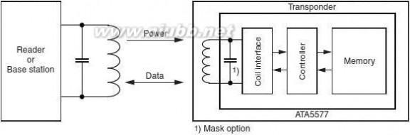
3.System Block Diagram
Figure 3-1.
RFID System Using ATA5577 Tag
4.ATA5577 - Functional Blocks
Figure 4-1.
Block Diagram
2
ATA5577
4967DS–RFID–10/08
5577 T5577卡片资料

ATA5577
4.1Analog Front End (AFE)
The AFE includes all circuits that are directly connected to the coil terminals. It generates theIC's power supply and handles the bi-directional data communication with the reader. It consistsof the following blocks:
?Rectifier to generate a DC supply voltage from the AC coil voltage
?Clock extractor
?Switchable load between Coil 1 and Coil 2 for data transmission from the tag to the reader?Field-gap detector for data transmission from the base station to the tag
?ESD-protection circuitry
4.2Data-rate Generator
The data rate is binary programmable to operate at any even-numbered data rate between RF/2and RF/128 or to any of the fixed Basic mode data rates (RF/8, RF/16, RF/32, RF/40, RF/50,RF/64, RF/100 and RF/128).
4.3Write Decoder
The write decoder detects the write gaps and verifies the validity of the data stream according tothe Atmel e555x downlink protocol (pulse interval encoding).
4.4HV Generator
This on-chip charge pump circuit generates the high voltage required to program the EEPROM.
4.5DC Supply
Power is externally supplied to the IDIC via the two coil connections. The IC rectifies and regu-lates this RF source and uses it to generate its supply voltage.
4.6Power-On Reset (POR)
The power-on reset circuit blocks the voltage supply to the IDIC until an acceptable voltagethreshold has been reached.
4.7Clock Extraction
The clock extraction circuit uses the external RF signal as its internal clock source.
4.8Controller
The control logic module executes the following functions:
?Load mode register with configuration data from EEPROM block 0 after power-on and during reading
?Load option register with the settings for the analog front end stored in EEPROM page 1 block3 after power-on and during reading
?Control all EEPROM memory read/write access and data protection
?Handles the downlink command decoding detecting protocol violations and error conditions
3
4967DS–RFID–10/08
5577 T5577卡片资料

4.9Mode Register
The mode register maintains a readable shadow copy of the configuration data held in block0 ofthe EEPROM. It is continually refreshed during read mode and (re-)loaded after every PORevent or reset command. On delivery, the mode register is pre-programmed with default values(see full version of the datasheet).
4.10Modulator
The modulator encodes the serialized EEPROM data for transmission to a tag reader or basestation. Several types of modulation are available including Manchester, bi-phase, FSK, PSK,and NRZ.
4.11Memory
Figure 4-2.
0LPage 1
11LLLLPage 0
LLLLL
Memory Map
1.........................................................................................32
Analog front end option set-up
Traceability dataTraceability dataPage 0 configuration dataUser data or password
User dataUser dataUser dataUser dataUser dataUser dataConfiguration data
32 bits
Block 3Block 2Block 1Block 0Block 7Block 6Block 5Block 4Block 3Block 2Block 1Block 0
Not transmitted
The memory is a 363-bit EEPROM, which is arranged in 11 blocks of 33 bits each. Each blockincludes a single Lock bit, which is responsible for write-protecting the associated block. Pro-gramming takes place on a block basis, so a complete block (including lock bit) can beprogrammed with a single command. The memory is subdivided into two page areas. Page 0contains 8 blocks and page 1 contains 4 blocks. All 33 bits of a block, including the lock bit, areprogrammed simultaneously.
4
ATA5577
4967DS–RFID–10/08
5577 T5577卡片资料

ATA5577
Block 0 of page 0 contains the mode/configuration data, which is not transmitted during regularread operations. Addressing block 0 will always affect block 0 of page 0 regardless of the pageselector. Block 7 of page 0 may be used as a write-protection password.
Block 3 of page 1 contains the option register, which is not transmitted during regular-readoperation.
Bit 0 of every block is the lock bit for that block. Once locked, the block (including the lock bititself) is not re-programmable via the RF field.
Blocks 1 and 2 of page 1 contain traceability data and are transmitted with the modulationparameters defined in the configuration register after the opcode “11” is issued by the reader.The traceability data blocks are programmed and locked by Atmel.
5.Absolute Maximum Ratings
Stresses beyond those listed under “Absolute Maximum Ratings” may cause permanent damage to the device. This is a stress rating only and functional operation of the device at these or any other conditions beyond those indicated in the operational sections of this specification is not implied. Exposure to absolute maximum rating conditions for extended periods may affect device reliability.Parameters
Maximum DC current into Coil1/Coil2
Maximum AC current into Coil1/Coil2, f = 125kHzPower dissipation (die) (free-air condition, time of application: 1s)
Electrostatic discharge maximum to
ANSI/ESD-STM5.1-2001 standard (HBM)Operating ambient temperature rangeStorage temperature range (data retention reduced)
SymbolIcoilIcoil pPtotVmaxTambTstg
Value20 (TBD)20 (TBD)100 (TBD)2000 (TBD)–40 to +85–40 to +150
UnitmAmAmWV°C°C
5
4967DS–RFID–10/08
5577 T5577卡片资料

6.Electrical Characteristics
Tamb = +25°C; fcoil = 125 kHz; unless otherwise specifiedNo.12.12.22.33.13.23.345.15.25.35.46.16.26.36.46.57.17.27.37.47.57.689Notes:
Start-up timeParametersRF frequency range
Tamb = 25°C(1)
Supply current (without Read - full temperature current consumed by the range
external LC tank circuit)Programming - full
temperature range
POR threshold (50-mV hysteresis)
Coil voltage (AC supply)Read mode and write
command(2)
Program EEPROM(2)Vcoil pp = 6V
tstartupVpp clamp loVpp clamp medVpp clamp hiVpp clamp medVpp mod loVpp mod medVpp mod hiVpp mod medVmod lo/TambVclkdet loVclkdet medVclkdet hiVgapdet loVgapdet medVgapdet hiTprogncycle
TBDTBDTBDTBDTBDTBD5100000TBDTBDTBDTBDTBDTBDTBDTBD
Vcoil ppIDD
Test Conditions
SymbolfRF
Min.100
Typ.1251.5225
TBD68
2.5111317153577.5–12505508002505508505.7
TBDTBDTBDTBDTBDTBD6
3.6
Max.150TBDTBDTBDTBDVclampVclampTBDTBDTBDTBDTBDTBDTBDTBDTBD
UnitkHzμAμAμAVVVmsVVVVVVVVmV/°CmVmVmVmVmVmVmsCycles
TQQQQQQQQTTTQQTQQTQQTQTQType*
3-mA current into
Clamp voltage (depends Coil1/Coil2on settings in option register)
20-mA current into Coil1/Coil23-mA current into Coil1/Coil2 and
Modulation parameters modulation ON (depends on settings in option register)20 mA current into
Coil1/Coil2 and modulation ONThermal stability
Clock detection level
(depends on settings in Vcoil pp = 8Voption register)
Gap detection level
(depends on settings in Vcoil pp = 8 Voption register)
From last command gap to re-enter read mode (64 + 648 internal clocks)
Erase all/Write all(3)
Programming timeEndurance
*) Type means: T: directly or indirectly tested during production; Q: guaranteed based on initial product qualification data
1.IDD measurement set-up R = 100kΩ; VCLK = Vcoil = 3V: EEPROM programmed to 00 ... 000 (erase all); chip in modulation
defeat. IDD = (VOUTmax – VCLK)/R2.Current into Coil1/Coil2 is limited to 10 mA.
3.Since EEPROM performance is influenced by assembly processes, Atmel confirms the parameters for DOW (tested die on
uncut wafer) delivery.
6
ATA5577
4967DS–RFID–10/08
5577 T5577卡片资料

ATA5577
6.Electrical Characteristics (Continued)
Tamb = +25°C; fcoil = 125 kHz; unless otherwise specifiedNo.10.110.210.311.111.211.311.411.512.112.2Notes:
Micromodule capacitor parameters
Capacitance tolerance Tamb
Temperature coefficient
CrTBD
Resonance capacitor
Mask optionVcoil pp = 1V
Cr
Data retentionParameters
Test ConditionsTop = 55°C(3)Top = 150°C(3)Top = 250°C(3)
Symboltretentiontretentiontretention
Min.109624320242TBDTBDTBD320TBD
3302501307510330TBD
340258TBDTBDTBD340TBD
pFTBD
QTTBD
pF
Typ.20
Max.50
UnitYearshrshrs
Type*QTQT
*) Type means: T: directly or indirectly tested during production; Q: guaranteed based on initial product qualification data
1.IDD measurement set-up R = 100kΩ; VCLK = Vcoil = 3V: EEPROM programmed to 00 ... 000 (erase all); chip in modulation
defeat. IDD = (VOUTmax – VCLK)/R2.Current into Coil1/Coil2 is limited to 10 mA.
3.Since EEPROM performance is influenced by assembly processes, Atmel confirms the parameters for DOW (tested die on
uncut wafer) delivery.
7.Revision History
Please note that the following page numbers referred to in this section refer to the specific revision mentioned, not to this document.Revision No.4967DS-RFID-10/084967CS-RFID-01/08
History
? Features on page 1 changed
? Features on page 1 changed
? Section 2 “Compatibility” on page 2 changed? Section 4.9 “Mode Register” on page 4 changed
? Put datasheet in a new template
? Section 4.2 “Data-rate Generator” on page 3 changed? Figure 4-2 “Memory Map” on page 5 changed
? Section 6 “Electrical Characteristics” numbers 2.1, 2.2 and 2.3 on page 6 changed
4967BS-RFID-09/07
7
4967DS–RFID–10/08
5577 T5577卡片资料

Headquarters
Atmel Corporation2325 Orchard ParkwaySan Jose, CA 95131USA
Tel: 1(408) 441-0311Fax: 1(408) 487-2600
International
Atmel AsiaRoom 1219
Chinachem Golden Plaza77 Mody Road TsimshatsuiEast KowloonHong Kong
Tel: (852) 2721-9778Fax: (852) 2722-1369
Atmel EuropeLe Krebs
8, Rue Jean-Pierre TimbaudBP 30978054
Saint-Quentin-en-YvelinesCedexFrance
Tel: (33) 1-30-60-70-00 Fax: (33) 1-30-60-71-11
Atmel Japan
9F, Tonetsu Shinkawa Bldg.1-24-8 Shinkawa
Chuo-ku, Tokyo 104-0033Japan
Tel: (81) 3-3523-3551Fax: (81) 3-3523-7581
Product Contact
Web Site
www.atmel.com
Technical Supportrfid@atmel.com
Sales Contact
www.atmel.com/contacts
Literature Requestswww.atmel.com/literature
Disclaimer: The information in this document is provided in connection with Atmel products. No license, express or implied, by estoppel or otherwise,to anyintellectualproperty right is granted by this document or in connection with the sale of Atmel products. EXCEPT AS SET FORTH IN ATMEL’S TERMS AND CONDI-TIONS OF SALE LOCATED ON ATMEL’S WEB SITE, ATMEL ASSUMES NO LIABILITY WHATSOEVER AND DISCLAIMS ANY EXPRESS, IMPLIED OR STATUTORYWARRANTY RELATING TO ITS PRODUCTS INCLUDING, BUT NOT LIMITED TO, THE IMPLIED WARRANTY OF MERCHANTABILITY, FITNESS FOR A PARTICULARPURPOSE, OR NON-INFRINGEMENT. IN NO EVENT SHALL ATMEL BE LIABLE FOR ANY DIRECT, INDIRECT, CONSEQUENTIAL, PUNITIVE, SPECIAL OR INCIDEN-TAL DAMAGES (INCLUDING, WITHOUT LIMITATION, DAMAGES FOR LOSS OF PROFITS, BUSINESS INTERRUPTION, OR LOSS OF INFORMATION) ARISING OUT OFTHE USE OR INABILITY TO USE THIS DOCUMENT, EVEN IF ATMEL HAS BEEN ADVISED OF THE POSSIBILITY OF SUCH DAMAGES. Atmel makes norepresentationsor warranties with respect to the accuracy or completeness of the contents of this document and reserves the right to make changes to specificationsand product descriptions at any time without notice. Atmel does not make any commitment to update the information contained herein. Unless specifically providedotherwise, Atmel products are not suitable for, and shall not be used in, automotive applications. Atmel’s products are not intended, authorized, or warranted for useas components in applications intended to support or sustainlife.
? 2008 Atmel Corporation. All rights reserved. Atmel?, logo and combinations thereof, IDIC? and others are registered trademarks or trade-marks of Atmel Corporation or its subsidiaries. Other terms and product names may be trademarks of others.
4967DS–RFID–10/08
五 : 关于运动的话题(黑板报小资料)_紫客幽兰
名人谈运动
“运动是自己命运的创造者”这是诺贝尔奖得主谢灵顿的至理名言;“运动是目的,理想是标准”这是法国文学家雨果的一生追求;“只有运动,生活才会不断进步”这是英国戏曲家莎士比亚的真诚信仰;“一生的运动是永远的青春”这是一代伟人毛主席的成功法宝。的确,生命在于不断运动,只有运动才能把握短暂的青春,只有运动才能让生活变得更加富有情趣,只有运动才能提高人们的审美意识;只有运动才能让人间处处充满团结、友爱。运动是永远不会过时的话题。
积极运动,珍爱生命
会有越来越多的人更加珍爱生命、更加关注健康。因为,放眼五洲四海,整个世界正朝着和平与进步的方向发展。人类的生存环境好了,生命也才变得更加宝贵。再俯首看看自己,虽然拥有健康并不等于就拥有了一切,但失去了健康,必将失去一切。
自己以及他人的健康,我们应该严格的遵守学校对于防控流感疫情而实施的措施,自觉量体温,一发现异常,立即报告班主任。从细微处做起,爱自己就是爱他人。
我运动,我快乐
运动是力量的角逐,是智慧的较量,更是美的展示。太阳无语,却放射着光辉;高山无语,却体现着巍峨;蓝天无语,却表露着深远。古希腊有这样一段格言:如果你想聪明,跑步吧!如果你想健康,跑步吧!在这里我要和我们的孩子一起大声说:如果你想拥有健康的心灵,如果你想拥有强壮的体魄,如果你想拥有成功的人生,请来参加运动吧!因为我运动?我健康?我快乐!
运动的好处
我们运动,可以接受阳光的照射,弥补阳光照射的不足。阳光中的紫外线不但能杀死人体皮肤、衣服上的病毒和病菌,对人体有消毒作用。还能促进身体对钙、磷的吸收作用,有助于骨骼的生长发育。尤其对正在长身体的青少年来说,多参加户外锻炼更为重要,还可以加快血液循坏,增加了大脑氧气的供应量,这对消除大脑长期工作带来的疲劳,增强记忆力,提高学习效率,都有积极的作用。
双手摩擦搓手的好处
经常将双手在一起摩擦搓手,主要有以下三个方面的好处: 一是常在户外工作的人,这么做可以预防冻疮的发生。 二是常搓双手,能使手指更加灵活自如,同时对大脑也有一定的保健作用。 三是生活和工作于室内的人,经常这样搓手,能促进血液循环和新陈代谢,预防感冒。对流活动。还有汽车排放出的尾气,其中含有氮氧化物、碳氢化物、铅等污染物质,各种有害物质聚于地面,不能向空气上层扩散,故沉积停留在人们的呼吸道,使人吸入更多的烟尘和有毒气体。
健康需要运动
健康需要运动,运动促进健康。只有时时刻刻来锻炼自己的,纠正自己的心态,运动自己的体魄,才能拥有一颗健康的心,一颗青春的心。快乐有苦有甜,有酸有涩。人生时见阴云,时见阳光。在运动中,我们可以体会到五味生活,七彩人生。运动传递健康,健康成就快乐。运动——一个永远不会落下的大浪,一颗最闪亮的星星,一束最灿烂的花朵,它永远诠释着生命的最高境界,永远披露着团结的真正含义,永远揭示着努力的最后回报。运动让生命更加富有生机,让生命为之颤动!
本文标题:关于运动的资料卡片-T5577卡片资料 61阅读| 精彩专题| 最新文章| 热门文章| 苏ICP备13036349号-1