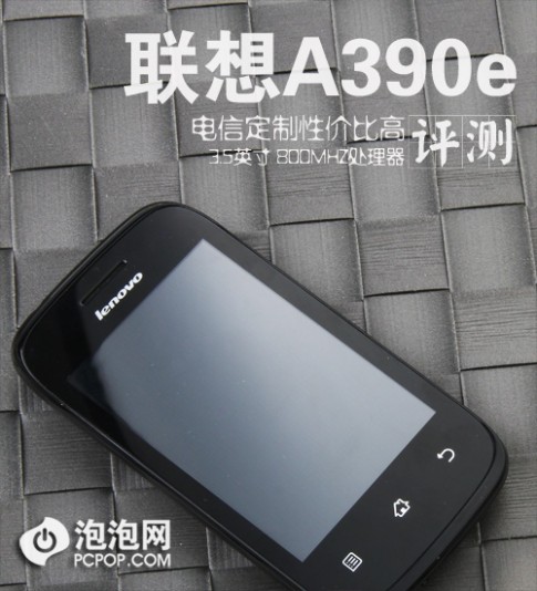
一 : 3.5寸触摸屏 电信定制联想A390e评测
文/董晓龙
新的一年马上就要到了,而对于很多大学生来说马上又要放寒假了,对于很多年轻的白领来说领了年终奖以后也要放年假了。俗话说新年新气象,什么都讲究一个“新”字,相信一定有很多朋友打算换一部新手机。无论是大学生,还是入职不久的白领,都是年轻人,年轻人就应该拥有年轻人的手机。今天小编带来的评测就是这样一款主打年轻人市场的产品:联想A390e。
点击图片查看联想A390e详细资料
这是一款中国电信定制的新机,经典的外观设计,优雅的细节处理,简约的PDA造型,加上“钢琴黑”的第一配色,更加提升了产品层次感,更显大气。11.5mm的纤薄机身,加上优雅花纹的电池后盖设计,整机更加突显产品独有的品位。
如果你是一个追求时尚、新潮的年轻人,如果你也关注联想A390e这款手机,那就随着小编一起进入今天的评测吧。
机身外观 设计经典细节之处优雅
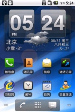
首先还是从外观方面看,联想A390e这款手机采用的是黑色设计。3.5英寸的电容触控屏,分辨率为480×320像素,支持多点触控。屏幕上方为“lenovo”标志,手机听筒以及光线感应器,没有前置摄像头。不过右上角有一个时尚动感的呼吸灯。下方则是三个触摸按键,分别可以实现Memu、Home以及返回功能。

图为:联想A390e手机


图为:联想A390e手机
机身背面采用钢琴烤漆的材质,带有横向的弧形调味,看起来非常舒服,尽显优雅。不过缺点就是容易沾染指纹。由于该机是由中国电信定制,所以在机身背部印有天翼的logo。

图为:联想A390e手机


图为:联想A390e手机
背面顶部是一颗320万像素的摄像头,没有配备LED闪光灯,略显遗憾。至于样片质量如何,在文章的后面会有展示。
接口电池 3.5mm耳机MicroUSB数据线
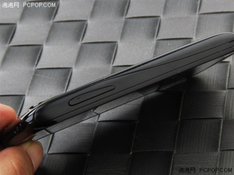
联想A390e的侧面设计非常简洁。简洁到机身左侧什么功能键有没有,不过可以看到机身后盖同样采用弧形设计,富有动感。

图为:联想A390e手机
机身右侧也只有音量调节键,并没有配备拍照快捷键。其实现在很多智能手机都没有拍照快捷键了,更多采用的是屏幕触控的方式。
图为:联想A390e手机
机身顶部的功能键大家也都看到了,右侧是电源/解锁键,左侧是3.5mm的耳机接口。

图为:联想A390e手机
机身底部只有Micro USB数据线接口,可以实现数据的传输以及给电池充电的功能。

图为:联想A390e手机
拆开后盖,可以看到存储卡与手机卡的位置都比较明显。从图片中也可以看到,电池的容量为1300mAh。经过实际使用,这款手机还是比较省电的。

图为:联想A390e手机

图为:联想A390e手机
值得一提的是,该机在出售的时候会随即附送2GB的存储卡,基本可以满足日常的生活需求。如果选择存放较大的视频或者音频文件,也可以自行购买一张更大的存储卡。
系统界面 安卓原生系统运行流畅
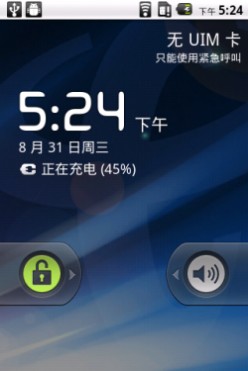
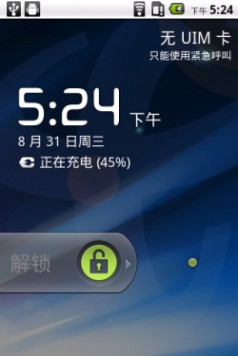
外观评测到此就说完了,一起看看系统和应用吧。联想A390e采用的是大家所熟知和喜爱的Android 2.2.2版本。界面也是安卓原生界面,所以解锁方式也是最经典的样式。
图为:联想A390e手机菜单
图为:联想A390e手机菜单
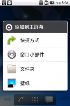
默认主屏为五屏,用户可以根据自己的需要在上面添加软件的快捷方式以及各式各样的小插件。

图为:联想A390e手机菜单
例如时钟、天气预报、人人网、微博等等。当然,方法相信大家都很熟悉,手指长按屏幕空白处就可以了。

图为:联想A390e手机菜单
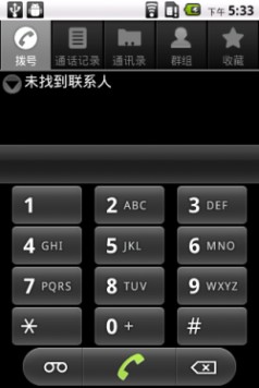
拨号界面和短信界面均为安卓原生,没有什么变化。编辑短信内容的时候,输入法具有联想功能,输入常见词汇的时候还是很方便的。

图为:联想A390e手机菜单
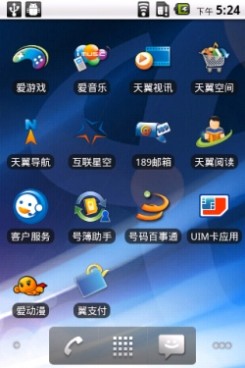
进入手机主菜单,可以看到该机内置了很多应用程序,例如腾讯QQ、新浪微博、腾讯微博、UC浏览器等等,由于这些程序都非常常见,所以就不做过多介绍。
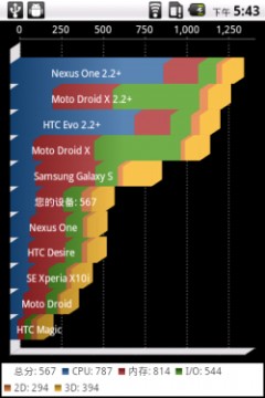
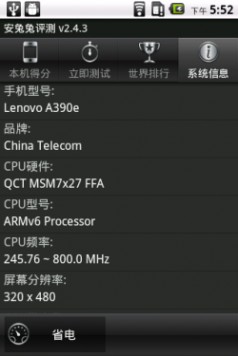
性能测试 跑分虽一般操控却流畅
下面进行的是跑分测试。首先是用性能测试高级版跑一下,由于该机配置一般,所以大家还需理性看待。
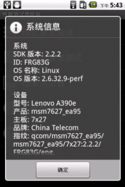
图为:联想A390e手机菜单
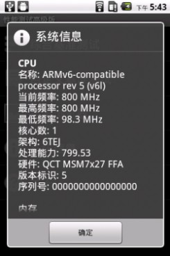
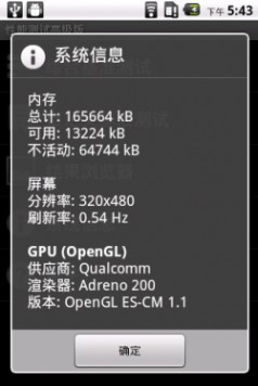
图为:联想A390e手机菜单
通过实际的软件测试之后,最终该机取得了将近600分的成绩,只能说一般般了。具体的硬件配置信息,在图片中也有所展示,就不做叙述。
下面来看一下超级兔子的跑分成绩。

图为:联想A390e手机菜单
最终通过超级兔子测试出的成绩是1447分,表现还是可以接受的。最后再来看一下多点触控方面表现如何。


图为:联想A390e手机菜单
从图片中也可以看到,该机最多支持两点触控,比较遗憾。
总体来说虽然跑分成绩一般,但就操控来说,使用起来并没有明显的卡顿感。所以跑分不过是一种参考标准,用户不必特别在意,真正是用户体验才是王道。
评测总结 拍照效果一般性价比高
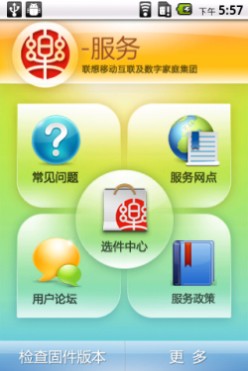
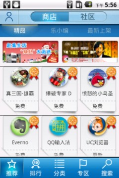
既然是联想推出的产品,自然会内置一些联想的特色软件,如乐服务、乐商店等等,还有电信的互联星空、天翼导航等等。

图为:联想A390e手机菜单
图为:联想A390e手机菜单
这些软件使用起来都比较简单,相信大家也都非常熟悉,所以小编在此就不做过多介绍。下面一起来看看该机320万像素的摄像头拍摄出来的样片到底如何吧。

图为:联想A390e拍照样张

图为:联想A390e拍照样张

图为:联想A390e拍照样张

图为:联想A390e拍照样张
图片中可以看到,北京下雪了。拍照的清晰度方面,320万的像素能达到也还行,不过色彩饱和度方面差了一点。
图为:联想A390e手机
联想A390e让人惊喜的地方:
·外观设计大气、时尚,做工精细
·电信定制,性价比高
·处理器主频达800MHz
·待机能力不错
·内置多款联想实用程序
联想A390e略显不足的地方:
·跑分成绩一般
评测总结:文章看完,大家也可以知道联想A390e是一款入门级的安卓智能机。既然是入门级的产品,作为消费者自然不能将它与高端智能手机相比。而且对于很多学生或者刚入职的白领来说,资金方面并不充裕,所以该机作为中国电信定制产品,在性价比方面还是值得肯定的。
二 : 触摸屏控制方法(转)
最近几天研究了下触摸屏,发现也并不像感觉中的那么神秘。
三 : TSC2046触摸屏控制
TSC 2046TSC2 046TSC2046TSC2 046SBAS265C – OCTOBER 2002 – REVISED JULY 2004Low Voltage I/O TOUCH SCREEN CONTROLLERFEATURESSAME PINOUT AS ADS7846 2.2V TO 5.25V OPERATION 1.5V TO 5.25V DIGITAL I/O INTERNAL 2.5V REFERENCE DIRECT BATTERY MEASUREMENT (0V to 6V) ON-CHIP TEMPERATURE MEASUREMENT TOUCH-PRESSURE MEASUREMENT QSPITM AND SPITM 3-WIRE INTERFACE AUTO POWER-DOWN AVAILABLE IN TSSOP-16, QFN-16, AND VFBGA-48 PACKAGESDESCRIPTIONThe TSC2046 is a next-generation version to the ADS7846 4-wire touch screen controller which supports a low-voltage I/O interface from 1.5V to 5.25V. The TSC2046 is 100% pincompatible with the existing ADS7846, and will drop into the same socket. This allows for easy upgrade of current applications to the new version. The TSC2046 also has an onchip 2.5V reference that can be used for the auxiliary input, battery monitor, and temperature measurement modes. The reference can also be powered down when not used to conserve power. The internal reference operates down to 2.7V supply voltage, while monitoring the battery voltage from 0V to 6V. The low-power consumption of < 0.75mW typ at 2.7V (reference off), high-speed (up to 125kHz sample rate), and onchip drivers make the TSC2046 an ideal choice for batteryoperated systems such as personal digital assistants (PDAs) with resistive touch screens, pagers, cellular phones, and other portable equipment. The TSC2046 is available in TSSOP-16, QFN-16, and VFBGA-48 packages and is specified over the –40°C to +85°C temperature range.APPLICATIONSPERSONAL DIGITAL ASSISTANTS PORTABLE INSTRUMENTS POINT-OF-SALE TERMINALS PAGERS TOUCH SCREEN MONITORS CELLULAR PHONESUS Patent No. 6246394 QSPI and SPI are registered trademarks of Motorola.Pen DetectPENIRQ+VCCX+ X–Temperature SensorSAR IOVDD TSC2046Y+ Y–DOUT BUSYComparator 6-Channel MUX CDAC Serial Data In/Out CSVBAT AUXBattery MonitorDCLK DINVREFInternal 2.5V ReferencePlease be aware that an important notice concerning availability, standard warranty, and use in critical applications of Texas Instruments semiconductor products and disclaimers thereto appears at the end of this data sheet.PRODUCTION DATA information is current as of publication date. Products conform to specifications per the terms of Texas Instruments standard warranty. Production processing does not necessarily include testing of all parameters.Copyright 2002-2004, Texas Instruments Incorporatedwww.ti.com ABSOLUTE MAXIMUM RATINGS(1)+VCC and IOVDD to GND ..................................................... –0.3V to +6V Analog Inputs to GND ............................................ –0.3V to +VCC + 0.3V Digital Inputs to GND .......................................... –0.3V to IOVDD + 0.3V Power Dissipation .......................................................................... 250mW Maximum Junction Temperature ................................................... +150°C Operating Temperature Rang
tsc TSC2046触摸屏控制
e ....................................... –40°C to +85°C Storage Temperature Range ......................................... –65°C to +150°C Lead Temperature (soldering, 10s) ............................................... +300°C NOTE: (1) Stresses above these ratings can cause permanent damage. Exposure to absolute maximum conditions for extended periods may degrade device reliability.ELECTROSTATIC DISCHARGE SENSITIVITYThis integrated circuit can be damaged by ESD. Texas Instruments recommends that all integrated circuits be handled with appropriate precautions. Failure to observe proper handling and installation procedures can cause damage. ESD damage can range from subtle performance degradation to complete device failure. Precision integrated circuits may be more susceptible to damage because very small parametric changes could cause the device not to meet its published specifications.PACKAGE/ORDERING INFORMATION(1)NOMINAL PENIRQ PULLUP RESISTOR VALUES 50k 90k 50k MAXIMUM INTEGRAL LINEARITY PACKAGE ERROR (LSB) PACKAGE-LEAD DESIGNATOR ±2 ±2 ±2 VFBGA-48 VFBGA-48 TSSOP-16 GQC GQC PWPRODUCT TSC2046 TSC2046-90 TSC2046SPECIFIED TEMPERATURE RANGE –40°C to +85°C –40°C to +85°C –40°C to +85°CPACKAGE MARKING AZ2046 AZ2046A TSC2046IORDERING NUMBER TSC2046IGQCR TSC2046IGQCR-90 TSC2046IPW TSC2046IPWR TSC2046IRGVT TSC2046IRGVRTRANSPORT MEDIA, QUANTITY Tape and Reel, 2500 Tape and Reel, 2500 Rails, 100 Tape and Reel, 2500 Tape and Reel, 250 Tape and Reel, 2500"TSC2046"50k"±2"QFN-16"RGV"–40°C to +85°C"TSC2046"""""""NOTE: (1) For the most current specifications and package information, see the Package Option Addendum located at the end of this data sheet.2TSC2046www.ti.comSBAS265C ELECTRICAL CHARACTERISTICSAt TA = –40°C to +85°C, +VCC = +2.7V, VREF = 2.5V internal voltage, fSAMPLE = 125kHz, fCLK = 16 fSAMPLE = 2MHz, 12-bit mode, digital inputs = GND or IOVDD, and +VCC must be IOVDD, unless otherwise noted. TSC2046 PARAMETER ANALOG INPUT Full-Scale Input Span Absolute Input Range Capacitance Leakage Current SYSTEM PERFORMANCE Resolution No Missing Codes Integral Linearity Error Offset Error Gain Error Noise Power-Supply Rejection SAMPLING DYNAMICS Conversion Time Acquisition Time Throughput Rate Multiplexer Settling Time Aperture Delay Aperture Jitter Channel-to-Channel Isolation SWITCH DRIVERS On-Resistance Y+, X+ Y–, X– Drive Current(2) REFERENCE OUTPUT Internal Reference Voltage Internal Reference Drift Quiescent Current REFERENCE INPUT Range Input Impedance CONDITIONS Positive Input-Negative Input Positive Input Negative Input MIN 0 –0.2 –0.2 25 0.1 12 11 ±2 ±6 ±4 70 70 12 3 125 500 30 100 100 TYP MAX VREF +VCC + 0.2 +0.2 UNITS V V V pF A Bits Bits LSB(1) LSB LSB Vrms dB CLK Cycles CLK Cycles kHz ns ns ps dBExternal VREF Including Internal VREFVIN = 2.5Vp-p at 50kHz5 6 Duration 100ms 2.45 2.50 15 500 50 2.55 mA V ppm/°C A V G 1.0 SER/DFR
扩展:tsc2046 / tsc2046中文资料 / tsc2046的中文资料pdf
tsc TSC2046触摸屏控制
= 0, PD1 = 0, Internal Reference Off Internal Reference On 0.5 10 1 VBAT = 0.5V to 5.5V, External VREF = 2.5V VBAT = 0.5V to 5.5V, Internal Reference –2 –3 –40°C Differential Method(3) TEMP0(4) Differential Method(3) TEMP0(4) 1.6 0.3 ±2 ±3 CMOS | IIH | ≤ +5A | IIL | ≤ +5A IOH = –250A IOL = 250A IOVDD 0.7 –0.3 IOVDD 0.8 Straight Binary Specified Performance Operating Range Internal Reference Off Internal Reference On fSAMPLE = 12.5kHz Power-Down Mode with CS = DCLK = DIN = IOVDD +VCC = +2.7V –40 2.7 2.2 1.5 280 780 220 1 250+VCCBATTERY MONITOR Input Voltage Range Input Impedance Sampling Battery Battery Monitor Off Accuracy TEMPERATURE MEASUREMENT Temperature Range Resolution Accuracy DIGITAL INPUT/OUTPUT Logic Family VIH VIL VOH VOL Data Format POWER-SUPPLY REQUIREMENTS +VCC(5) IOVDD(6) Quiescent Current(7)6.0V k G % % °C °C °C °C °C+2 +3 +85IOVDD + 0.3 0.3 IOVDD 0.4V V V V3.6 5.25 +VCC 6503 1.8 +85V V V A A A A mW °CPower Dissipation TEMPERATURE RANGE Specified PerformanceNOTES: (1) LSB means least significant bit. With VREF = +2.5V, one LSB is 610V. (2) Assured by design, but not tested. Exceeding 50mA source current may result in device degradation. (3) Difference between TEMP0 and TEMP1 measurement, no calibration necessary. (4) Temperature drift is –2.1mV/°C. (5) TSC2046 operates down to 2.2V. (6) IOVDD must be - +VCC. (7) Combined supply current from +VCC and IOVDD. Typical values obtained from conversions on AUX input with PD0 = 0.TSC2046SBAS265Cwww.ti.com3 PIN CONFIGURATIONTop View TSSOP Top ViewDCLK CS DIN BUSY DOUTVFBGA+VCC X+ Y+ X– Y– GND VBAT AUX1 2 3 4 5 6 7 8 TSC204616 15 14 13 12 11 10 9DCLK CS DIN BUSY+VCC B NC NC NC NC NC PENIRQ C +VCC D NC NC NC NC NC VREF E Y+ F NC NC NC NC NC NC NC NC NC NC NC NC AUX X+ NC NC NC NC IOVDD 1 A NC 2 3 4 5 6 7 NCDOUT PENIRQ IOVDD VREFG NCNCX–Y–GNDGNDVBATTop View 15 PENIRQTSSOP14 IOVDD16 DOUTBUSY DIN CS DCLK1 2 TSC2046 3 413 VREF12 11 10 9AUX VBAT GND Y–567 Y++VCCX+PIN DESCRIPTIONTSSOP PIN # 1 2 3 4 5 6 7 8 9 10 11 12 13 14 15 16 VFBGA PIN # B1 and C1 D1 E1 G2 G3 G4 and G5 G6 E7 D7 C7 B7 A6 A5 A4 A3 A2 QFN PIN # 5 6 7 8 9 10 11 12 13 14 15 16 1 2 3 4 NAME +VCC X+ Y+ X– Y– GND VBAT AUX VREF IOVDD PENIRQ DOUT BUSY DIN CS DCLK DESCRIPTION Power Supply X+ Position Input Y+ Position Input X– Position Input Y– Position Input Ground Battery Monitor Input Auxiliary Input to ADC Voltage Reference Input/Output Digital I/O Power Supply Pen Interrupt Serial Data Output. Data is shifted on the falling edge of DCLK. This output is high impedance when CS is high. Busy Output. This output is high impedance when CS is high. Serial Data Input. If CS is low, data is latched on rising edge of DCLK. Chip Select Input. Controls conversion timing and enables the serial input/output register. CS high = power-down mode (ADC only). External Clock Input. This clock runs the SAR conversi
tsc TSC2046触摸屏控制
on process and synchronizes serial data I/O.X–84TSC2046www.ti.comSBAS265C TYPICAL CHARACTERISTICSAt TA = +25°C, +VCC = +2.7V, IOVDD = +1.8V, VREF = External +2.5V, 12-bit mode, PD0 = 0, fSAMPLE = 125kHz, and fCLK = 16 fSAMPLE = 2MHz, unless otherwise noted.+VCC SUPPLY CURRENT vs TEMPERATURE 400 350 300 250 200 150 100 –40 –20 0 20 40 60 80 100 Temperature (°C) 30IOVDD SUPPLY CURRENT vs TEMPERATUREIOVDD Supply Current (A)+VCC Supply Current (A)252015105 –40 –20 0 20 40 60 80 100 Temperature (°C)POWER-DOWN SUPPLY CURRENT vs TEMPERATURE 140450 400+VCC Supply Current (A)+VCC SUPPLY CURRENT vs +VCC120Supply Current (nA)fSAMPLE = 125kHz 350 300 250 200 fSAMPLE = 12.5kHz 150 100100806040 –40 –20 0 20 40 60 80 100 Temperature (°C)2.02.53.03.5 +VCC (V)4.04.55.0IOVDD SUPPLY CURRENT vs IOVDD 60 50 40 fSAMPLE = 125kHz 30 20 10 0 1.0 1.5 2.0 2.5 3.0 IOVDD (V) 3.5 4.0 4.5 5.0Sample Rate (Hz)100k 1MMAXIMUM SAMPLE RATE vs +VCC+VCC ≥ IOVDDIOVDD Supply Current (A)10kfSAMPLE = 12.5kHz1k 2.0 2.5 3.0 3.5 +VCC (V) 4.0 4.5 5.0TSC2046SBAS265Cwww.ti.com5 TYPICAL CHARACTERISTICS (Cont.)At TA = +25°C, +VCC = +2.7V, IOVDD = +1.8V, VREF = External +2.5V, 12-bit mode, PD0 = 0, fSAMPLE = 125kHz, and fCLK = 16 fSAMPLE = 2MHz, unless otherwise noted.CHANGE IN GAIN vs TEMPERATURE 0.15 0.10 0.6 0.4CHANGE IN OFFSET vs TEMPERATUREDelta from +25°C (LSB)0.05 0 –0.05 –0.10 –0.15 –40 –20 0 20 40 60 80 100 Temperature (°C)Delta from +25°C (LSB)0.2 0 –0.2 –0.4 –0.6 –40 –20 0 20 40 60 80 100 Temperature (°C)REFERENCE CURRENT vs SAMPLE RATE 14 12 18 16REFERENCE CURRENT vs TEMPERATUREReference Current (A)10 8 6 4 2 0 0 25 50 75 100 125 Sample Rate (kHz)Reference Current (A)14 12 10 8 6 –40 –20 0 20 40 60 80 100 Temperature (°C)SWITCH ON-RESISTANCE vs +VCC (X+, Y+: +VCC to Pin; X–, Y–: Pin to GND) 8SWITCH ON-RESISTANCE vs TEMPERATURE (X+, Y+: +VCC to Pin; X–, Y–: Pin to GND) 8 Y– 77 Y–RON () RON ()6 5 4 3 2 1 X+, Y+ X–65 X+, Y+ 4X–3 2.0 2.5 3.0 3.5 +VCC (V) 4.0 4.5 5.0–40–20020406080100Temperature (°C)6TSC2046www.ti.comSBAS265C TYPICAL CHARACTERISTICS (Cont.)At TA = +25°C, +VCC = +2.7V, IOVDD = +1.8V, VREF = External +2.5V, 12-bit mode, PD0 = 0, fSAMPLE = 125kHz, and fCLK = 16 fSAMPLE = 2MHz, unless otherwise noted.MAXIMUM SAMPLING RATE vs RIN 2.0 Max Absolute Delta Error from RIN = 0 (LSB) 1.8 1.6 1.4 1.2 1.0 0.8 0.6 0.4 0.2 0 20 40 60 80 100 120 140 Sampling Rate (kHz) 160 180 200 INL: RIN = 500 INL: RIN = 2k DNL: RIN = 500 DNL: RIN = 2k2.5080 2.5075 2.5070INTERNAL VREF vs TEMPERATUREInternal VREF (V)2.5065 2.5060 3.5055 2.5050 2.5045 2.5040 2.5035 2.5030INTERNAL VREF vs +VCC 2.510 2.50510080Internal VREF (V)2.500 2.495 2.490 2.485 2.480 2.5 3.0 3.5 4.0 +VCC (V) 4.5 5.0Internal VREF (%)6040200 0 200 400 600 800 1000 1200 1400 Turn-On T
扩展:tsc2046 / tsc2046中文资料 / tsc2046的中文资料pdf
tsc TSC2046触摸屏控制
ime (s)TEMP DIODE VOLTAGE vs TEMPERATURE 850 800TEMP Diode Voltage (mV) 604750 700 650 600 550 500 45090.1mV TEMP1TEMP0 Diode Voltage (mV)602600598TEMP0135.1mV596594 –40 –35 –30 –25 –20 –15 –10 –5 0 5 10 15 20 25 30 35 40 45 50 55 60 65 70 75 80 85 2.7 3.0 +VCC (V) 3.3Temperature (°C)TSC2046SBAS265C–40 –35 –30 –25 –20 –15 –10 –5 0 5 10 15 20 25 30 35 40 45 50 55 60 65 70 75 80 85Temperature (°C)INTERNAL VREF vs TURN-ON TIME No Cap (42s) 12-Bit Settling 1F Cap (1240s) 12-Bit SettlingTEMP0 DIODE VOLTAGE vs +VCCwww.ti.com7 TYPICAL CHARACTERISTICS (Cont.)At TA = +25°C, +VCC = +2.7V, IOVDD = +1.8V, VREF = External +2.5V, 12-bit mode, PD0 = 0, fSAMPLE = 125kHz, and fCLK = 16 fSAMPLE = 2MHz, unless otherwise noted.TEMP1 DIODE VOLTAGE vs +VCC 720TEMP1 Diode Voltage (mV)718716714712710 2.7 3.0 +VCC (V) 3.3THEORY OF OPERATIONThe TSC2046 is a classic successive approximation register (SAR) analog-to-digital converter (ADC). The architecture is based on capacitive redistribution, which inherently includes a sample-and-hold function. The converter is fabricated on a 0.6m CMOS process. The basic operation of the TSC2046 is shown in Figure 1. The device features an internal 2.5V reference and uses an external clock. Operation is maintained from a single supply of 2.7V to 5.25V. The internal reference can be overdriven with an external, low-impedance source between 1V and+VCC. The value of the reference voltage directly sets the input range of the converter. The analog input (X-, Y-, and Z-Position coordinates, auxiliary input, battery voltage, and chip temperature) to the converter is provided via a multiplexer. A unique configuration of low onresistance touch panel driver switches allows an unselected ADC input channel to provide power and the accompanying pin to provide ground for an external device, such as a touch screen. By maintaining a differential input to the converter and a differential reference architecture, it is possible to negate the error from each touch panel driver switch's on-resistance (if this is a source of error for the particular measurement).+2.7V to +5V 1F + to 10F (Optional)TSC2046 B1 +VCC C1 +VCC D1 X+ E1 Y+ DCLK A2 CS A3 DIN A4 BUSY A5 DOUT A6 PENIRQ B7 IOVDD C7 VREF D7 G5 GND Serial/Conversion Clock Chip Select Serial Data In Converter Status Serial Data Out Pen Interrupt0.1FTouch Screen To BatteryG2 X– G3 Y– G6 VBAT Auxiliary Input E7 AUX GND G4Voltage RegulatorNOTE: BGA package and pin names shown.FIGURE 1. Basic Operation of the TSC2046.8TSC2046www.ti.comSBAS265C ANALOG INPUTFigure 2 shows a block diagram of the input multiplexer on the TSC2046, the differential input of the ADC, and the differential reference of the converter. Table I and Table II show the relationship between the A2, A1, A0, and SER/DFR control bits and the configuration of the TSC2046. The control bits are provided serially via the DIN
tsc TSC2046触摸屏控制
pin—see the Digital Interface section of this data sheet for more details.When the converter enters the hold mode, the voltage difference between the +IN and –IN inputs (as shown in Figure 2) is captured on the internal capacitor array. The input current into the analog inputs depends on the conversion rate of the device. During the sample period, the source must charge the internal sampling capacitor (typically 25pF). After the capacitor has been fully charged, there is no further input current. The rate of charge transfer from the analog source to the converter is a function of conversion rate.PENIRQIOVDD TEMP1 50k or 90k TEMP0+VCCVREFLevel ShifterLogicA2-A0 (Shown 001B)SER/DFR (Shown Low)X+ X– Ref On/Off Y+ Y– 2.5V Reference +REF ADC –IN –REF+IN7.5k VBAT 2.5kAUX GNDBattery OnFIGURE 2. Simplified Diagram of Analog Input.A2 0 0 0 0 1 1 1 1 A1 0 0 1 1 0 0 1 1 A0 0 1 0 1 0 1 0 1 VBAT AUXIN TEMP +IN (TEMP0) +IN +IN +IN +IN +IN +IN +IN (TEMP1) Measure Measure Measure Measure Y– X+ Y+ Y-POSITION X-POSITION Z1-POSITION Z2-POSITION X-DRIVERS Off Off Off X–, On X–, On On Off Off Y-DRIVERS Off On Off Y+, On Y+, On Off Off OffTABLE I. Input Configuration (DIN), Single-Ended Reference Mode (SER/DFR high).A2 0 0 1 1 A1 0 1 0 0 A0 1 1 0 1 +REF Y+ Y+ Y+ X+ –REF Y– X– X– X– Y– X+ +IN +IN +IN +IN Measure Y+ Y-POSITION Measure Measure Measure X-POSITION Z1-POSITION Z2-POSITION DRIVERS ON Y+, Y+, Y+, X+, Y– X– X– X–TABLE II. Input Configuration (DIN), Differential Reference Mode (SER/DFR low).TSC2046SBAS265Cwww.ti.com9 INTERNAL REFERENCEThe TSC2046 has an internal 2.5V voltage reference that can be turned on or off with the control bit, PD1 (see Table V and Figure 3). Typically, the internal reference voltage is only used in the single-ended mode for battery monitoring, temperature measurement, and for using the auxiliary input. Optimal touch screen performance is achieved when using the differential mode. The internal reference voltage of the TSC2046 must be commanded to be off to maintain compatibility with the ADS7843. Therefore, after power-up, a write of PD1 = 0 is required to insure the reference is off (see the Typical Characteristics for power-up time of the reference from powerdown).is made by connecting the X+ input to the ADC, turning on the Y+ and Y– drivers, and digitizing the voltage on X+ (Figure 4 shows a block diagram). For this measurement, the resistance in the X+ lead does not affect the conversion (it does affect the settling time, but the resistance is usually small enough that this is not a concern). However, since the resistance between Y+ and Y– is fairly low, the on-resistance of the Y drivers does make a small difference. Under the situation outlined so far, it is not possible to achieve a 0V input or a full-scale input regardless of where the pointing device is on the touch screen because some voltage is lost across the internal switches. In addit
扩展:tsc2046 / tsc2046中文资料 / tsc2046的中文资料pdf
tsc TSC2046触摸屏控制
ion, the internal switch resistance is unlikely to track the resistance of the touch screen, providing an additional source of error.Reference Power-Down+VCCVREFY+Band GapVREF BufferX+ +IN –IN +REF Converter –REFTo CDACOptionalY–FIGURE 3. Simplified Diagram of the Internal Reference.REFERENCE INPUTThe voltage difference between +REF and –REF (see Figure 2) sets the analog input range. The TSC2046 operates with a reference in the range of 1V to +VCC. There are several critical items concerning the reference input and its wide voltage range. As the reference voltage is reduced, the analog voltage weight of each digital output code is also reduced. This is often referred to as the LSB (least significant bit) size and is equal to the reference voltage divided by 4096 in 12-bit mode. Any offset or gain error inherent in the ADC appears to increase, in terms of LSB size, as the reference voltage is reduced. For example, if the offset of a given converter is 2LSBs with a 2.5V reference, it is typically 5LSBs with a 1V reference. In each case, the actual offset of the device is the same, 1.22mV. With a lower reference voltage, more care must be taken to provide a clean layout including adequate bypassing, a clean (low-noise, lowripple) power supply, a low-noise reference (if an external reference is used), and a low-noise input signal. The voltage into the VREF input directly drives the capacitor digital-to-analog converter (CDAC) portion of the TSC2046. Therefore, the input current is very low (typically < 13A). There is also a critical item regarding the reference when making measurements while the switch drivers are ON. For this discussion, it is useful to consider the basic operation of the TSC2046, (see Figure 1). This particular application shows the device being used to digitize a resistive touch screen. A measurement of the current Y-Position of the pointing deviceGNDFIGURE 4. Simplified Diagram of Single-Ended Reference (SER/DFR high, Y switches enabled, X+ is analog input). This situation can be remedied as shown in Figure 5. By setting the SER/DFR bit low, the +REF and –REF inputs are connected directly to Y+ and Y–, respectively, which makes the analog-todigital conversion ratiometric. The result of the conversion is+VCCY+X++IN –IN+REF Converter –REFY–GNDFIGURE 5. Simplified Diagram of Differential Reference (SER/DFR low, Y switches enabled, X+ is analog input).10TSC2046www.ti.comSBAS265C always a percentage of the external resistance, regardless of how it changes in relation to the on-resistance of the internal switches. Note that there is an important consideration regarding power dissipation when using the ratiometric mode of operation (see the Power Dissipation section for more details). As a final note about the differential reference mode, it must be used with +VCC as the source of the +REF voltage and cannot be used with VREF. It is possible to use a highprecision re
tsc TSC2046触摸屏控制
ference on VREF and single-ended reference mode for measurements which do not need to be ratiometric. In some cases, it is possible to power the converter directly from a precision reference. Most references can provide enough power for the TSC2046, but might not be able to supply enough current for the external load (such as a resistive touch screen).offers two modes of operation. The first mode requires calibration at a known temperature, but only requires a single reading to predict the ambient temperature. A diode is used (turned on) during this measurement cycle. The voltage across the diode is connected through the MUX for digitizing the forward bias voltage by the ADC with an address of A2 = 0, A1 = 0, and A0 = 0 (see Table I and Figure 6 for details). This voltage is typically 600mV at +25°C with a 20A current through the diode. The absolute value of this diode voltage can vary a few millivolts. However, the TC of this voltage is very consistent at –2.1mV/°C. During the final test of the end product, the diode voltage would be stored at a known room temperature, in memory, for calibration purposes by the user. The result is an equivalent temperature measurement resolution of 0.3°C/LSB (in 12-bit mode).TOUCH SCREEN SETTLINGIn some applications, external capacitors may be required across the touch screen for filtering noise picked up by the touch screen (e.g., noise generated by the LCD panel or backlight circuitry). These capacitors provide a low-pass filter to reduce the noise, but cause a settling time requirement when the panel is touched that typically shows up as a gain error. There are several methods for minimizing or eliminating this issue. The problem is the input and/or reference has not settled to the final steady-state value prior to the ADC sampling the input(s) and providing the digital output. Additionally, the reference voltage may still be changing during the measurement cycle. Option 1 is to stop or slow down the TSC2046 DCLK for the required touch screen settling time. This allows the input and reference to have stable values for the Acquire period (3 clock cycles of the TSC2046; see Figure 9). This works for both the single-ended and the differential modes. Option 2 is to operate the TSC2046 in the differential mode only for the touch screen measurements and command the TSC2046 to remain on (touch screen drivers ON) and not go into power-down (PD0 = 1). Several conversions are made depending on the settling time required and the TSC2046 data rate. Once the required number of conversions have been made, the processor commands the TSC2046 to go into its power-down state on the last measurement. This process is required for X-Position, Y-Position, and Z-Position measurements. Option 3 is to operate in the 15 Clock-per-Conversion mode, which overlaps the analog-to-digital conversions and maintains the touch screen drivers on until commanded to stop by the processor (see Figure 13).+VCCTEMP0TEMP1MUXADCF
扩展:tsc2046 / tsc2046中文资料 / tsc2046的中文资料pdf
tsc TSC2046触摸屏控制
IGURE 6. Functional Block Diagram of Temperature Measurement Mode. The second mode does not require a test temperature calibration, but uses a two-measurement method to eliminate the need for absolute temperature calibration and for achieving 2°C accuracy. This mode requires a second conversion with an address of A2 = 1, A1 = 1, and A0 = 1, with a 91 times larger current. The voltage difference between the first and second conversion using 91 times the bias current is represented by kT/q ln (N), where N is the current ratio = 91, k = Boltzmann's constant (1.38054 10–23 electron volts/ degrees Kelvin), q = the electron charge (1.602189 10–19 C), and T = the temperature in degrees Kelvin. This method can provide improved absolute temperature measurement over the first mode at the cost of less resolution (1.6°C/LSB). The equation for solving for °K is: °K = q V/(k ln (N)) where, V = V (I91) – V (I1) (in mV) ∴ °K = 2.573 °K/mV V °C = 2.573 V(mV) – 273°K NOTE: The bias current for each diode temperature measurement is only on for 3 clock cycles (during the acquisition mode) and, therefore, does not add any noticeable increase in power, especially if the temperature measurement only occurs occasionally. (1)TEMPERATURE MEASUREMENTIn some applications, such as battery recharging, a measurement of ambient temperature is required. The temperature measurement technique used in the TSC2046 relies on the characteristics of a semiconductor junction operating at a fixed current level. The forward diode voltage (VBE) has a well-defined characteristic versus temperature. The ambient temperature can be predicted in applications by knowing the +25°C value of the VBE voltage and then monitoring the delta of that voltage as the temperature changes. The TSC2046TSC2046SBAS265Cwww.ti.com11 BATTERY MEASUREMENTAn added feature of the TSC2046 is the ability to monitor the battery voltage on the other side of the voltage regulator (DC/DC converter), as shown in Figure 7. The battery voltage can vary from 0V to 6V, while maintaining the voltage to the TSC2046 at 2.7V, 3.3V, etc. The input voltage (VBAT) is divided down by 4 so that a 5.5V battery voltage is represented as 1.375V to the ADC. This simplifies the multiplexer and control logic. In order to minimize the power consumption, the divider is only on during the sampling period when A2 = 0, A1 = 1, and A0 = 0 (see Table I for the relationship between the control bits and configuration of the TSC2046).Measure X-Position X+ Touch Y+X-Position X– Y–Measure Z1-Position X+ Touch Y+DC/DC Converter Battery 0.5V to 5.5V+2.7VZ1-Position X– Y–+VCCX+ TouchY+0.125V to 1.375V VBAT 7.5kX–ADCZ2-Position Y– Measure Z2-Position2.5kFIGURE 8. Pressure Measurement Block Diagrams. FIGURE 7. Battery Measurement Functional Block Diagram.DIGITAL INTERFACESee Figure 9 for the typical operation of the TSC2046 digital interface. This diagram assumes that the source o
tsc TSC2046触摸屏控制
f the digital signals is a microcontroller or digital signal processor with a basic serial interface. Each communication between the processor and the converter, such as SPI, SSI, or Microwire synchronous serial interface, consists of eight clock cycles. One complete conversion can be accomplished with three serial communications for a total of 24 clock cycles on the DCLK input. The first eight clock cycles are used to provide the control byte via the DIN pin. When the converter has enough information about the following conversion to set the input multiplexer and reference inputs appropriately, the converter enters the acquisition (sample) mode and, if needed, the touch panel drivers are turned on. After three more clock cycles, the control byte is complete and the converter enters the conversion mode. At this point, the input sample-andhold goes into the hold mode and the touch panel drivers turn off (in single-ended mode). The next 12 clock cycles accomplish the actual analog-to-digital conversion. If the conversion is ratiometric (SER/DFR = 0), the drivers are on during the conversion and a 13th clock cycle is needed for the last bit of the conversion result. Three more clock cycles are needed to complete the last byte (DOUT will be low), which are ignored by the converter.Microwire is a registered trademark of National Semiconductor.PRESSURE MEASUREMENTMeasuring touch pressure can also be done with the TSC2046. To determine pen or finger touch, the pressure of the touch needs to be determined. Generally, it is not necessary to have very high performance for this test, therefore, the 8-bit resolution mode is recommended (however, calculations will be shown here in the 12-bit resolution mode). There are several different ways of performing this measurement. The TSC2046 supports two methods. The first method requires knowing the X-plate resistance, measurement of the X-Position, and two additional cross panel measurements (Z1 and Z2) of the touch screen, as shown in Figure 8. Using Equation 2 calculates the touch resistance:R TOUCH = R X– plate X – Position Z 2 –1 Z1 4096 (2)The second method requires knowing both the X-plate and Y-plate resistance, measurement of X-Position and Y-Position, and Z1. Using Equation 3 also calculates the touch resistance:RTOUCH =R Xplate X Position 4096 –1 Z1 4096(3)Y Position – R Yplate 1 409612TSC2046www.ti.comSBAS265C Control ByteThe control byte (on DIN), as shown in Table III, provides the start conversion, addressing, ADC resolution, configuration, and power-down of the TSC2046. Figure 9 and Tables III and IV give detailed information regarding the order and description of these control bits within the control byte.Bit 7 (MSB) S Bit 0 (LSB) PD0MODE—The mode bit sets the resolution of the ADC. With this bit low, the next conversion has 12 bits of resolution, whereas with this bit high, the next conversion has 8 bits of resolution.SER/DFR—The SER/DF
扩展:tsc2046 / tsc2046中文资料 / tsc2046的中文资料pdf
tsc TSC2046触摸屏控制
R bit controls the reference mode, either single-ended (high) or differential (low). The differential mode is also referred to as the ratiometric conversion mode and is preferred for X-Position, Y-Position, and PressureTouch measurements for optimum performance. The reference is derived from the voltage at the switch drivers, which is almost the same as the voltage to the touch screen. In this case, a reference voltage is not needed as the reference voltage to the ADC is the voltage across the touch screen. In the single-ended mode, the converter reference voltage is always the difference between the VREF and GND pins (see Tables I and II, and Figures 2 through 5 for further information).Bit 6 A2Bit 5 A1Bit 4 A0Bit 3Bit 2Bit 1 PD1MODE SER/DFRTABLE III. Order of the Control Bits in the Control Byte.BIT 7 NAME S DESCRIPTION Start bit. Control byte starts with first high bit on DIN. A new control byte can start every 15th clock cycle in 12-bit conversion mode or every 11th clock cycle in 8-bit conversion mode (see Figure 13). Channel Select bits. Along with the SER/DFR bit, these bits control the setting of the multiplexer input, touch driver switches, and reference inputs (see Tables I and II). 12-Bit/8-Bit Conversion Select bit. This bit controls the number of bits for the next conversion: 12-bits (low) or 8-bits (high). Single-Ended/Differential Reference Select bit. Along with bits A2-A0, this bit controls the setting of the multiplexer input, touch driver switches, and reference inputs (see Tables I and II). Power-Down Mode Select bits. Refer to Table V for details.6-4A2-A03MODE2SER/DFRIf X-Position, Y-Position, and Pressure-Touch are measured in the single-ended mode, an external reference voltage is needed. The TSC2046 must also be powered from the external reference. Caution should be observed when using the single-ended mode such that the input voltage to the ADC does not exceed the internal reference voltage, especially if the supply voltage is greater than 2.7V. NOTE: The differential mode can only be used for X-Position, Y-Position, and Pressure-Touch measurements. All other measurements require the single-ended mode. PD0 and PD1—Table V describes the power-down and the internal reference voltage configurations. The internal reference voltage can be turned on or off independently of the ADC. This can allow extra time for the internal reference voltage to settle to the final value prior to making a conversion. Make sure to also allow this extra wake-up time if the internal reference is powered down. The ADC requires no wake-up time and can be instantaneously used. Also note1-0PD1-PD0TABLE IV. Descriptions of the Control Bits within the Control Byte. Initiate START—The first bit, the S bit, must always be high and initiates the start of the control byte. The TSC2046 ignores inputs on the DIN pin until the start bit is detected. Addressing—The next three bits (A2, A1, and A0) select the active inpu
tsc TSC2046触摸屏控制
t channel(s) of the input multiplexer (see Tables I, II, and Figure 2), touch screen drivers, and the reference inputs.CStACQDCLK DIN1SER/81818SA2A1 IdleA0 MODE DFR PD1 PD0 Acquire Conversion Idle(START)BUSY DOUT Drivers 1 and 2(1) (SER/DFR High) Drivers 1 and 2(1, 2) (SER/DFR Low)11 (MSB) Off On Off 10 9 8 7 6 5 4 3 2 1 0 (LSB) Zero Filled...OffOnOffNOTES: (1) For Y-Position, Driver 1 is on X+ is selected, and Driver 2 is off. For X-Position, Driver 1 is off, Y+ is selected, and Driver 2 is on. Y– will turn on when power-down mode is entered and PD0 = 0. (2) Drivers will remain on if PD0 = 1 (no power down) until selected input channel, reference mode, or power-down mode is changed, or CS is high.FIGURE 9. Conversion Timing, 24 Clocks-per-Conversion, 8-Bit Bus Interface. No DCLK delay required with dedicated serial port.TSC2046SBAS265Cwww.ti.com13 PD1 0PD0 0PENIRQ EnabledDESCRIPTION Power-Down Between Conversions. When each conversion is finished, the converter enters a low-power mode. At the start of the next conversion, the device instantly powers up to full power. There is no need for additional delays to ensure full operation, and the very first conversion is valid. The Y– switch is on when in power-down. Reference is off and ADC is on. Reference is on and ADC is off. Device is always powered. Reference is on and ADC is ON.X+ Y+ High except when TEMP0, TEMP1 activated. TEMP DIODE IOVDD+VCC 50k or 90kLevel ShifterPENIRQ+VCC TEMP0 TEMP10 1 11 0 1Disabled Enabled DisabledTABLE V. Power-Down and Internal Reference Selection. that the status of the internal reference power-down is latched into the part (internally) with BUSY going high. In order to turn the reference off, an additional write to the TSC2046 is required after the channel has been converted.Y– On Y+ or X+ drivers on, or TEMP0, TEMP1 measurements activated.PENIRQ OUTPUTThe pen-interrupt output function is shown in Figure 10. While in power-down mode with PD0 = 0, the Y– driver is on and connects the Y-plane of the touch screen to GND. The PENIRQ output is connected to the X+ input through two transmission gates. When the screen is touched, the X+ input is pulled to ground through the touch screen. In most of the TSC2046 models, the internal pullup resistor value is nominally 50k, but this may vary between 36k and 67k given process and temperature variations. In order to assure a logic low of 0.35VDD is presented to the PENIRQ circuitry, the total resistance between the X+ and Y- terminals must be less than 21k. The -90 version of the TSC2046 uses a nominal 90k pullup resistor, which allows the total resistance between the X+ and Y- terminals to be as high as 30k. Note that the higher pullup resistance will cause a slower response time of the PENIRQ to a screen touch, so user software should take this into account. The PENIRQ output goes low due to the current path through the touch screen to ground,
扩展:tsc2046 / tsc2046中文资料 / tsc2046的中文资料pdf
tsc TSC2046触摸屏控制
which initiates an interrupt to the FIGURE 10. PENIRQ Functional Block Diagram. processor. During the measurement cycle for X-, Y-, and ZPosition, the X+ input is disconnected from the PENIRQ internal pull-up resistor. This is done to eliminate any leakage current from the internal pull-up resistor through the touch screen, thus causing no errors. Furthermore, the PENIRQ output is disabled and low during the measurement cycle for X-, Y-, and Z-Position. The PENIRQ output is disabled and high during the measurement cycle for battery monitor, auxiliary input, and chip temperature. If the last control byte written to the TSC2046 contains PD0 = 1, the pen-interrupt output function is disabled and is not able to detect when the screen is touched. In order to re-enable the pen-interrupt output function under these circumstances, a control byte needs to be written to the TSC2046 with PD0 = 0. If the last control byte written to the TSC2046 contains PD0 = 0, the pen-interrupt output function is enabled at the end of the conversion. The end of the conversion occurs on the falling edge of DCLK after bit 1 of the converted data isCSDCLK1 8 1 8 1 8 1DINS Control BitsS Control BitsBUSYDOUT11 10 987654321011 10 9FIGURE 11. Conversion Timing, 16 Clocks-per-Conversion, 8-Bit Bus Interface. No DCLK delay required with dedicated serial port.14TSC2046www.ti.comSBAS265C clocked out of the TSC2046. It is recommended that the processor mask the interrupt PENIRQ is associated with whenever the processor sends a control byte to the TSC2046. This prevents false triggering of interrupts when the PENIRQ output is disabled in the cases discussed in this section.+VCC 2.7V, +VCC IOVDD 1.5V, CLOAD = 50pF SYMBOL tACQ tDS tDH tDO tDV tTR tCSS tCSH tCH tCL tBD tBDV tBTR DESCRIPTION Acquisition Time DIN Valid Prior to DCLK Rising DIN Hold After DCLK High DCLK Falling to DOUT Valid CS Falling to DOUT Enabled CS Rising to DOUT Disabled CS Falling to First DCLK Rising CS Rising to DCLK Ignored DCLK High DCLK Low DCLK Falling to BUSY Rising/Falling CS Falling to BUSY Enabled CS Rising to BUSY Disabled 100 10 200 200 200 200 200 MIN 1.5 100 50 200 200 200 TYP MAX UNITS s ns ns ns ns ns ns ns ns ns ns ns ns16 Clocks-per-ConversionThe control bits for conversion n + 1 can be overlapped with conversion n to allow for a conversion every 16 clock cycles, as shown in Figure 11. This figure also shows possible serial communication occurring with other serial peripherals between each byte transfer from the processor to the converter. This is possible, provided that each conversion completes within 1.6ms of starting. Otherwise, the signal that is captured on the input sample-and-hold may droop enough to affect the conversion result. Note that the TSC2046 is fully powered while other serial communications are taking place during a conversion.TABLE VI. Timing Specifications, TA = –40°C to +85°C.CS tCSS DCLK tDS DIN tBDV BUSY tDV DOUT
tsc TSC2046触摸屏控制
11 10 tTR tDH PD0 tBTR tCH tCL tBD tBD tDO tCSHFIGURE 12. Detailed Timing Diagram.CSPower-DownDCLK 1SER/151SER/151DINSA2 A1 A0 MODE DFR PD1 PD0SA2 A1 A0 MODE DFR PD1 PD0SA2A1 A0BUSYDOUT11 10987654321011 10987FIGURE 13. Maximum Conversion Rate, 15 Clocks-per-Conversion.TSC2046SBAS265Cwww.ti.com15 Digital TimingFigures 9 and 12 and Table VI provide detailed timing for the digital interface of the TSC2046.POWER DISSIPATIONThere are two major power modes for the TSC2046: full-power (PD0 = 1) and auto power-down (PD0 = 0). When operating at full speed and 16 clocks-per-conversion (see Figure 11), the TSC2046 spends most of the time acquiring or converting. There is little time for auto power-down, assuming that this mode is active. Therefore, the difference between full-power mode and auto power-down is negligible. If the conversion rate15 Clocks-per-ConversionFS = Full-Scale Voltage = VREF(1) 1LSB = VREF(1)/4096 1LSB 11...111100011...110Output Code11...101fCLK = 16 fSAMPLESupply Current (A)100 fCLK = 2MHz 1000...010 00...001 00...000Supply Current from +VCC and IOVDD TA = 25°C +VCC = 2.7V IOVDD = 1.8V0V Input Voltage(2) (V)FS – 1LSB1NOTES: (1) Reference voltage at converter: +REF – (–REF), see Figure 2. (2) Input voltage at converter, after multiplexer: +IN – (–IN), see Figure 21k10k fSAMPLE (Hz)100k1MFIGURE 14. Ideal Input Voltages and Output Codes. Figure 13 provides the fastest way to clock the TSC2046. This method does not work with the serial interface of most microcontrollers and digital signal processors, as they are generally not capable of providing 15 clock cycles per serial transfer. However, this method can be used with field programmable gate arrays (FPGAs) or application specific integrated circuits (ASICs). Note that this effectively increases the maximum conversion rate of the converter beyond the values given in the specification tables, which assume 16 clock cycles per conversion. FIGURE 15. Supply Current versus Directly Scaling the Frequency of DCLK with Sample Rate or Maintaining DCLK at the Maximum Possible Frequency.is decreased by slowing the frequency of the DCLK input, the two modes remain approximately equal. However, if the DCLK frequency is kept at the maximum rate during a conversion but conversions are done less often, the difference between the two modes is dramatic. Figure 15 shows the difference between reducing the DCLK frequency (scaling DCLK to match the conversion rate) or maintaining DCLK at the highest frequency and reducing the number of conversions per second. In the latter case, the converter spends an increasing percentage of time in powerdown mode (assuming the auto power-down mode is active). Another important consideration for power dissipation is the reference mode of the converter. In the single-ended reference mode, the touch panel drivers are ON only when the analog
扩展:tsc2046 / tsc2046中文资料 / tsc2046的中文资料pdf
tsc TSC2046触摸屏控制
input voltage is being acquired (see Figure 9 and Table I). The external device (e.g., a resistive touch screen), therefore, is only powered during the acquisition period. In the differential reference mode, the external device must be powered throughout the acquisition and conversion periods (see Figure 9). If the conversion rate is high, this could substantially increase power dissipation.Data FormatThe TSC2046 output data is in Straight Binary format, as shown in Figure 14. This figure shows the ideal output code for the given input voltage and does not include the effects of offset, gain, or noise.8-Bit ConversionThe TSC2046 provides an 8-bit conversion mode that can be used when faster throughput is needed and the digital result is not as critical. By switching to the 8-bit mode, a conversion is complete four clock cycles earlier. Not only does this shorten each conversion by four bits (25% faster throughput), but each conversion can actually occur at a faster clock rate. This is because the internal settling time of the TSC2046 is not as critical—settling to better than 8 bits is all that is needed. The clock rate can be as much as 50% faster. The faster clock rate and fewer clock cycles combine to provide a 2x increase in conversion rate.16TSC2046www.ti.comSBAS265C CS also puts the TSC2046 into power-down mode. When CS goes high, the TSC2046 immediately goes into powerdown mode and does not complete the current conversion. The internal reference, however, does not turn off with CS going high. To turn the reference off, an additional write is required before CS goes high (PD1 = 0). When the TSC2046 first powers up, the device draws about 20A of current until a control byte is written to it with PD0 = 0 to put it into power-down mode. This can be avoided if the TSC2046 is powered up with CS = 0 and DCLK = IOVDD.power dissipation through the bypass capacitors when the TSC2046 is in power-down mode. A bypass capacitor is generally not needed on the VREF pin because the internal reference is buffered by an internal op amp. If an external reference voltage originates from an op amp, make sure that it can drive any bypass capacitor that is used without oscillation. The TSC2046 architecture offers no inherent rejection of noise or voltage variation in regards to using an external reference input. This is of particular concern when the reference input is tied to the power supply. Any noise and ripple from the supply appears directly in the digital results. Whereas high-frequency noise can be filtered out, voltage variation due to line frequency (50Hz or 60Hz) can be difficult to remove. The GND pin must be connected to a clean ground point. In many cases, this is the analog ground. Avoid connections which are too near the grounding point of a microcontroller or digital signal processor. If needed, run a ground trace directly from the converter to the power-supply entry or batteryconnection point. The ideal layout includes an analo
tsc TSC2046触摸屏控制
g ground plane dedicated to the converter and associated analog circuitry. In the specific case of use with a resistive touch screen, care should be taken with the connection between the converter and the touch screen. Although resistive touch screens have fairly low resistance, the interconnection should be as short and robust as possible. Longer connections are a source of error, much like the on-resistance of the internal switches. Likewise, loose connections can be a source of error when the contact resistance changes with flexing or vibrations. As indicated previously, noise can be a major source of error in touch screen applications (e.g., applications that require a backlit LCD panel). This EMI noise can be coupled through the LCD panel to the touch screen and cause "flickering" of the converted data. Several things can be done to reduce this error, such as using a touch screen with a bottom-side metal layer connected to ground to shunt the majority of noise to ground. Additionally, filtering capacitors from Y+, Y–, X+, and X– pins to ground can also help. Caution should be observed under these circumstances for settling time of the touch screen, especially operating in the single-ended mode and at high data rates.LAYOUTThe following layout suggestions provide the most optimum performance from the TSC2046. Many portable applications, however, have conflicting requirements concerning power, cost, size, and weight. In general, most portable devices have fairly clean power and grounds because most of the internal components are very low power. This situation means less bypassing for the converter power and less concern regarding grounding. Still, each situation is unique and the following suggestions should be reviewed carefully. For optimum performance, care should be taken with the physical layout of the TSC2046 circuitry. The basic SAR architecture is sensitive to glitches or sudden changes on the power supply, reference, ground connections, and digital inputs that occur just prior to latching the output of the analog comparator. Therefore, during any single conversion for an n-bitSAR converter, there are n 'windows' in which large external transient voltages can easily affect the conversion result. Such glitches can originate from switching power supplies, nearby digital logic, and high-power devices. The degree of error in the digital output depends on the reference voltage, layout, and the exact timing of the external event. The error can change if the external event changes in time with respect to the DCLK input. With this in mind, power to the TSC2046 should be clean and well bypassed. A 0.1F ceramic bypass capacitor should be placed as close to the device as possible. A 1F to 10F capacitor may also be needed if the impedance of the connection between +VCC or IOVDD and the power supplies is high. Low-leakage capacitors should be used to minimizeTSC2046SBAS265Cwww.ti.com17 PACKAGE OPTION ADDENDUMwww.ti.com4-Jan-2005
扩展:tsc2046 / tsc2046中文资料 / tsc2046的中文资料pdf
tsc TSC2046触摸屏控制
PACKAGING INFORMATIONOrderable Device TSC2046EIPW TSC2046EIPWR TSC2046EIZQCR Status (1) PREVIEW PREVIEW PREVIEW Package Type TSSOP TSSOP BGA MI CROSTA R JUNI OR VFBGA TSSOP TSSOP TSSOP QFN QFN QFN BGA MI CROSTA R JUNI OR BGA MI CROSTA R JUNI OR Package Drawing PW PW ZQC Pins Package Eco Plan (2) Qty 16 16 48 90 2000 2500 None None None Lead/Ball Finish Call TI Call TI Call TI MSL Peak Temp (3) Call TI Call TI Call TITSC2046IGQCR TSC2046IPW TSC2046IPWR TSC2046IPWRG4 TSC2046IRGVR TSC2046IRGVRG4 TSC2046IRGVT TSC2046IZQCRACTIVE ACTIVE ACTIVE PREVIEW ACTIVE ACTIVE ACTIVE ACTIVEGQC PW PW PW RGV RGV RGV ZQC48 16 16 16 16 16 16 482500 100 2500None None None Green (RoHS & no Sb/Br)SNPB CU NIPDAU CU NIPDAU CU NIPDAU CU NIPDAU CU NIPDAU CU NIPDAU SNAGCULevel-2A-235C-4 WKS Level-2-220C-1 YEAR Level-2-220C-1 YEAR Level-1-260C-UNLIM Level-1-235C-UNLIM Level-1-260C-UNLIM Level-1-235C-UNLIM Level-3-260C-168 HR2500None2500 Green (RoHS & no Sb/Br) 250 2500 None Pb-Free (RoHS)TSC2046IZQCR-90ACTIVEZQC482500Pb-Free (RoHS)SNAGCULevel-3-260C-168 HR(1)The marketing status values are defined as follows: ACTIVE: Product device recommended for new designs. LIFEBUY: TI has announced that the device will be discontinued, and a lifetime-buy period is in effect. NRND: Not recommended for new designs. Device is in production to support existing customers, but TI does not recommend using this part in a new design. PREVIEW: Device has been announced but is not in production. Samples may or may not be available. OBSOLETE: TI has discontinued the production of the device.(2)Eco Plan - May not be currently available - please check http://www.ti.com/productcontent for the latest availability information and additional product content details. None: Not yet available Lead (Pb-Free). Pb-Free (RoHS): TI's terms "Lead-Free" or "Pb-Free" mean semiconductor products that are compatible with the current RoHS requirements for all 6 substances, including the requirement that lead not exceed 0.1% by weight in homogeneous materials. Where designed to be soldered at high temperatures, TI Pb-Free products are suitable for use in specified lead-free processes. Green (RoHS & no Sb/Br): TI defines "Green" to mean "Pb-Free" and in addition, uses package materials that do not contain halogens, including bromine (Br) or antimony (Sb) above 0.1% of total product weight.(3)MSL, Peak Temp. -- The Moisture Sensitivity Level rating according to the JEDECindustry standard classifications, and peak solder temperature. Important Information and Disclaimer:The information provided on this page represents TI's knowledge and belief as of the date that it is provided. TI bases its knowledge and belief on information provided by third parties, and makes no representation or warranty as to the accuracy of such information. Efforts are underway to better integrate information from third parties. TI has taken and continues to take reasonable steps to provide representa
tsc TSC2046触摸屏控制
tive and accurate information but may not have conducted destructive testing or chemical analysis on incoming materials and chemicals. TI and TI suppliers consider certain information to be proprietary, and thus CAS numbers and other limited information may not be available for release. In no event shall TI's liability arising out of such information exceed the total purchase price of the TI part(s) at issue in this document sold by TI to Customer on an annual basis.Addendum-Page 1 MECHANICAL DATAMPLG008D – APRIL 2000 – REVISED FEBRUARY 2002GQC (S-PBGA-N48)PLASTIC BALL GRID ARRAY4,10 3,90SQ 0,503,00 TYPG F E D C B A 0,50 3,00 TYPA1 Corner1234567Bottom View 0,77 0,71 1,00 MAXSeating Plane 0,35 0,25 0,05 M 0,25 0,150,084200460/E 01/02 NOTES: A. B. C. D. All linear dimensions are in millimeters. This drawing is subject to change without notice. MicroStar Junior BGA configuration Falls within JEDEC MO-225MicroStar Junior is a trademark of Texas Instruments.POST OFFICE BOX 655303 DALLAS, TEXAS 752651 MECHANICAL DATAMTSS001C – JANUARY 1995 – REVISED FEBRUARY 1999PW (R-PDSO-G**)14 PINS SHOWNPLASTIC SMALL-OUTLINE PACKAGE0,65 14 80,30 0,190,10 M0,15 NOM 4,50 4,30 6,60 6,20 Gage Plane 0,25 1 A 7 0°– 8° 0,75 0,50Seating Plane 1,20 MAX 0,15 0,05 0,10PINS ** DIM A MAX814162024283,105,105,106,607,909,80A MIN2,904,904,906,407,709,604040064/F 01/97 NOTES: A. B. C. D. All linear dimensions are in millimeters. This drawing is subject to change without notice. Body dimensions do not include mold flash or protrusion not to exceed 0,15. Falls within JEDEC MO-153POST OFFICE BOX 655303 DALLAS, TEXAS 75265 IMPORTANT NOTICE Texas Instruments Incorporated and its subsidiaries (TI) reserve the right to make corrections, modifications, enhancements, improvements, and other changes to its products and services at any time and to discontinue any product or service without notice. Customers should obtain the latest relevant information before placing orders and should verify that such information is current and complete. All products are sold subject to TI's terms and conditions of sale supplied at the time of order acknowledgment. TI warrants performance of its hardware products to the specifications applicable at the time of sale in accordance with TI's standard warranty. Testing and other quality control techniques are used to the extent TI deems necessary to support this warranty. Except where mandated by government requirements, testing of all parameters of each product is not necessarily performed. TI assumes no liability for applications assistance or customer product design. Customers are responsible for their products and applications using TI components. To minimize the risks associated with customer products and applications, customers should provide adequate design and operating safeguards. TI does not warrant or represent that any licen
扩展:tsc2046 / tsc2046中文资料 / tsc2046的中文资料pdf
tsc TSC2046触摸屏控制
se, either express or implied, is granted under any TI patent right, copyright, mask work right, or other TI intellectual property right relating to any combination, machine, or process in which TI products or services are used. Information published by TI regarding third-party products or services does not constitute a license from TI to use such products or services or a warranty or endorsement thereof. Use of such information may require a license from a third party under the patents or other intellectual property of the third party, or a license from TI under the patents or other intellectual property of TI. Reproduction of information in TI data books or data sheets is permissible only if reproduction is without alteration and is accompanied by all associated warranties, conditions, limitations, and notices. Reproduction of this information with alteration is an unfair and deceptive business practice. TI is not responsible or liable for such altered documentation. Resale of TI products or services with statements different from or beyond the parameters stated by TI for that product or service voids all express and any implied warranties for the associated TI product or service and is an unfair and deceptive business practice. TI is not responsible or liable for any such statements. Following are URLs where you can obtain information on other Texas Instruments products and application solutions: Products Amplifiers Data Converters DSP Interface Logic Power Mgmt Microcontrollers amplifier.ti.com dataconverter.ti.com dsp.ti.com interface.ti.com logic.ti.com power.ti.com microcontroller.ti.com Applications Audio Automotive Broadband Digital Control Military Optical Networking Security Telephony Video & Imaging Wireless Mailing Address: Texas Instruments Post Office Box 655303 Dallas, Texas 75265 Copyright 2005, Texas Instruments Incorporated www.ti.com/audio www.ti.com/automotive www.ti.com/broadband www.ti.com/digitalcontrol www.ti.com/military www.ti.com/opticalnetwork www.ti.com/security www.ti.com/telephony www.ti.com/video www.ti.com/wireless
tsc TSC2046触摸屏控制
(www.61k.com]扩展:tsc2046 / tsc2046中文资料 / tsc2046的中文资料pdf
本文标题:触摸屏控制-3.5寸触摸屏 电信定制联想A390e评测61阅读| 精彩专题| 最新文章| 热门文章| 苏ICP备13036349号-1