一 : OpenCV参考手册
HTTP://WWW.OPENCV.ORG.CNOpenCV参考手册
版本2.1
2010年3月18日
此文档由OpenCV中文论坛会员HEYOUP翻译并整理
opencv中文论坛 OpenCV参考手册
HTTP://WWW.OPENCV.ORG.CN
第一部分
C API参考
此文档由OpenCV中文论坛会员HEYOUP翻译并整理
opencv中文论坛 OpenCV参考手册
HTTP://WWW.OPENCV.ORG.CN
第一章
cxcore核心功能
1.1基本结构
CvPoint
二维点整数坐标(通常以0为基坐标)
typedef struct CvPoint
{
int x;
int y;
}
CvPoint;
x x坐标
y y坐标
/*构造函数*/
inline CvPoint cvPoint(int x,int y);
/*从CvPoint2D32f转换*/
inline CvPoint cvPointFrom32f(CvPoint2D32f point);CvPoint2D32f
二维点浮点坐标
typedef struct CvPoint2D32f
{
float x;
float y;
}
CvPoint2D32f;
x x坐标
y y坐标
/*构造函数*/
此文档由OpenCV中文论坛会员HEYOUP翻译并整理
opencv中文论坛 OpenCV参考手册
HTTP://WWW.OPENCV.ORG.CN
inline CvPoint2D32f cvPoint2D32f(double x,double y);
/*从CvPoint转换*/
inline CvPoint2D32f cvPointTo32f(CvPoint point);
CvPoint3D32f
三维点浮点坐标
typedef struct CvPoint3D32f
{
float x;
float y;
float z;
}
CvPoint3D32f;
x x坐标
y y坐标
z z坐标
/*构造函数*/
inline CvPoint3D32f cvPoint3D32f(double x,double y,double z);CvPoint2D64f
二维点双精度浮点坐标
typedef struct CvPoint2D64f
{
double x;
double y;
}
CvPoint2D64f;
x x坐标
y y坐标
/*构造函数*/
inline CvPoint2D64f cvPoint2D64f(double x,double y);
/*从CvPoint转换*/
inline CvPoint2D64f cvPointTo64f(CvPoint point);
CvPoint3D64f
三维点双精度浮点坐标
typedef struct CvPoint3D64f
此文档由OpenCV中文论坛会员HEYOUP翻译并整理
opencv中文论坛 OpenCV参考手册
HTTP://WWW.OPENCV.ORG.CN
{
double x;
double y;
double z;
}
CvPoint3D64f;
x x坐标
y y坐标
z z坐标
/*构造函数*/
inline CvPoint3D64f cvPoint3D64f(double x,double y,double z);CvSize
像素级的矩形的大小
typedef struct CvSize
{
int width;
int height;
}
CvSize;
width 矩形的宽度
height 矩形的高度
/*构造函数*/
inline CvSize cvSize(int width,int height);
CvSize2D32f
亚像素级的矩形的大小
typedef struct CvSize2D32f
{
float width;
float height;
}
CvSize2D32f;
width 矩形的宽度
height 矩形的高度
/*构造函数*/
inline CvSize2D32f cvSize2D32f(double width,double height);
此文档由OpenCV中文论坛会员HEYOUP翻译并整理
opencv中文论坛 OpenCV参考手册
HTTP://WWW.OPENCV.ORG.CN
CvRect
矩形的大小和位置(通常是左上角)
typedef struct CvRect
{
int x;
int y;
int width;
int height;
}
CvRect;
x 左上角的x坐标
y 左上角的y坐标(对于Windows bitmaps为左下角)
width 矩形的宽度
height 矩形的高度
/*构造函数*/
inline CvRect cvRect(int x,int y,int width,int height);
CvScalar
承载一、二、三、四维双精度浮点数的容器
typedef struct CvScalar
{
double val[4];
}
CvScalar;
/*构造函数:
根据val0初始化val[0],val1初始化val[1]等等
*/
inline CvScalar cvScalar(double val0,double val1=0,double val2=0,double val3=0);/*构造函数:
将val[0]至val[3]初始化为val0123
*/
inline CvScalar cvScalarAll(double val0123);
/*构造函数:
将val[0]初始化为val0,val[1]至val[3]初始化为0
*/
inline CvScalar cvRealScalar(double val10);
此文档由OpenCV中文论坛会员HEYOUP翻译并整理
opencv中文论坛 OpenCV参考手册
HTTP://WWW.OPENCV.ORG.CN
CvTermCriteria
迭代算法终止条件
#define CV_TERMCRIT_ITER
#defineCV_TERMCRIT_NUMBER
#defineCV_TERMCRIT_EPS
typedef struct CvTermCriteria
{
int type;
int max_iter;
double epsilon;
}
CvTermCriteria;
type CV_TERMCRIT_ITER与CV_TERMCRIT_EPS的联合
max_iter 迭代最大次数
epsilon 所需精度
/*构造函数*/
inline CvTermCriteria cvTermCriteria(int type,int max_iter,double epsilon);
/*检查并转换一个CvTermCriteria以至于使type=CV_TERMCRIT_ITER+CV_TERMCRIT_EPS,同时使max_iter和epsilon有效*/
CvTermCriteria cvCheckTermCriteria(CvTermCriteria criteria,double default_eps,int
default_max_iters);1CV_TERMCRIT_ITER2
此文档由OpenCV中文论坛会员HEYOUP翻译并整理
二 : STM32F205xx207xx参考手册
STM32F205xxSTM32F207xx
ARM-based 32-bit MCU, 150DMIPs, up to 1 MB Flash/128+4KB RAM,USB OTG HS/FS, Ethernet, 17 TIMs, 3 ADCs, 15 comm. interfaces & camera
Preliminary data
Features
■
■
■
■
■
■■
■
■
Core: ARM 32-bit Cortex?-M3 CPU with Adaptive real-time accelerator (ART
Accelerator?) allowing 0-wait state execution performance from Flash memory, frequency up to 120MHz, memory protection unit,
150DMIPS/1.25DMIPS/MHz (Dhrystone 2.1)Memories
–Up to 1 Mbyte of Flash memory–Up to 128 + 4 Kbytes of SRAM
–Flexible static memory controller that
supports Compact Flash, SRAM, PSRAM, NOR and NAND memories
–LCD parallel interface, 8080/6800 modesClock, reset and supply management
–1.8 to 3.6 V application supply and I/Os–POR, PDR, PVD and BOR–4 to 26 MHz crystal oscillator
–Internal 16MHz factory-trimmed RC (1% accuracy)
–32kHz oscillator for RTC with calibration–Internal 32kHz RC with calibrationLow power
–Sleep, Stop and Standby modes
–VBAT supply for RTC, 20 × 32 bit backup registers, and optional 4 KB backup SRAM3 × 12-bit, 0.5 μs A/D converters–up to 24 channels
–up to 6 MSPS in triple interleaved mode2 × 12-bit D/A convertersGeneral-purpose DMA
–16-stream DMA controller with centralized FIFOs and burst supportUp to 17 timers
–Up to twelve 16-bit and two 32-bit timers, each with up to 4 IC/OC/PWM or pulse counter and quadrature (incremental) encoder inputDebug mode
–Serial wire debug (SWD) & JTAG interfaces–Cortex-M3 Embedded Trace Macrocell?
1.Package not in production (for development only).■
■
■
■■■
Up to 140 I/O ports with interrupt capability:–Up to 136 fast I/Os up to 60MHz–Up to 138 5V-tolerant I/Os
Up to 15 communication interfaces
–Up to 3 × I2C interfaces (SMBus/PMBus)–Up to 4 USARTs and 2 UARTs (7.5 Mbit/s, ISO 7816 interface, LIN, IrDA, modem control)
–Up to 3 SPIs (30 Mbit/s), 2 with muxed I2S to achieve audio class accuracy via audio PLL or external PLL
–2 × CAN interfaces (2.0B Active)–SDIO interface
Advanced connectivity
–USB 2.0 full-speed device/host/OTG controller with on-chip PHY–USB 2.0 high-speed/full-speed
device/host/OTG controller with dedicated DMA, on-chip full-speed PHY and ULPI–10/100 Ethernet MAC with dedicated DMA: supports IEEE 1588v2 hardware, MII/RMII8- to 14-bit parallel camera interface: up to 27Mbyte/s at 27MHz or 48 Mbyte/s at 48 MHzCRC calculation unit, 96-bit unique IDAnalog true random number generator
Device summary
Part number
STM32F205RB, STM32F205RC, STM32F205RE, STM32F205RF, STM32F205RG, STM32F205VB, STM32F205VC, STM32F205VE, STM32F205VF STM32F205VG, STM32F205ZC, STM32F205ZE, STM32F205ZF, STM32F205ZG
STM32F207IC, STM32F207IE, STM32F207IF, STM32F207IG, STM32F207ZC, STM32F207ZE, STM32F207ZF, STM32F207ZG, STM32F207VC, STM32F207VE, STM32F207VF, STM32F207VG
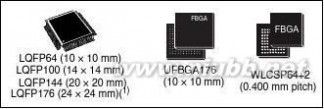
Table 1.
Reference
STM32F205xx
STM32F207xx
November 2010Doc ID 15818 Rev 51/147
www.st.com
This is preliminary information on a new product now in development or undergoing evaluation. Details are subject to change without notice.
205 STM32F205xx207xx参考手册
ContentsSTM32F205xx, STM32F207xxContents
1
2Introduction . . . . . . . . . . . . . . . . . . . . . . . . . . . . . . . . . . . . . . . . . . . . . . . . 9Description . . . . . . . . . . . . . . . . . . . . . . . . . . . . . . . . . . . . . . . . . . . . . . . . 10
2.1
2.2Full compatibility throughout the family . . . . . . . . . . . . . . . . . . . . . . . . . . 13Device overview . . . . . . . . . . . . . . . . . . . . . . . . . . . . . . . . . . . . . . . . . . . . 15
2.2.1
2.2.2
2.2.3
2.2.4
2.2.5
2.2.6
2.2.7
2.2.8
2.2.9
2.2.10
2.2.11
2.2.12
2.2.13
2.2.14
2.2.15
2.2.16
2.2.17
2.2.18
2.2.19
2.2.20
2.2.21
2.2.22
2.2.23
2.2.24
2.2.25
2.2.26
2.2.27
2.2.28ARM? Cortex?-M3 core with embedded Flash and SRAM . . . . . . . . . 16Memory protection unit . . . . . . . . . . . . . . . . . . . . . . . . . . . . . . . . . . . . . 16Adaptive real-time memory accelerator (ART Accelerator?) . . . . . . . . 16Embedded Flash memory . . . . . . . . . . . . . . . . . . . . . . . . . . . . . . . . . . . 16CRC (cyclic redundancy check) calculation unit . . . . . . . . . . . . . . . . . . 17True random number generator (RNG) . . . . . . . . . . . . . . . . . . . . . . . . . 17Embedded SRAM . . . . . . . . . . . . . . . . . . . . . . . . . . . . . . . . . . . . . . . . . 17Multi-AHB bus matrix . . . . . . . . . . . . . . . . . . . . . . . . . . . . . . . . . . . . . . . 17DMA . . . . . . . . . . . . . . . . . . . . . . . . . . . . . . . . . . . . . . . . . . . . . . . . . . . . 18FSMC (flexible static memory controller) . . . . . . . . . . . . . . . . . . . . . . . . 18Nested vectored interrupt controller (NVIC) . . . . . . . . . . . . . . . . . . . . . . 19External interrupt/event controller (EXTI) . . . . . . . . . . . . . . . . . . . . . . . 19Clocks and startup . . . . . . . . . . . . . . . . . . . . . . . . . . . . . . . . . . . . . . . . . 19Boot modes . . . . . . . . . . . . . . . . . . . . . . . . . . . . . . . . . . . . . . . . . . . . . . 20Power supply schemes . . . . . . . . . . . . . . . . . . . . . . . . . . . . . . . . . . . . . 20Power supply supervisor . . . . . . . . . . . . . . . . . . . . . . . . . . . . . . . . . . . . 20Voltage regulator . . . . . . . . . . . . . . . . . . . . . . . . . . . . . . . . . . . . . . . . . . 20Real-time clock (RTC), backup SRAM and backup registers . . . . . . . . 23Low-power modes . . . . . . . . . . . . . . . . . . . . . . . . . . . . . . . . . . . . . . . . . 23VBAT operation . . . . . . . . . . . . . . . . . . . . . . . . . . . . . . . . . . . . . . . . . . . . 24Timers and watchdogs . . . . . . . . . . . . . . . . . . . . . . . . . . . . . . . . . . . . . . 24Basic timers TIM6 and TIM7 . . . . . . . . . . . . . . . . . . . . . . . . . . . . . . . . . 26Independent watchdog . . . . . . . . . . . . . . . . . . . . . . . . . . . . . . . . . . . . . 26Window watchdog . . . . . . . . . . . . . . . . . . . . . . . . . . . . . . . . . . . . . . . . . 26SysTick timer . . . . . . . . . . . . . . . . . . . . . . . . . . . . . . . . . . . . . . . . . . . . . 27I2C bus . . . . . . . . . . . . . . . . . . . . . . . . . . . . . . . . . . . . . . . . . . . . . . . . . . 27Universal synchronous/asynchronous receiver transmitters(UARTs/USARTs) . . . . . . . . . . . . . . . . . . . . . . . . . . . . . . . . . . . . . . . . . 27Serial peripheral interface (SPI) . . . . . . . . . . . . . . . . . . . . . . . . . . . . . . . 28
扩展:stm32f207参考手册 / stm32f205参考手册 / stm32f207编程参考
2/147Doc ID 15818 Rev 5
205 STM32F205xx207xx参考手册
STM32F205xx, STM32F207xx2.2.29
2.2.30
2.2.31
2.2.32
2.2.33
2.2.34
2.2.35
2.2.36
2.2.37
2.2.38
2.2.39
2.2.40
2.2.41
2.2.42ContentsInter-integrated sound (I2S) . . . . . . . . . . . . . . . . . . . . . . . . . . . . . . . . . . 28SDIO . . . . . . . . . . . . . . . . . . . . . . . . . . . . . . . . . . . . . . . . . . . . . . . . . . . 28Ethernet MAC interface with dedicated DMA and IEEE1588 support . 29Controller area network (CAN) . . . . . . . . . . . . . . . . . . . . . . . . . . . . . . . 29Universal serial bus on-the-go full-speed (OTG_FS) . . . . . . . . . . . . . . . 29Universal serial bus on-the-go high-speed (OTG_HS) . . . . . . . . . . . . . 30Audio PLL (PLLI2S) . . . . . . . . . . . . . . . . . . . . . . . . . . . . . . . . . . . . . . . . 30Digital camera interface (DCMI) . . . . . . . . . . . . . . . . . . . . . . . . . . . . . . . 31GPIOs (general-purpose inputs/outputs) . . . . . . . . . . . . . . . . . . . . . . . . 31ADCs (analog-to-digital converters) . . . . . . . . . . . . . . . . . . . . . . . . . . . . 31DAC (digital-to-analog converter) . . . . . . . . . . . . . . . . . . . . . . . . . . . . . . 32Temperature sensor . . . . . . . . . . . . . . . . . . . . . . . . . . . . . . . . . . . . . . . . 32Serial wire JTAG debug port (SWJ-DP) . . . . . . . . . . . . . . . . . . . . . . . . . 32Embedded Trace Macrocell? . . . . . . . . . . . . . . . . . . . . . . . . . . . . . . . . 32
3
4
5Pinouts and pin description . . . . . . . . . . . . . . . . . . . . . . . . . . . . . . . . . . 33Memory mapping . . . . . . . . . . . . . . . . . . . . . . . . . . . . . . . . . . . . . . . . . . 53Electrical characteristics . . . . . . . . . . . . . . . . . . . . . . . . . . . . . . . . . . . . 54
5.1Parameter conditions . . . . . . . . . . . . . . . . . . . . . . . . . . . . . . . . . . . . . . . . 54
5.1.1
5.1.2
5.1.3
5.1.4
5.1.5
5.1.6
5.1.7Minimum and maximum values . . . . . . . . . . . . . . . . . . . . . . . . . . . . . . . 54Typical values . . . . . . . . . . . . . . . . . . . . . . . . . . . . . . . . . . . . . . . . . . . . . 54Typical curves . . . . . . . . . . . . . . . . . . . . . . . . . . . . . . . . . . . . . . . . . . . . 54Loading capacitor . . . . . . . . . . . . . . . . . . . . . . . . . . . . . . . . . . . . . . . . . 54Pin input voltage . . . . . . . . . . . . . . . . . . . . . . . . . . . . . . . . . . . . . . . . . . 54Power supply scheme . . . . . . . . . . . . . . . . . . . . . . . . . . . . . . . . . . . . . . 55Current consumption measurement . . . . . . . . . . . . . . . . . . . . . . . . . . . 55
5.2
5.3Absolute maximum ratings . . . . . . . . . . . . . . . . . . . . . . . . . . . . . . . . . . . . 56Operating conditions . . . . . . . . . . . . . . . . . . . . . . . . . . . . . . . . . . . . . . . . 57
5.3.1
5.3.2
5.3.3
5.3.4
5.3.5
5.3.6General operating conditions . . . . . . . . . . . . . . . . . . . . . . . . . . . . . . . . . 57Operating conditions at power-up / power-down (regulator not bypassed) . . . . . . . . . . . . . . . . . . . . . . . . . . . . . . . . . . . . 59Operating conditions at power-up / power-down in regulatorbypass mode . . . . . . . . . . . . . . . . . . . . . . . . . . . . . . . . . . . . . . . . . . . . . 60Embedded reset and power control block characteristics . . . . . . . . . . . 60Supply current characteristics . . . . . . . . . . . . . . . . . . . . . . . . . . . . . . . . 61External clock source characteristics . . . . . . . . . . . . . . . . . . . . . . . . . . . 67
Doc ID 15818 Rev 53/147
205 STM32F205xx207xx参考手册
Contents5.3.7
5.3.8
5.3.9
5.3.10
5.3.11
5.3.12
5.3.13
5.3.14
5.3.15
5.3.16
5.3.17
5.3.18
5.3.19
5.3.20
5.3.21
5.3.22
5.3.23
5.3.24
5.3.25
5.3.26STM32F205xx, STM32F207xxInternal clock source characteristics . . . . . . . . . . . . . . . . . . . . . . . . . . . 71Wakeup time from low-power mode . . . . . . . . . . . . . . . . . . . . . . . . . . . . 71PLL characteristics . . . . . . . . . . . . . . . . . . . . . . . . . . . . . . . . . . . . . . . . 72PLL spread spectrum clock generation (SSCG) characteristics . . . . . . 73Memory characteristics . . . . . . . . . . . . . . . . . . . . . . . . . . . . . . . . . . . . . 75EMC characteristics . . . . . . . . . . . . . . . . . . . . . . . . . . . . . . . . . . . . . . . . 76Absolute maximum ratings (electrical sensitivity) . . . . . . . . . . . . . . . . . 77I/O port characteristics . . . . . . . . . . . . . . . . . . . . . . . . . . . . . . . . . . . . . . 78NRST pin characteristics . . . . . . . . . . . . . . . . . . . . . . . . . . . . . . . . . . . . 82TIM timer characteristics . . . . . . . . . . . . . . . . . . . . . . . . . . . . . . . . . . . . 83Communications interfaces . . . . . . . . . . . . . . . . . . . . . . . . . . . . . . . . . . 8512-bit ADC characteristics . . . . . . . . . . . . . . . . . . . . . . . . . . . . . . . . . . . 98DAC electrical specifications . . . . . . . . . . . . . . . . . . . . . . . . . . . . . . . . 102Temperature sensor characteristics . . . . . . . . . . . . . . . . . . . . . . . . . . . 104VBAT monitoring characteristics . . . . . . . . . . . . . . . . . . . . . . . . . . . . . . 104Embedded reference voltage . . . . . . . . . . . . . . . . . . . . . . . . . . . . . . . . 104FSMC characteristics . . . . . . . . . . . . . . . . . . . . . . . . . . . . . . . . . . . . . . 105Camera interface (DCMI) timing specifications . . . . . . . . . . . . . . . . . . 123SD/SDIO MMC card host interface (SDIO) characteristics . . . . . . . . . 124RTC characteristics . . . . . . . . . . . . . . . . . . . . . . . . . . . . . . . . . . . . . . . 125
扩展:stm32f207参考手册 / stm32f205参考手册 / stm32f207编程参考
6Package characteristics . . . . . . . . . . . . . . . . . . . . . . . . . . . . . . . . . . . . 126
6.1
6.2Package mechanical data . . . . . . . . . . . . . . . . . . . . . . . . . . . . . . . . . . . 126Thermal characteristics . . . . . . . . . . . . . . . . . . . . . . . . . . . . . . . . . . . . . 133
7Part numbering . . . . . . . . . . . . . . . . . . . . . . . . . . . . . . . . . . . . . . . . . . . 134Appendix AApplication block diagrams . . . . . . . . . . . . . . . . . . . . . . . . . . . . . . 135
A.1
A.2
A.3
A.4
A.5Main applications versus package . . . . . . . . . . . . . . . . . . . . . . . . . . . . . 135Application example with regulator off. . . . . . . . . . . . . . . . . . . . . . . . . . . 136USB OTG full speed (FS) interface solutions . . . . . . . . . . . . . . . . . . . . . 137USB OTG high speed (HS) interface solutions. . . . . . . . . . . . . . . . . . . . 138Complete audio player solutions. . . . . . . . . . . . . . . . . . . . . . . . . . . . . . . 140
Revision history . . . . . . . . . . . . . . . . . . . . . . . . . . . . . . . . . . . . . . . . . . . . . . . . . . . 1434/147Doc ID 15818 Rev 5
205 STM32F205xx207xx参考手册
STM32F205xx, STM32F207xxList of tablesList of tables
Table 1.
Table 2.
Table 3.
Table 4.
Table 5.
Table 6.
Table 7.
Table 8.
Table 9.
Table 10.
Table 11.
Table 12.
Table 13.
Table 14.
Table 15.
Table 16.
Table 17.
Table 18.
Table 19.
Table 20.
Table 21.
Table 22.
Table 23.
Table 24.
Table 25.
Table 26.
Table 27.
Table 28.
Table 29.
Table 30.
Table 31.
Table 32.
Table 33.
Table 34.
Table 35.
Table 36.
Table 37.
Table 38.
Table 39.
Table 40.
Table 41.
Table 42.
Table 43.
Table 44.
Table 45.Device summary. . . . . . . . . . . . . . . . . . . . . . . . . . . . . . . . . . . . . . . . . . . . . . . . . . . . . . . . . . 1STM32F205xx and STM32F207xx features and peripheral counts . . . . . . . . . . . . . . . . . . 11Timer feature comparison. . . . . . . . . . . . . . . . . . . . . . . . . . . . . . . . . . . . . . . . . . . . . . . . . . 24USART feature comparison . . . . . . . . . . . . . . . . . . . . . . . . . . . . . . . . . . . . . . . . . . . . . . . . 27STM32F20x pin and ball definitions . . . . . . . . . . . . . . . . . . . . . . . . . . . . . . . . . . . . . . . . . . 38Alternate function mapping. . . . . . . . . . . . . . . . . . . . . . . . . . . . . . . . . . . . . . . . . . . . . . . . . 48Voltage characteristics . . . . . . . . . . . . . . . . . . . . . . . . . . . . . . . . . . . . . . . . . . . . . . . . . . . . 56Current characteristics . . . . . . . . . . . . . . . . . . . . . . . . . . . . . . . . . . . . . . . . . . . . . . . . . . . . 56Thermal characteristics. . . . . . . . . . . . . . . . . . . . . . . . . . . . . . . . . . . . . . . . . . . . . . . . . . . . 57General operating conditions . . . . . . . . . . . . . . . . . . . . . . . . . . . . . . . . . . . . . . . . . . . . . . . 57Limitations depending on the operating power supply range. . . . . . . . . . . . . . . . . . . . . . . 58Operating conditions at power-up / power-down (regulator not bypassed) . . . . . . . . . . . . 59Operating conditions at power-up / power-down in regulator bypass mode . . . . . . . . . . . . . . . . . . . . . . . . . . . . . . . . . . . . . . . . . . . . . . . . . . . . . . . . . . . 60Embedded reset and power control block characteristics. . . . . . . . . . . . . . . . . . . . . . . . . . 60Typical and maximum current consumption in Run mode, code with data processingrunning from Flash . . . . . . . . . . . . . . . . . . . . . . . . . . . . . . . . . . . . . . . . . . . . . . . . . . . . . . . 62Typical and maximum current consumption in Run mode, code with data processing running from RAM . . . . . . . . . . . . . . . . . . . . . . . . . . . . . . . . . . . . . . . . . . . . . . . . . . . . . . . 63Typical and maximum current consumption in Sleep mode. . . . . . . . . . . . . . . . . . . . . . . . 63Typical and maximum current consumptions in Stop mode. . . . . . . . . . . . . . . . . . . . . . . . 64Typical and maximum current consumptions in Standby mode . . . . . . . . . . . . . . . . . . . . . 64Typical and maximum current consumptions in VBAT mode. . . . . . . . . . . . . . . . . . . . . . . 65Peripheral current consumption . . . . . . . . . . . . . . . . . . . . . . . . . . . . . . . . . . . . . . . . . . . . . 65High-speed external user clock characteristics. . . . . . . . . . . . . . . . . . . . . . . . . . . . . . . . . . 67Low-speed external user clock characteristics. . . . . . . . . . . . . . . . . . . . . . . . . . . . . . . . . . 67HSE 4-26 MHz oscillator characteristics . . . . . . . . . . . . . . . . . . . . . . . . . . . . . . . . . . . . . . 69LSE oscillator characteristics (fLSE = 32.768 kHz) . . . . . . . . . . . . . . . . . . . . . . . . . . . . . . . 70HSI oscillator characteristics . . . . . . . . . . . . . . . . . . . . . . . . . . . . . . . . . . . . . . . . . . . . . . . 71LSI oscillator characteristics . . . . . . . . . . . . . . . . . . . . . . . . . . . . . . . . . . . . . . . . . . . . . . . 71Low-power mode wakeup timings . . . . . . . . . . . . . . . . . . . . . . . . . . . . . . . . . . . . . . . . . . . 72Main PLL characteristics. . . . . . . . . . . . . . . . . . . . . . . . . . . . . . . . . . . . . . . . . . . . . . . . . . . 72PLLI2S (audio PLL) characteristics . . . . . . . . . . . . . . . . . . . . . . . . . . . . . . . . . . . . . . . . . . 72SSCG parameters constraint . . . . . . . . . . . . . . . . . . . . . . . . . . . . . . . . . . . . . . . . . . . . . . . 73Flash memory characteristics. . . . . . . . . . . . . . . . . . . . . . . . . . . . . . . . . . . . . . . . . . . . . . . 75Flash memory programming. . . . . . . . . . . . . . . . . . . . . . . . . . . . . . . . . . . . . . . . . . . . . . . . 75Flash memory programming with VPP . . . . . . . . . . . . . . . . . . . . . . . . . . . . . . . . . . . . . . . . . . . . . . . . . . .75Flash memory endurance and data retention. . . . . . . . . . . . . . . . . . . . . . . . . . . . . . . . . . . 76EMS characteristics . . . . . . . . . . . . . . . . . . . . . . . . . . . . . . . . . . . . . . . . . . . . . . . . . . . . . . 76EMI characteristics. . . . . . . . . . . . . . . . . . . . . . . . . . . . . . . . . . . . . . . . . . . . . . . . . . . . . . . 77ESD absolute maximum ratings. . . . . . . . . . . . . . . . . . . . . . . . . . . . . . . . . . . . . . . . . . . . . 78Electrical sensitivities . . . . . . . . . . . . . . . . . . . . . . . . . . . . . . . . . . . . . . . . . . . . . . . . . . . . . 78I/O static characteristics . . . . . . . . . . . . . . . . . . . . . . . . . . . . . . . . . . . . . . . . . . . . . . . . . . . 78Output voltage characteristics . . . . . . . . . . . . . . . . . . . . . . . . . . . . . . . . . . . . . . . . . . . . . . 80I/O AC characteristics. . . . . . . . . . . . . . . . . . . . . . . . . . . . . . . . . . . . . . . . . . . . . . . . . . . . . 80NRST pin characteristics . . . . . . . . . . . . . . . . . . . . . . . . . . . . . . . . . . . . . . . . . . . . . . . . . . 82Characteristics of TIMx connected to the APB1 domain . . . . . . . . . . . . . . . . . . . . . . . . . . 83Characteristics of TIMx connected to the APB2 domain . . . . . . . . . . . . . . . . . . . . . . . . . . 84
扩展:stm32f207参考手册 / stm32f205参考手册 / stm32f207编程参考
Doc ID 15818 Rev 55/147
205 STM32F205xx207xx参考手册
List of tablesTable 46.
Table 47.
Table 48.
Table 49.
Table 50.
Table 51.
Table 52.
Table 53.
Table 54.
Table 55.
Table 56.
Table 57.
Table 58.
Table 59.
Table 60.
Table 61.
Table 62.
Table 63.
Table 64.
Table 65.
Table 66.
Table 67.
Table 68.
Table 69.
Table 70.
Table 71.
Table 72.
Table 73.
Table 74.
Table 75.
Table 76.
Table 77.
Table 78.
Table 79.
Table 80.
Table 81.
Table 82.
Table 83.
Table 84.
Table 85.
Table 86.
Table 87.STM32F205xx, STM32F207xxI2C characteristics. . . . . . . . . . . . . . . . . . . . . . . . . . . . . . . . . . . . . . . . . . . . . . . . . . . . . . . . 85SCL frequency (fPCLK1= 30 MHz.,VDD = 3.3 V) . . . . . . . . . . . . . . . . . . . . . . . . . . . . . . . . . 86SPI characteristics . . . . . . . . . . . . . . . . . . . . . . . . . . . . . . . . . . . . . . . . . . . . . . . . . . . . . . . 87I2S characteristics . . . . . . . . . . . . . . . . . . . . . . . . . . . . . . . . . . . . . . . . . . . . . . . . . . . . . . . 90USB OTG FS startup time . . . . . . . . . . . . . . . . . . . . . . . . . . . . . . . . . . . . . . . . . . . . . . . . . 92USB OTG FS DC electrical characteristics. . . . . . . . . . . . . . . . . . . . . . . . . . . . . . . . . . . . . 92USB OTG FS electrical characteristics. . . . . . . . . . . . . . . . . . . . . . . . . . . . . . . . . . . . . . . . 94Clock timing parameters. . . . . . . . . . . . . . . . . . . . . . . . . . . . . . . . . . . . . . . . . . . . . . . . . . . 94ULPI timing. . . . . . . . . . . . . . . . . . . . . . . . . . . . . . . . . . . . . . . . . . . . . . . . . . . . . . . . . . . . . 95Ethernet DC electrical characteristics. . . . . . . . . . . . . . . . . . . . . . . . . . . . . . . . . . . . . . . . . 95Dynamics characteristics: Ethernet MAC signals for SMI. . . . . . . . . . . . . . . . . . . . . . . . . . 96Dynamics characteristics: Ethernet MAC signals for RMII . . . . . . . . . . . . . . . . . . . . . . . . . 96Dynamics characteristics: Ethernet MAC signals for MII . . . . . . . . . . . . . . . . . . . . . . . . . . 97ADC characteristics . . . . . . . . . . . . . . . . . . . . . . . . . . . . . . . . . . . . . . . . . . . . . . . . . . . . . . 98ADC accuracy . . . . . . . . . . . . . . . . . . . . . . . . . . . . . . . . . . . . . . . . . . . . . . . . . . . . . . . . . . 99DAC characteristics . . . . . . . . . . . . . . . . . . . . . . . . . . . . . . . . . . . . . . . . . . . . . . . . . . . . . 102TS characteristics. . . . . . . . . . . . . . . . . . . . . . . . . . . . . . . . . . . . . . . . . . . . . . . . . . . . . . . 104VBAT monitoring characteristics . . . . . . . . . . . . . . . . . . . . . . . . . . . . . . . . . . . . . . . . . . . . 104Embedded internal reference voltage. . . . . . . . . . . . . . . . . . . . . . . . . . . . . . . . . . . . . . . . 104Asynchronous non-multiplexed SRAM/PSRAM/NOR read timings . . . . . . . . . . . . . . . . . 106Asynchronous non-multiplexed SRAM/PSRAM/NOR write timings . . . . . . . . . . . . . . . . . 107Asynchronous multiplexed PSRAM/NOR read timings. . . . . . . . . . . . . . . . . . . . . . . . . . . 108Asynchronous multiplexed PSRAM/NOR write timings . . . . . . . . . . . . . . . . . . . . . . . . . . 109Synchronous multiplexed NOR/PSRAM read timings . . . . . . . . . . . . . . . . . . . . . . . . . . . 111Synchronous multiplexed PSRAM write timings. . . . . . . . . . . . . . . . . . . . . . . . . . . . . . . . 113Synchronous non-multiplexed NOR/PSRAM read timings. . . . . . . . . . . . . . . . . . . . . . . . 114Synchronous non-multiplexed PSRAM write timings . . . . . . . . . . . . . . . . . . . . . . . . . . . . 115Switching characteristics for PC Card/CF read and write cycles . . . . . . . . . . . . . . . . . . . 120Switching characteristics for NAND Flash read and write cycles . . . . . . . . . . . . . . . . . . . 123DCMI characteristics. . . . . . . . . . . . . . . . . . . . . . . . . . . . . . . . . . . . . . . . . . . . . . . . . . . . . 123SD / MMC characteristics. . . . . . . . . . . . . . . . . . . . . . . . . . . . . . . . . . . . . . . . . . . . . . . . . 124RTC characteristics . . . . . . . . . . . . . . . . . . . . . . . . . . . . . . . . . . . . . . . . . . . . . . . . . . . . . 125LQFP64 – 10 x 10 mm 64 pin low-profile quad flat package mechanical data. . . . . . . . . 127WLCSP64+2 - 0.400 mm pitch wafer level chip size package mechanical data . . . . . . . 128LQPF100 – 14 x 14 mm 100-pin low-profile quad flat package mechanical data. . . . . . . 129LQFP144, 20 x 20 mm, 144-pin low-profile quad flat package mechanical data . . . . . . . 130LQFP176 - Low profile quad flat package 24 × 24 × 1.4 mm package mechanical data . 131UFBGA176+25 - ultra thin fine pitch ball grid array 10 × 10 × 0.6 mm mechanical data . 132Package thermal characteristics. . . . . . . . . . . . . . . . . . . . . . . . . . . . . . . . . . . . . . . . . . . . 133Ordering information scheme. . . . . . . . . . . . . . . . . . . . . . . . . . . . . . . . . . . . . . . . . . . . . . 134Main applications versus package for STM32F207xx microcontrollers . . . . . . . . . . . . . . 135Document revision history . . . . . . . . . . . . . . . . . . . . . . . . . . . . . . . . . . . . . . . . . . . . . . . . 1436/147Doc ID 15818 Rev 5
扩展:stm32f207参考手册 / stm32f205参考手册 / stm32f207编程参考
205 STM32F205xx207xx参考手册
STM32F205xx, STM32F207xxList of figuresList of figures
Figure 1.
Figure 2.
Figure 3.
Figure 4.
Figure 5.
Figure 6.
Figure 7.
Figure 8.
Figure 9.
Figure 10.
Figure 11.
Figure 12.
Figure 13.
Figure 14.
Figure 15.
Figure 16.
Figure 17.
Figure 18.
Figure 19.
Figure 20.
Figure 21.
Figure 22.
Figure 23.
Figure 24.
Figure 25.
Figure 26.
Figure 27.
Figure 28.
Figure 29.
Figure 30.
Figure 31.
Figure 32.
Figure 33.
Figure 34.
Figure 35.
Figure 36.
Figure 37.
Figure 38.
Figure 39.
Figure 40.
Figure 41.
Figure 42.
Figure 43.
Figure 44.
Figure 45.
Figure 46.Compatible board design: LQFP144 . . . . . . . . . . . . . . . . . . . . . . . . . . . . . . . . . . . . . . . . . 13Compatible board design: LQFP100 . . . . . . . . . . . . . . . . . . . . . . . . . . . . . . . . . . . . . . . . . 14Compatible board design: LQFP64 . . . . . . . . . . . . . . . . . . . . . . . . . . . . . . . . . . . . . . . . . . 14STM32F20x block diagram. . . . . . . . . . . . . . . . . . . . . . . . . . . . . . . . . . . . . . . . . . . . . . . . . 15Multi-AHB matrix. . . . . . . . . . . . . . . . . . . . . . . . . . . . . . . . . . . . . . . . . . . . . . . . . . . . . . . . . 17Startup in regulator bypass/regulator off mode: slow VDD slope - power-down reset risen after VCAP_1/VCAP_2 stabilization. . . . . . . . . . . . . . . . . . . . . . . . 22Startup in regulator bypass/regulator off mode: slow VDD slope - power-down reset risen before VCAP_1/VCAP_2 stabilization . . . . . . . . . . . . . . . . . . . . . . 22Sartup in regulator bypass/regulator off and internal reset off . . . . . . . . . . . . . . . . . . . . . . 22STM32F20x LQFP64 pinout. . . . . . . . . . . . . . . . . . . . . . . . . . . . . . . . . . . . . . . . . . . . . . . . 33STM32F20x WLCSP64+2 ballout. . . . . . . . . . . . . . . . . . . . . . . . . . . . . . . . . . . . . . . . . . . . 33STM32F20x LQFP100 pinout. . . . . . . . . . . . . . . . . . . . . . . . . . . . . . . . . . . . . . . . . . . . . . . 34STM32F20x LQFP144 pinout. . . . . . . . . . . . . . . . . . . . . . . . . . . . . . . . . . . . . . . . . . . . . . . 35STM32F20x LQFP176 pinout. . . . . . . . . . . . . . . . . . . . . . . . . . . . . . . . . . . . . . . . . . . . . . . 36STM32F21xxx UFBGA176 ballout . . . . . . . . . . . . . . . . . . . . . . . . . . . . . . . . . . . . . . . . . . . 37Memory map. . . . . . . . . . . . . . . . . . . . . . . . . . . . . . . . . . . . . . . . . . . . . . . . . . . . . . . . . . . . 53Pin loading conditions. . . . . . . . . . . . . . . . . . . . . . . . . . . . . . . . . . . . . . . . . . . . . . . . . . . . . 54Pin input voltage. . . . . . . . . . . . . . . . . . . . . . . . . . . . . . . . . . . . . . . . . . . . . . . . . . . . . . . . . 54Power supply scheme. . . . . . . . . . . . . . . . . . . . . . . . . . . . . . . . . . . . . . . . . . . . . . . . . . . . . 55Current consumption measurement scheme . . . . . . . . . . . . . . . . . . . . . . . . . . . . . . . . . . . 55Number of wait states versus fCPU and VDD range. . . . . . . . . . . . . . . . . . . . . . . . . . . . . . . 59High-speed external clock source AC timing diagram . . . . . . . . . . . . . . . . . . . . . . . . . . . . 68Low-speed external clock source AC timing diagram. . . . . . . . . . . . . . . . . . . . . . . . . . . . . 68Typical application with an 8 MHz crystal. . . . . . . . . . . . . . . . . . . . . . . . . . . . . . . . . . . . . . 69Typical application with a 32.768 kHz crystal. . . . . . . . . . . . . . . . . . . . . . . . . . . . . . . . . . . 70PLL output clock waveforms in center spread mode . . . . . . . . . . . . . . . . . . . . . . . . . . . . . 74PLL output clock waveforms in down spread mode. . . . . . . . . . . . . . . . . . . . . . . . . . . . . . 74I/O AC characteristics definition . . . . . . . . . . . . . . . . . . . . . . . . . . . . . . . . . . . . . . . . . . . . . 82Recommended NRST pin protection . . . . . . . . . . . . . . . . . . . . . . . . . . . . . . . . . . . . . . . . . 83I2C bus AC waveforms and measurement circuit. . . . . . . . . . . . . . . . . . . . . . . . . . . . . . . . 86SPI timing diagram - slave mode and CPHA = 0 . . . . . . . . . . . . . . . . . . . . . . . . . . . . . . . . 88SPI timing diagram - slave mode and CPHA = 1(1) . . . . . . . . . . . . . . . . . . . . . . . . . . . . . . 88SPI timing diagram - master mode(1) . . . . . . . . . . . . . . . . . . . . . . . . . . . . . . . . . . . . . . . . . 89I2S slave timing diagram (Philips protocol)(1) . . . . . . . . . . . . . . . . . . . . . . . . . . . . . . . . . . . 91I2S master timing diagram (Philips protocol)(1). . . . . . . . . . . . . . . . . . . . . . . . . . . . . . . . . . 91USB OTG FS timings: definition of data signal rise and fall time . . . . . . . . . . . . . . . . . . . . 93ULPI timing diagram. . . . . . . . . . . . . . . . . . . . . . . . . . . . . . . . . . . . . . . . . . . . . . . . . . . . . . 95Ethernet SMI timing diagram . . . . . . . . . . . . . . . . . . . . . . . . . . . . . . . . . . . . . . . . . . . . . . . 96Ethernet RMII timing diagram. . . . . . . . . . . . . . . . . . . . . . . . . . . . . . . . . . . . . . . . . . . . . . . 96Ethernet MII timing diagram . . . . . . . . . . . . . . . . . . . . . . . . . . . . . . . . . . . . . . . . . . . . . . . . 97ADC accuracy characteristics. . . . . . . . . . . . . . . . . . . . . . . . . . . . . . . . . . . . . . . . . . . . . . 100Typical connection diagram using the ADC . . . . . . . . . . . . . . . . . . . . . . . . . . . . . . . . . . . 100Power supply and reference decoupling (VREF+ not connected to VDDA). . . . . . . . . . . . . 101Power supply and reference decoupling (VREF+ connected to VDDA). . . . . . . . . . . . . . . . 10112-bit buffered /non-buffered DAC . . . . . . . . . . . . . . . . . . . . . . . . . . . . . . . . . . . . . . . . . . 103Asynchronous non-multiplexed SRAM/PSRAM/NOR read waveforms . . . . . . . . . . . . . . 105Asynchronous non-multiplexed SRAM/PSRAM/NOR write waveforms . . . . . . . . . . . . . . 106
扩展:stm32f207参考手册 / stm32f205参考手册 / stm32f207编程参考
Doc ID 15818 Rev 57/147
205 STM32F205xx207xx参考手册
List of figuresFigure 47.
Figure 48.
Figure 49.
Figure 50.
Figure 51.
Figure 52.
Figure 53.
Figure 54.
Figure 55.
Figure 56.
Figure 57.
Figure 58.
Figure 59.
Figure 60.
Figure 61.
Figure 62.
Figure 63.
Figure 64.
Figure 65.
Figure 66.
Figure 67.
Figure 68.
Figure 69.
Figure 70.
Figure 71.
Figure 72.
Figure 73.
Figure 74.
Figure 75.
Figure 76.
Figure 77.
Figure 78.
Figure 79.
Figure 80.
Figure 81.
Figure 82.
Figure 83.
Figure 84.
Figure 85.
Figure 86.
Figure 87.STM32F205xx, STM32F207xxAsynchronous multiplexed PSRAM/NOR read waveforms. . . . . . . . . . . . . . . . . . . . . . . . 107Asynchronous multiplexed PSRAM/NOR write waveforms . . . . . . . . . . . . . . . . . . . . . . . 109Synchronous multiplexed NOR/PSRAM read timings . . . . . . . . . . . . . . . . . . . . . . . . . . . 110Synchronous multiplexed PSRAM write timings. . . . . . . . . . . . . . . . . . . . . . . . . . . . . . . . 112Synchronous non-multiplexed NOR/PSRAM read timings. . . . . . . . . . . . . . . . . . . . . . . . 114Synchronous non-multiplexed PSRAM write timings . . . . . . . . . . . . . . . . . . . . . . . . . . . . 115PC Card/CompactFlash controller waveforms for common memory read access. . . . . . 116PC Card/CompactFlash controller waveforms for common memory write access. . . . . . 117PC Card/CompactFlash controller waveforms for attribute memory readaccess. . . . . . . . . . . . . . . . . . . . . . . . . . . . . . . . . . . . . . . . . . . . . . . . . . . . . . . . . . . . . . . . 118PC Card/CompactFlash controller waveforms for attribute memory writeaccess. . . . . . . . . . . . . . . . . . . . . . . . . . . . . . . . . . . . . . . . . . . . . . . . . . . . . . . . . . . . . . . . 119PC Card/CompactFlash controller waveforms for I/O space read access . . . . . . . . . . . . 119PC Card/CompactFlash controller waveforms for I/O space write access. . . . . . . . . . . . 120NAND controller waveforms for read access . . . . . . . . . . . . . . . . . . . . . . . . . . . . . . . . . . 122NAND controller waveforms for write access . . . . . . . . . . . . . . . . . . . . . . . . . . . . . . . . . . 122NAND controller waveforms for common memory read access. . . . . . . . . . . . . . . . . . . . 122NAND controller waveforms for common memory write access. . . . . . . . . . . . . . . . . . . . 123SDIO high-speed mode . . . . . . . . . . . . . . . . . . . . . . . . . . . . . . . . . . . . . . . . . . . . . . . . . . 124SD default mode. . . . . . . . . . . . . . . . . . . . . . . . . . . . . . . . . . . . . . . . . . . . . . . . . . . . . . . . 124LQFP64 – 10 x 10 mm 64 pin low-profile quad flat package outline . . . . . . . . . . . . . . . . 127Recommended footprint(1) . . . . . . . . . . . . . . . . . . . . . . . . . . . . . . . . . . . . . . . . . . . . . . . . 127WLCSP64+2 - 0.400 mm pitch wafer level chip size package outline . . . . . . . . . . . . . . . 128LQFP100, 14 x 14 mm 100-pin low-profile quad flat package outline . . . . . . . . . . . . . . . 129Recommended footprint(1) . . . . . . . . . . . . . . . . . . . . . . . . . . . . . . . . . . . . . . . . . . . . . . . . 129LQFP144, 20 x 20 mm, 144-pin low-profile quadflat package outline. . . . . . . . . . . . . . . . . . . . . . . . . . . . . . . . . . . . . . . . . . . . . . . . . . . . . . 130Recommended footprint(1) . . . . . . . . . . . . . . . . . . . . . . . . . . . . . . . . . . . . . . . . . . . . . . . . 130LQFP176 - Low profile quad flat package 24 × 24 × 1.4 mm, package outline . . . . . . . . 131UFBGA176+25 - ultra thin fine pitch ball grid array 10 × 10 × 0.6 mm, package outline . 132Regulator bypass/regulator off . . . . . . . . . . . . . . . . . . . . . . . . . . . . . . . . . . . . . . . . . . . . . 136Regulator bypass/regulator off and internal reset off . . . . . . . . . . . . . . . . . . . . . . . . . . . . 136USB OTG FS peripheral-only connection. . . . . . . . . . . . . . . . . . . . . . . . . . . . . . . . . . . . . 137USB OTG FS host-only connection . . . . . . . . . . . . . . . . . . . . . . . . . . . . . . . . . . . . . . . . . 137OTG FS connection dual-role with internal PHY . . . . . . . . . . . . . . . . . . . . . . . . . . . . . . . 138USB OTG HS peripheral-only connection . . . . . . . . . . . . . . . . . . . . . . . . . . . . . . . . . . . . 138USB OTG HS host-only connection . . . . . . . . . . . . . . . . . . . . . . . . . . . . . . . . . . . . . . . . . 139OTG HS connection dual-role with external PHY. . . . . . . . . . . . . . . . . . . . . . . . . . . . . . . 139Complete audio player solution 1. . . . . . . . . . . . . . . . . . . . . . . . . . . . . . . . . . . . . . . . . . . 140Complete audio player solution 2. . . . . . . . . . . . . . . . . . . . . . . . . . . . . . . . . . . . . . . . . . . 140Audio player solution using PLL, PLLI2S, USB and 1 crystal. . . . . . . . . . . . . . . . . . . . . . 141Audio PLL (PLLI2S) providing accurate I2S clock . . . . . . . . . . . . . . . . . . . . . . . . . . . . . . 141Master clock (MCK) used to drive the external audio DAC. . . . . . . . . . . . . . . . . . . . . . . . 142Master clock (MCK) not used to drive the external audio DAC. . . . . . . . . . . . . . . . . . . . . 1428/147Doc ID 15818 Rev 5
扩展:stm32f207参考手册 / stm32f205参考手册 / stm32f207编程参考
205 STM32F205xx207xx参考手册
STM32F205xx, STM32F207xxIntroduction1 Introduction
This datasheet provides the description of the STM32F205xx and STM32F207xx lines of
microcontrollers. For more details on the whole STMicroelectronics STM32? family, please
refer to Section2.1: Full compatibility throughout the family.
The STM32F205xx and STM32F207xx datasheet should be read in conjunction with the
STM32F20x/STM32F21x reference manual.
For information on programming, erasing and protection of the internal Flash memory,
please refer to the STM32F20x/STM32F21x Flash programming manual.
The reference and Flash programming manuals are both available from the
STMicroelectronics website www.st.com.
For information on the Cortex?-M3 core please refer to the Cortex?-M3 Technical
Reference Manual, available from the www.arm.com website at the following address:
http://infocenter.arm.com/help/index.jsp?topic=/com.arm.doc.ddi0337e/.
Doc ID 15818 Rev 59/147
205 STM32F205xx207xx参考手册
DescriptionSTM32F205xx, STM32F207xx2 Description
The STM32F205xx and STM32F207xx family is based on the high-performance ARM?
Cortex?-M3 32-bit RISC core operating at a frequency of up to 120 MHz. The family
incorporates high-speed embedded memories (Flash memory up to 1 Mbyte, up to
128Kbytes of system SRAM), up to 4Kbytes of backup SRAM, and an extensive range of
enhanced I/Os and peripherals connected to two APB buses, two AHB buses and a 32-bit
multi-AHB bus matrix.
The devices also feature an adaptive real-time memory accelerator (ART Accelerator?)
which allows to achieve a performance equivalent to 0 wait state program execution from
Flash memory at a CPU frequency up to 120MHz. This performance has been validated
using the CoreMark benchmark.
All devices offer three 12-bit ADCs, two DACs, a low-power RTC, twelve general-purpose
16-bit timers including two PWM timers for motor control, two general-purpose 32-bit timers.
a true number random generator (RNG). They also feature standard and advanced
communication interfaces. New advanced peripherals include an SDIO, an enhanced
flexible static memory control (FSMC) interface (for devices offered in packages of 100 pins
and more), and a camera interface for CMOS sensors.
●
●Up to three I2CsThree SPIs, two I2Ss. To achieve audio class accuracy, the I2S peripherals can be
clocked via a dedicated internal audio PLL or via an external PLL to allow
synchronization.
4 USARTs and 2 UARTs
An USB OTG full-speed and a USB OTG full-speed with high-speed capability (with the ULPI),
Two CANs
An SDIO interface
Ethernet and the camera interface available on STM32F207xx devices only.●●●●●
The STM32F205xx and STM32F207xx family operates in the –40 to +105°C temperature
range from a 1.8V to 3.6V power supply. A comprehensive set of power-saving mode
allows the design of low-power applications.
The STM32F205xx and STM32F207xx family offers devices in four packages ranging from
64 pins to 176 pins. The set of included peripherals changes with the device chosen.
These features make the STM32F205xx and STM32F207xx microcontroller family suitable
for a wide range of applications:
●
●
●
●
●
●Motor drive and application controlMedical equipmentIndustrial applications: PLC, inverters, circuit breakersPrinters, and scannersAlarm systems, video intercom, and HVACHome audio appliances
Figure4 shows the general block diagram of the device family.
10/147Doc ID 15818 Rev 5
205 STM32F205xx207xx参考手册
Table 2.STM32F205xx and STM32F207xx features and peripheral counts
PeripheralsSTM32F205RxSTM32F205VxSTM32F205ZxSTM32F207VxSTM32F207ZxSTM32F207IxFlash memory in
Kbytes128256512768102412825651276810242565127681024256512768102425651276810242565127681024SRAM in System6496649696
Kbytes(48+16)(80+16)128(112+16)(48+16)(80+16)128 (112+16)(80+16)128 (112+16)128 (112+16)
Backup4444
FSMC memory
controllerNoYes
EthernetNoYes
General-
purpose10
TimersAdvanced
-control2
Doc ID 15818 Rev 5Basic2
Random number
generatorYes
SPI / (I2S)3 (2)
IC3
USART4
Comm. UART2
interfacesUSB OTG
FS
USB OTG 1HS/FS1FS, 1HS/FS
HS
CAN2
Camera interfaceNoYes
GPIOs51821148211414012-bit ADC3
Number of channels16162416242412-bit DACYes
Number of channels2
11/147STM32F205xx, STM32F207xxDescription
205 STM32F205xx207xx参考手册
12/147Table 2.STM32F205xx and STM32F207xx features and peripheral counts (continued)
PeripheralsSTM32F205RxSTM32F205VxSTM32F205ZxSTM32F207VxSTM32F207ZxSTM32F207IxMaximum CPU
扩展:stm32f207参考手册 / stm32f205参考手册 / stm32f207编程参考
frequency 120 MHz
Operating voltage 1.8 V to 3.6 V
Operating Ambient temperatures: –40 to +85 °C /–40 to +105 °C
temperaturesJunction temperature: –40 to + 125 °C
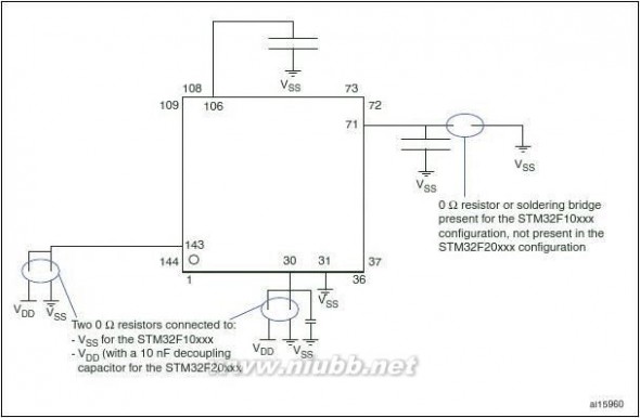
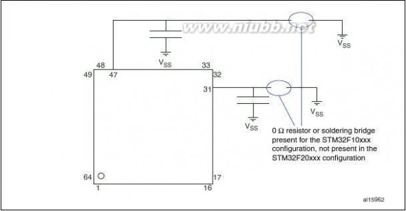
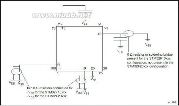
LQFP64PackageWLCSP64+2LQFP100LQFP144LQFP100LQFP144LQFP176
UFBGA176
1.Package not in production and available for development only.
Doc ID 15818 Rev 5DescriptionSTM32F205xx, STM32F207xx
205 STM32F205xx207xx参考手册
STM32F205xx, STM32F207xxDescription
2.1 Full compatibility throughout the family
The STM32F205xx and STM32F207xx constitute the STM32F20x family whose members
are fully pin-to-pin, software and feature compatible, allowing the user to try different
memory densities and peripherals for a greater degree of freedom during the development
cycle.
The STM32F205xx and STM32F207xx devices maintain a close compatibility with the
whole STM32F10xxx family. All functional pins are pin-to-pin compatible. The
STM32F205xx and STM32F207xx, however, are not drop-in replacements for the
STM32F10xxx devices: the two families do not have the same power scheme, and so their
power pins are different. Nonetheless, transition from the STM32F10xxx to the STM32F20x
family remains simple as only a few pins are impacted.
Figure1 compatible board design between the STM32F20x and the STM32F10xxx family.
Doc ID 15818 Rev 513/147
205 STM32F205xx207xx参考手册
Description
STM32F205xx, STM32F207xx14/147Doc ID 15818 Rev 5
205 STM32F205xx207xx参考手册
STM32F205xx, STM32F207xxDescription
2.2 Device overview

Doc ID 15818 Rev 515/147
205 STM32F205xx207xx参考手册
DescriptionSTM32F205xx, STM32F207xx2.2.1 ARM? Cortex?-M3 core with embedded Flash and SRAM
The ARM Cortex-M3 processor is the latest generation of ARM processors for embedded
systems. It was developed to provide a low-cost platform that meets the needs of MCU
implementation, with a reduced pin count and low-power consumption, while delivering
outstanding computational performance and an advanced response to interrupts.
The ARM Cortex-M3 32-bit RISC processor features exceptional code-efficiency, delivering
the high-performance expected from an ARM core in the memory size usually associated
with 8- and 16-bit devices.
With its embedded ARM core, the STM32F205xx and STM32F207xx family is compatible
with all ARM tools and software.
Figure 1 shows the general block diagram of the STM32F20x family.
2.2.2 Memory protection unit
The memory protection unit (MPU) is used to separate the processing of tasks from the data
protection. The MPU can manage up to 8 protection areas that can all be further divided up
into 8 subareas. The protection area sizes are between 32 bytes and the whole 4 gigabytes
of addressable memory.
The memory protection unit is especially helpful for applications where some critical or
certified code has to be protected against the misbehavior of other tasks. It is usually
managed by an RTOS (real-time operating system). If a program accesses a memory
location that is prohibited by the MPU, the RTOS can detect it and take action. In an RTOS
environment, the kernel can dynamically update the MPU area setting, based on the
process to be executed.
The MPU is optional and can be bypassed for applications that do not need it.
2.2.3 Adaptive real-time memory accelerator (ART Accelerator?)
The ART Accelerator? is a memory accelerator which is optimized for STM32 industry-
standard ARM? Cortex?-M3 processors. It balances the inherent performance advantage
of the ARM Cortex-M3 over Flash memory technologies, which normally requires the
processor to wait for the Flash memory at higher operating frequencies.
To release the processor full 150 DMIPS performance at this frequency, the accelerator
implements an instruction prefetch queue and branch cache which increases program
execution speed from the 128-bit Flash memory. Based on CoreMark benchmark, the
performance achieved thanks to the ART accelerator is equivalent to 0 wait state program
execution from Flash memory at a CPU frequency up to 120MHz.
2.2.4 Embedded Flash memory
The STM32F20x devices embed a 128-bit wide Flash memory of 128 Kbytes, 256 Kbytes,
512 Kbytes, 768 Kbytes or 1 Mbytes available for storing programs and data.
扩展:stm32f207参考手册 / stm32f205参考手册 / stm32f207编程参考
16/147Doc ID 15818 Rev 5
205 STM32F205xx207xx参考手册
STM32F205xx, STM32F207xxDescription
2.2.5 CRC (cyclic redundancy check) calculation unit
The CRC (cyclic redundancy check) calculation unit is used to get a CRC code from a 32-bit data word and a fixed generator polynomial.
Among other applications, CRC-based techniques are used to verify data transmission or storage integrity. In the scope of the EN/IEC 60335-1 standard, they offer a means of verifying the Flash memory integrity. The CRC calculation unit helps compute a software signature during runtime, to be compared with a reference signature generated at link-time and stored at a given memory location.
2.2.6 True random number generator (RNG)
All STM32F2xxx products embed a true RNG that delivers 32-bit random numbers
produced by an integrated analog circuit.
2.2.7 Embedded SRAM
All STM32F20x products embed up to 128 Kbytes of system SRAM accessed (read/write) at
CPU clock speed with 0 wait states, plus 4 Kbytes of backup SRAM.
2.2.8 Multi-AHB bus matrix
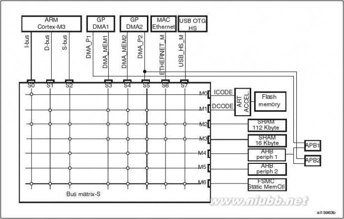
The 32-bit multi-AHB bus matrix interconnects all the masters (CPU, DMAs, Ethernet, USB HS) and the slaves (Flash memory, RAM, FSMC, AHB and APB peripherals) and ensures a seamless and efficient operation even when several high-speed peripherals work simultaneously.
Doc ID 15818 Rev 517/147
205 STM32F205xx207xx参考手册
DescriptionSTM32F205xx, STM32F207xx2.2.9 DMA
The flexible 16-stream general-purpose DMAs (8 streams for DMA1 and 8 streams for
DMA2) are able to manage memory-to-memory, peripheral-to-memory and memory-to-
peripheral transfers. They share some centralized FIFOs for APB/AHB peripherals, support
burst transfer and are designed to provide the maximum peripheral bandwidth (AHB/APB)
and performance.
The two DMA controllers support circular buffer management, so that no specific code is
needed when the controller reaches the end of the buffer. The two DMA controllers also
have a double buffering feature, which automates the use and switching of two memory
buffers without requiring any special code.
Each stream is connected to dedicated hardware DMA requests, with support for software
trigger on each stream. Configuration is made by software and transfer sizes between
source and destination are independent.
The DMA can be used with the main peripherals:
●
●
●
●
●
●
●
●SPI and I2SI2CUSART and UARTGeneral-purpose, basic and advanced-control timers TIMxDACSDIOCamera interface (DCMI)ADC.
2.2.10 FSMC (flexible static memory controller)
The FSMC is embedded in the STM32F205xx and STM32F207xx family. It has four Chip
Select outputs supporting the following modes: PCCard/Compact Flash, SRAM, PSRAM,
NOR Flash and NAND Flash.
Functionality overview:
●
●
●Write FIFOCode execution from external memory except for NAND Flash and PC CardThe targeted frequency, fCLK, is equal to HCLK/2, so external access is at 60 MHz
when HCLK is at 120 MHz and external access is at 30 MHz when HCLK is at 60 MHz
LCD parallel interface
The FSMC can be configured to interface seamlessly with most graphic LCD controllers. It
supports the Intel 8080 and Motorola 6800 modes, and is flexible enough to adapt to
specific LCD interfaces. This LCD parallel interface capability makes it easy to build cost-
effective graphic applications using LCD modules with embedded controllers or high
performance solutions using external controllers with dedicated acceleration.
18/147Doc ID 15818 Rev 5
205 STM32F205xx207xx参考手册
STM32F205xx, STM32F207xxDescription
2.2.11 Nested vectored interrupt controller (NVIC)
The STM32F205xx and STM32F207xx embed a nested vectored interrupt controller able to
handle up to 87 maskable interrupt channels (not including the 16 interrupt lines of the
Cortex?-M3) and 16 priority levels.
●
●
●
●
●
●
●
●Closely coupled NVIC gives low-latency interrupt processingInterrupt entry vector table address passed directly to the coreClosely coupled NVIC core interfaceAllows early processing of interruptsProcessing of late arriving, higher-priority interruptsSupport tail chainingProcessor state automatically savedInterrupt entry restored on interrupt exit with no instruction overhead
This hardware block provides flexible interrupt management features with minimum interrupt
latency.
2.2.12 External interrupt/event controller (EXTI)
The external interrupt/event controller consists of 23 edge-detector lines used to generate
扩展:stm32f207参考手册 / stm32f205参考手册 / stm32f207编程参考
interrupt/event requests. Each line can be independently configured to select the trigger
event (rising edge, falling edge, both) and can be masked independently. A pending register
maintains the status of the interrupt requests. The EXTI can detect an external line with a
pulse width shorter than the Internal APB2 clock period. Up to 140 GPIOs can be connected
to the 16 external interrupt lines.
2.2.13 Clocks and startup
System clock selection is performed on startup, however, the 16 MHz internal RC oscillator
is selected as the default CPU clock on reset. An external 4-26 MHz clock can be selected,
in which case it is monitored for failure. If failure is detected, the system automatically
switches back to the internal RC oscillator. A software interrupt is generated if enabled.
Similarly, full interrupt management of the PLL clock entry is available when necessary (for
example if an indirectly used external oscillator fails).
The 16 MHz internal RC oscillator is factory-trimmed to offer 1% accuracy over the full
temperature range.
The advanced clock controller clocks the core and all peripherals using a single crystal or
oscillator. In particular, the ethernet and USB OTG FS peripherals can be clocked by the
system clock.
Several prescalers and PLLs allow the configuration of the two AHB buses, the high-speed
APB (APB2) and the low-speed APB (APB1) domains. The maximum frequency of the two
AHB buses is 120MHz and the maximum frequency the high-speed APB domains is
60MHz. The maximum allowed frequency of the low-speed APB domain is 30MHz.
In order to achieve audio class performance, a specific crystal can be used. In this case, the
I2S master clock can generate all standard sampling frequencies from 8kHz to 96kHz.
Doc ID 15818 Rev 519/147
205 STM32F205xx207xx参考手册
DescriptionSTM32F205xx, STM32F207xx2.2.14 Boot modes
At startup, boot pins are used to select one out of three boot options:
●
●
●Boot from user Flashboot from system memoryBoot from embedded SRAM
The boot loader is located in system memory. It is used to reprogram the Flash memory by
using USART1 (PA9/PA10), USART3 (PC10/PC11 or PB10/PB11), CAN2 (PB5/PB6), USB
OTG FS in Device mode (PA9/PA11/PA12) through DFU (device firmware upgrade).
2.2.15 Power supply schemes
●VDD = 1.8 to 3.6 V: external power supply for I/Os and the internal regulator (when
enabled), provided externally through VDD pins. On WLCSP package, VDD ranges from
1.65 to 3.6V.
VSSA, VDDA = 1.8 to 3.6 V: external analog power supplies for ADC, DAC, Reset blocks,
RCs and PLL. VDDA and VSSA must be connected to VDD and VSS, respectively.
VBAT = 1.65 to 3.6 V: power supply for RTC, external clock 32 kHz oscillator and backup
registers (through power switch) when VDD is not present.●●
2.2.16 Power supply supervisor
The device has an integrated power-on reset (POR) / power-down reset (PDR) circuitry
coupled with a Brownout reset (BOR) circuitry. At power-on, BOR is always active, and
ensures proper operation starting from 1.8V. After the 1.8V BOR threshold is reached, the
option byte loading process starts, either to confirm or modify default thresholds, or to
disable BOR permanently. Three BOR thresholds are available through option bytes.
The device remains in reset mode when VDD is below a specified threshold, VPOR/PDR or
VBOR, without the need for an external reset circuit. On devices in WLCSP package, BOR
can be inactivated by setting IRROFF to VDD (see Section2.2.17: Voltage regulator).
The device also features an embedded programmable voltage detector (PVD) that monitors
the VDD/VDDA power supply and compares it to the VPVD threshold. An interrupt can be
generated when VDD/VDDA drops below the VPVD threshold and/or when VDD/VDDA is higher
than the VPVD threshold. The interrupt service routine can then generate a warning
message and/or put the MCU into a safe state. The PVD is enabled by software.
2.2.17 Voltage regulator
The regulator has five operating modes:
●Regulator on
–
–
–Main regulator mode (MR)Low power regulator (LPR)Power-down
Regulator bypass/regulator off
Regulator bypass/regulator off and internal reset off●Regulator off––
20/147Doc ID 15818 Rev 5
205 STM32F205xx207xx参考手册
STM32F205xx, STM32F207xxDescription
Regulator on
These modes are activated by default on LQFP packages. On WLCPS66 and UFBGA176,
they are activated by setting REGOFF pin to VSS. VDD minimum value is 1.8V.
There are three regulator on modes:
●
●
●MR is used in the nominal regulation mode (Run)LPR is used in the Stop modes7Power-down is used in Standby mode:
扩展:stm32f207参考手册 / stm32f205参考手册 / stm32f207编程参考
The regulator output is in high impedance: the kernel circuitry is powered down,
inducing zero consumption (but the contents of the registers and SRAM are lost).
Regulator off
●Regulator bypass/regulator off
This mode is activated by setting REGOFF pin to VDD. It is available only on the
UFBGA and WLCSP packages.
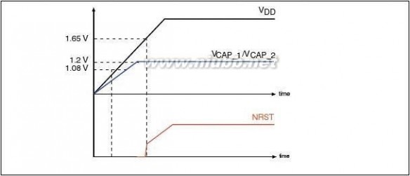
The regulator bypass/regulator off mode allows to supply externally a 1.2V voltage
source through VCAP_1 and VCAP_2 pins, in addition to VDD.
VDD minimum value is 1.8V.
The following conditions must be respected in Regulator bypass mode:
–
–VDD should always be higher than VCAP_1 and VCAP_2 to avoid current injection between power domains. If the time for VCAP_1 and VCAP_2 to reach 1.08V is faster than the time for VDD to
reach 1.8V, then PA0 should be connected to the NRST pin (see Figure6).
Otherwise, PA0 should be asserted low externally until VDD reaches 1.8V (see
Figure7).
In regulator bypass only mode, PA0 cannot be used as a GPIO pin.
●Regulator bypass/regulator off and internal reset off
This mode is activated by setting IRROFF pin to VDD. IRROFF cannot be activated in
conjunction with REGOFF. This mode is available only on the WLCSP package. It
allows to supply externally a 1.2V voltage source through VCAP_1 and VCAP_2 pins, in
addition to VDD.
VDD minimum value is 1.65V.
The following conditions must be respected in Regulator bypass mode (see Figure8):
–
–VDD should always be higher than VCAP_1 and VCAP_2 to avoid current injection between power domains. External reset should be used to cover both conditions: until VCAP_1 and VCAP_2 reach 1.08V and until VDD reaches 1.65V
PA0 can be used as a standard GPIO pin.
Doc ID 15818 Rev 521/147
205 STM32F205xx207xx参考手册
DescriptionFigure 6.STM32F205xx, STM32F207xxStartup in regulator bypass/regulator off mode: slow VDD slope

Figure 7.Startup in regulator bypass/regulator off mode: slow VDD slope

22/147Doc ID 15818 Rev 5
205 STM32F205xx207xx参考手册
STM32F205xx, STM32F207xxDescription
2.2.18 Real-time clock (RTC), backup SRAM and backup registers
The backup domain of the STM32F205xx and STM32F207xx includes:
●
●
●The real-time clock (RTC) 4 Kbytes of backup SRAM20 backup registers
The RTC provides a set of continuously running counters which can be used with suitable
software to provide a clock calendar function, an alarm interrupt and a periodic interrupt. It is
clocked by a 32.768 kHz external crystal, resonator or oscillator, the internal low-power RC
oscillator or the high-speed external clock divided by 128. The internal low-speed RC has a
typical frequency of 32 kHz. The RTC can be calibrated using an external 512 Hz output to
compensate for any natural quartz deviation.
The RTC features calendar registers with seconds, minutes, hours, week day, date, month,
year. Two alarm registers are used to generate an alarm at a specific time and calendar
fields can be independently masked for alarm comparison. To generate a periodic interrupt,
a 16-bit programmable binary auto-reload downcounter with programmable resolution is
available and allows automatic wakeup and periodic alarms from every 120 μs to every 36
hours.
A 20-bit prescaler is used for the time base clock. It is by default configured to generate a
time base of 1 second from a clock at 32.768 kHz.
The backup SRAM size is 4 Kbytes and can be enabled by software. When the backup RAM
is enabled the power consumption in Standby or VBAT mode is slightly higher (see
Section2.2.19: Low-power modes).
The backup registers are 32-bit registers used to store 80 bytes of user application data
when VDD power is not present. Backup registers are not reset by a system, a power reset,
or when the device wakes up from the Standby mode (see Section2.2.19: Low-power
modes).
The RTC, backup RAM and backup registers are supplied through a switch that takes power
from either the VDD supply when present or the VBAT pin.
2.2.19 Low-power modes
The STM32F205xx and STM32F207xx support three low-power modes to achieve the best
compromise between low power consumption, short startup time and available wakeup
sources:
●Sleep mode
In Sleep mode, only the CPU is stopped. All peripherals continue to operate and can
wake up the CPU when an interrupt/event occurs.
扩展:stm32f207参考手册 / stm32f205参考手册 / stm32f207编程参考
●Stop mode
The Stop mode achieves the lowest power consumption while retaining the contents of
SRAM and registers. All clocks in the 1.2 V domain are stopped, the PLL, the HSI RC
Doc ID 15818 Rev 523/147
205 STM32F205xx207xx参考手册
DescriptionSTM32F205xx, STM32F207xxand the HSE crystal oscillators are disabled. The voltage regulator can also be put
either in normal or in low-power mode.
The device can be woken up from the Stop mode by any of the EXTI line. The EXTI line
source can be one of the 16 external lines, the PVD output, the RTC alarm / wakeup /
tamper / time stamp events, the USB OTG FS/HS wakeup or the Ethernet wakeup.
●Standby mode
The Standby mode is used to achieve the lowest power consumption. The internal
voltage regulator is switched off so that the entire 1.2 V domain is powered off. The
PLL, the HSI RC and the HSE crystal oscillators are also switched off. After entering
Standby mode, the SRAM and register contents are lost except for registers in the
backup domain and the backup SRAM when selected.
The device exits the Standby mode when an external reset (NRST pin), an IWDG reset,
a rising edge on the WKUP pin, or an RTC alarm / wakeup / tamper /time stamp event
occurs.
Note:1The RTC, the IWDG, and the corresponding clock sources are not stopped when the device
enters the Stop or Standby mode.
2.2.20 VBAT operation
The VBAT pin allows to power the device VBAT domain from an external battery or an
external supercapacitor.
VBAT operation is activated when VDD is not present.
Note:When the microcontroller is supplied from VBAT, external interrupts and RTC alarm/events
do not exit it from VBAT operation.
2.2.21 Timers and watchdogs
The STM32F205xx and STM32F207xx devices include two advanced-control timers, eight
general-purpose timers, two basic timers and two watchdog timers.
Table3 compares the features of the advanced-control, general-purpose and basic timers.
Table 3.Timer feature comparison
DMA Capture/Max Max request compare interface timer outputgenerationchannelsclockclock
Yes4Yes60 MHz120
MHz
60
MHz
60
MHz
60
MHz Counter Counter Prescaler Timer typeTimerresolutiontypefactorAdvanced-TIM1, controlTIM8TIM2, TIM5TIM3, TIM4TIM6, TIM7Up, Any integer Down, between 1 Up/downand 65536Up, Any integer Down, between 1 Up/downand 65536Up, Any integer Down, between 1 Up/downand 65536UpAny integer between 1
and 6553616-bit32-bitYes4No30 MHzGeneral purpose16-bitYes4No30 MHzBasic16-bitYes0No30 MHz
24/147Doc ID 15818 Rev 5
205 STM32F205xx207xx参考手册
STM32F205xx, STM32F207xxTable 3.Timer feature comparison (continued)Description
Counter Counter Prescaler Timer typeTimerresolutiontypefactor
Any integer
between 1
and 65536
Any integer
between 1
and 65536
Any integer
between 1
and 65536
Any integer
between 1
and 65536DMA Capture/Max Max request compare interface timer outputgenerationchannelsclockclockNo2No60 MHz120 MHz120 MHz60 MHz60 MHzTIM916-bitUpGeneral purposeTIM10, TIM1116-bitUpNo1No60 MHzTIM1216-bitUpNo2No30 MHzTIM13, TIM1416-bitUpNo1No30 MHz
Advanced-control timers (TIM1, TIM8)
The advanced-control timers (TIM1, TIM8) can be seen as three-phase PWM generators multiplexed on 6 channels. They have complementary PWM outputs with programmable inserted dead times. They can also be considered as complete general-purpose timers. Their 4 independent channels can be used for:
●
●
●
●Input captureOutput comparePWM generation (edge- or center-aligned modes)One-pulse mode output
If configured as standard 16-bit timers, they have the same features as the general-purpose TIMx timers. If configured as 16-bit PWM generators, they have full modulation capability (0-100%).
The TIM1 and TIM8 counters can be frozen in debug mode. Many of the advanced-control timer features are shared with those of the standard TIMx timers which have the same architecture. The advanced-control timer can therefore work together with the TIMx timers via the Timer Link feature for synchronization or event chaining.
General-purpose timers (TIMx)
There are ten synchronizable general-purpose timers embedded in the STM32F20x devices (see Table3 for differences).
●TIM2, TIM3, TIM4, TIM5
The STM32F20x include 4 full-featured general-purpose timers. TIM2 and TIM5 are 32-bit timers, and TIM3 and TIM4 are 16-bit timers. The TIM2 and TIM5 timers are based on a 32-bit auto-reload up/downcounter and a 32-bit prescaler. The TIM3 and TIM4 timers are based on a 16-bit auto-reload up/downcounter and a 16-bit prescaler. They all feature 4 independent channels for input capture/output compare, PWM or one-pulse mode output. This gives up to 16 input capture/output compare/PWMs on the largest packages.Doc ID 15818 Rev 525/147
扩展:stm32f207参考手册 / stm32f205参考手册 / stm32f207编程参考
205 STM32F205xx207xx参考手册
DescriptionSTM32F205xx, STM32F207xxThe TIM2, TIM3, TIM4, TIM5 general-purpose timers can work together, or with the
other general-purpose timers and the advanced-control timers TIM1 and TIM8 via the
Timer Link feature for synchronization or event chaining.
The counters of TIM2, TIM3, TIM4, TIM5 can be frozen in debug mode. Any of these
general-purpose timers can be used to generate PWM outputs.
TIM2, TIM3, TIM4, TIM5 all have independent DMA request generation. They are
capable of handling quadrature (incremental) encoder signals and the digital outputs
from 1 to 4 hall-effect sensors.
●TIM10, TIM11 and TIM9
These timers are based on a 16-bit auto-reload upcounter and a 16-bit prescaler.
TIM10 and TIM11 feature one independent channel, whereas TIM9 has two
independent channels for input capture/output compare, PWM or one-pulse mode
output. They can be synchronized with the TIM2, TIM3, TIM4, TIM5 full-featured
general-purpose timers. They can also be used as simple time bases.
●TIM12, TIM13 and TIM14
These timers are based on a 16-bit auto-reload upcounter and a 16-bit prescaler.
TIM13 and TIM14 feature one independent channel, whereas TIM12 has two
independent channels for input capture/output compare, PWM or one-pulse mode
output. They can be synchronized with the TIM2, TIM3, TIM4, TIM5 full-featured
general-purpose timers.
They can also be used as simple time bases.
2.2.22 Basic timers TIM6 and TIM7
These timers are mainly used for DAC trigger and waveform generation. They can also be
used as a generic 16-bit time base.
2.2.23 Independent watchdog
The independent watchdog is based on a 12-bit downcounter and 8-bit prescaler. It is
clocked from an independent 32 kHz internal RC and as it operates independently from the
main clock, it can operate in Stop and Standby modes. It can be used either as a watchdog
to reset the device when a problem occurs, or as a free-running timer for application timeout
management. It is hardware- or software-configurable through the option bytes.
The counter can be frozen in debug mode.
2.2.24 Window watchdog
The window watchdog is based on a 7-bit downcounter that can be set as free-running. It
can be used as a watchdog to reset the device when a problem occurs. It is clocked from the
main clock. It has an early warning interrupt capability and the counter can be frozen in
debug mode.
26/147Doc ID 15818 Rev 5
205 STM32F205xx207xx参考手册
STM32F205xx, STM32F207xxDescription
2.2.25 SysTick timer
This timer is dedicated to real-time operating systems, but could also be used as a standard
downcounter. It features:
●●●●
A 24-bit downcounterAutoreload capability
Maskable system interrupt generation when the counter reaches 0Programmable clock source
2.2.26 I2C bus
Up to three I2C bus interfaces can operate in multimaster and slave modes. They can
support the Standard- and Fast-modes. They support the 7/10-bit addressing mode and the 7-bit dual addressing mode (as slave). A hardware CRC generation/verification is embedded.
They can be served by DMA and they support SMBus 2.0/PMBus.
2.2.27 Universal synchronous/asynchronous receiver transmitters
(UARTs/USARTs)
The STM32F205xx and STM32F207xx embed four universal synchronous/asynchronous receiver transmitters (USART1, USART2, USART3 and USART6) and two universal asynchronous receiver transmitters (UART4 and UART5).
These six interfaces provide asynchronous communication, IrDA SIR ENDEC support, multiprocessor communication mode, single-wire half-duplex communication mode and have LIN Master/Slave capability. The USART1 and USART6 interfaces are able to
communicate at speeds of up to 7.5 Mbit/s. The other available interfaces communicate at up to 3.75 Mbit/s.
USART1, USART2, USART3 and USART6 also provide hardware management of the CTS and RTS signals, Smart Card mode (ISO 7816 compliant) and SPI-like communication capability. All interfaces can be served by the DMA controller.
Table 4.
USART feature comparison
Max. baud rate Max. baud rate
Smartcard in Mbit/s in Mbit/s APB (ISO7816)(oversampling (oversampling mapping
by 16)by 8)
X
3.75
7.5
APB2
(max. 60MHz)APB1 (max. 30MHz)APB1 (max. 30MHz)
USART Modem SPI
LINirDA
namefeatures(RTS/CTS)master
USART1XXXXX
USART2XXXXXX1.873.75
USART3XXXXXX1.873.75
Doc ID 15818 Rev 527/147
205 STM32F205xx207xx参考手册
DescriptionTable 4.USART feature comparison (continued)STM32F205xx, STM32F207xxUSART Modem SPI LINirDAnamefeatures(RTS/CTS)masterMax. baud rate Max. baud rate Smartcard in Mbit/s in Mbit/s APB (ISO7816)(oversampling (oversampling mapping
扩展:stm32f207参考手册 / stm32f205参考手册 / stm32f207编程参考
by 16)by 8)
-1.873.75APB1 (max.
30MHz)
APB1
(max.
30MHz)
APB2
(max.
60MHz)UART4X-X-XUART5X-XD-X-3.753.75USART6XXXXXX3.757.5
2.2.28 Serial peripheral interface (SPI)
The STM32F20x feature up to three SPIs in slave and master modes in full-duplex and
simplex communication modes. SPI1 can communicate at up to 30 Mbits/s, SPI2 and SPI3 can communicate at up to 15 Mbit/s. The 3-bit prescaler gives 8 master mode frequencies and the frame is configurable to 8 bits or 16 bits. The hardware CRC generation/verification supports basic SD Card/MMC modes. All SPIs can be served by the DMA controller.
The SPI interface can be configured to operate in TI mode for communications in master
mode and slave mode.
2.2.29 Inter-integrated sound (I2S)
Two standard I2S interfaces (multiplexed with SPI2 and SPI3) are available. They can be
operated in master or slave mode, and can be configured to operate with a 16-/32-bit
resolution as input or output channels. Audio sampling frequencies from 8 kHz up to 96 kHz are supported. When either or both of the I2S interfaces is/are configured in master mode, the master clock can be output to the external DAC/CODEC at 256 times the sampling
frequency.
2.2.30 SDIO
An SD/SDIO/MMC host interface is available, that supports MultiMediaCard System
Specification Version 4.2 in three different databus modes: 1-bit (default), 4-bit and 8-bit.
The interface allows data transfer at up to 48 MHz in 8-bit mode, and is compliant with the SD Memory Card Specification Version 2.0.
The SDIO Card Specification Version 2.0 is also supported with two different databus
modes: 1-bit (default) and 4-bit.
The current version supports only one SD/SDIO/MMC4.2 card at any one time and a stack of MMC4.1 or previous.
In addition to SD/SDIO/MMC, this interface is fully compliant with the CE-ATA digital protocol Rev1.1.28/147Doc ID 15818 Rev 5
205 STM32F205xx207xx参考手册
STM32F205xx, STM32F207xxDescription
2.2.31 Ethernet MAC interface with dedicated DMA and IEEE1588 support
Peripheral available only on the STM32F207xx devices.
The STM32F207xx devices provide an IEEE-802.3-2002-compliant media access controller
(MAC) for ethernet LAN communications through an industry-standard medium-
independent interface (MII) or a reduced medium-independent interface (RMII). The
STM32F207xx requires an external physical interface device (PHY) to connect to the
physical LAN bus (twisted-pair, fiber, etc.). the PHY is connected to the STM32F207xx MII
port using 17 signals for MII or 9 signals for RMII, and can be clocked using the 25 MHz
(MII) or 50 MHz (RMII) output from the STM32F207xx.
The STM32F207xx includes the following features:
●
●Supports 10 and 100 Mbit/s ratesDedicated DMA controller allowing high-speed transfers between the dedicated SRAM and the descriptors (see the STM32F20x and STM32F21x reference manual for
details)
Tagged MAC frame support (VLAN support)
Half-duplex (CSMA/CD) and full-duplex operation
MAC control sublayer (control frames) support
32-bit CRC generation and removal
Several address filtering modes for physical and multicast address (multicast and group addresses)
32-bit status code for each transmitted or received frame
Internal FIFOs to buffer transmit and receive frames. The transmit FIFO and the receive FIFO are both 2 Kbytes, that is 4 Kbytes in total
Supports hardware PTP (precision time protocol) in accordance with IEEE 1588 2008 (PTP V2) with the time stamp comparator connected to the TIM2 input
Triggers interrupt when system time becomes greater than target time●●●●●●●●●
2.2.32 Controller area network (CAN)
The two CANs are compliant with the 2.0A and B (active) specifications with a bitrate up to 1
Mbit/s. They can receive and transmit standard frames with 11-bit identifiers as well as
extended frames with 29-bit identifiers. Each CAN has three transmit mailboxes, two receive
FIFOS with 3 stages and 28 shared scalable filter banks (all of them can be used even if one
CAN is used). The 256 bytes of SRAM which are allocated for each CAN are not shared
with any other peripheral.
2.2.33 Universal serial bus on-the-go full-speed (OTG_FS)
The STM32F205xx and STM32F207xx embed an USB OTG full-speed device/host/OTG
peripheral with integrated transceivers. The USB OTG FS peripheral is compliant with the
USB 2.0 specification and with the OTG 1.0 specification. It has software-configurable
endpoint setting and supports suspend/resume. The USB OTG full-speed controller
Doc ID 15818 Rev 529/147
205 STM32F205xx207xx参考手册
DescriptionSTM32F205xx, STM32F207xxrequires a dedicated 48 MHz clock that is generated by a PLL connected to the HSE
扩展:stm32f207参考手册 / stm32f205参考手册 / stm32f207编程参考
oscillator. The major features are:
●
●
●
●
●
●
●
●Combined Rx and Tx FIFO size of 320 × 35 bits with dynamic FIFO sizingSupports the session request protocol (SRP) and host negotiation protocol (HNP)4 bidirectional endpoints8 host channels with periodic OUT supportHNP/SNP/IP inside (no need for any external resistor)For OTG/Host modes, a power switch is needed in case bus-powered devices are connectedInternal FS OTG PHY support External FS OTG PHY support through an I2C connection
2.2.34 Universal serial bus on-the-go high-speed (OTG_HS)
The STM32F205xx and STM32F207xx devices embed a USB OTG high-speed (up to
480Mb/s) device/host/OTG peripheral. The USB OTG HS supports both full-speed and
high-speed operations. It integrates the transceivers for full-speed operation (12MB/s) and
features a UTMI low-pin interface (ULPI) for high-speed operation (480MB/s). When using
the USB OTG HS in HS mode, an external PHY device connected to the ULPI is required.
The USB OTG HS peripheral is compliant with the USB 2.0 specification and with the OTG
1.0 specification. It has software-configurable endpoint setting and supports
suspend/resume. The USB OTG full-speed controller requires a dedicated 48 MHz clock
that is generated by a PLL connected to the HSE oscillator. The major features are:
●
●
●
●
●
●
●Combined Rx and Tx FIFO size of 1 Kbit × 35 with dynamic FIFO sizingSupports the session request protocol (SRP) and host negotiation protocol (HNP)6 bidirectional endpoints12 host channels with periodic OUT supportInternal FS OTG PHY support External FS OTG PHY support through an I2C connectionExternal HS or HS OTG operation supporting ULPI in SDR mode. The OTG PHY is connected to the microcontroller ULPI port through 12 signals. It can be clocked using
the 60MHz output.
Internal USB DMA
HNP/SNP/IP inside (no need for any external resistor)
for OTG/Host modes, a power switch is needed in case bus-powered devices are connected●●●
2.2.35 Audio PLL (PLLI2S)
The devices feature an additional dedicated PLL for audio I2S application. It allows to
achieve error-free I2S sampling clock accuracy without compromising on the CPU
performance, while using USB peripherals.
The PLLI2S configuration can be modified to manage an I2S sample rate change without
disabling the main PLL (PLL) used for CPU, USB and Ethernet interfaces.
The audio PLL can be programmed with very low error to obtain sampling rates ranging
from 8KHz to 96KHz.
30/147Doc ID 15818 Rev 5
205 STM32F205xx207xx参考手册
STM32F205xx, STM32F207xxDescription
In addition to the audio PLL, a master clock input pin can be used to synchronize the I2S
flow with an external PLL (or Codec output).
2.2.36 Digital camera interface (DCMI)
The camera interface is not available in STM32F205xx devices.
STM32F207xx products embed a camera interface that can connect with camera modules
and CMOS sensors through an 8-bit to 14-bit parallel interface, to receive video data. The
camera interface can sustain up to 27 Mbyte/s at 27 MHz or 48Mbyte/s at 48 MHz. It
features:
●
●
●
●
●Programmable polarity for the input pixel clock and synchronization signalsParallel data communication can be 8-, 10-, 12- or 14-bitSupports 8-bit progressive video monochrome or raw bayer format, YCbCr 4:2:2 progressive video, RGB 565 progressive video or compressed data (like JPEG)Supports continuous mode or snapshot (a single frame) modeCapability to automatically crop the image
2.2.37 GPIOs (general-purpose inputs/outputs)
Each of the GPIO pins can be configured by software as output (push-pull or open-drain,
with or without pull-up or pull-down), as input (floating, with or without pull-up or pull-down)
or as peripheral alternate function. Most of the GPIO pins are shared with digital or analog
alternate functions. All GPIOs are high-current-capable and have speed selection to better
manage internal noise, power consumption and electromagnetic emission.
The I/O alternate function configuration can be locked if needed by following a specific
sequence in order to avoid spurious writing to the I/Os registers.
To provide fast I/O handling, the GPIOs are on the fast AHB1 bus with a clock up to
120MHz that leads to a maximum I/O toggling speed of 60 MHz.
2.2.38 ADCs (analog-to-digital converters)
Three 12-bit analog-to-digital converters are embedded and each ADC shares up to 16
external channels, performing conversions in the single-shot or scan mode. In scan mode,
automatic conversion is performed on a selected group of analog inputs.
Additional logic functions embedded in the ADC interface allow:
扩展:stm32f207参考手册 / stm32f205参考手册 / stm32f207编程参考
●
●Simultaneous sample and holdInterleaved sample and hold
The ADC can be served by the DMA controller. An analog watchdog feature allows very
precise monitoring of the converted voltage of one, some or all selected channels. An
interrupt is generated when the converted voltage is outside the programmed thresholds.
The events generated by the timers TIM1, TIM2, TIM3, TIM4, TIM5 and TIM8 can be
internally connected to the ADC start trigger and injection trigger, respectively, to allow the
application to synchronize A/D conversion and timers.
Doc ID 15818 Rev 531/147
205 STM32F205xx207xx参考手册
DescriptionSTM32F205xx, STM32F207xx2.2.39 DAC (digital-to-analog converter)
The two 12-bit buffered DAC channels can be used to convert two digital signals into two
analog voltage signal outputs. The design structure is composed of integrated resistor
strings and an amplifier in inverting configuration.
This dual digital Interface supports the following features:
●
●
●
●
●
●
●
●
●
●two DAC converters: one for each output channel8-bit or 12-bit monotonic outputleft or right data alignment in 12-bit modesynchronized update capabilitynoise-wave generationtriangular-wave generationdual DAC channel independent or simultaneous conversionsDMA capability for each channelexternal triggers for conversioninput voltage reference VREF+
Eight DAC trigger inputs are used in the device. The DAC channels are triggered through
the timer update outputs that are also connected to different DMA streams.
2.2.40 Temperature sensor
The temperature sensor has to generate a voltage that varies linearly with temperature. The
conversion range is between 1.8 V and 3.6 V. The temperature sensor is internally
connected to the ADC1_IN16 input channel which is used to convert the sensor output
voltage into a digital value.
As the offset of the temperature sensor varies from chip to chip due to process variation, the
internal temperature sensor is mainly suitable for applications that detect temperature
changes instead of absolute temperatures. If an accurate temperature reading is needed,
then an external temperature sensor part should be used.
2.2.41 Serial wire JTAG debug port (SWJ-DP)
The ARM SWJ-DP interface is embedded, and is a combined JTAG and serial wire debug
port that enables either a serial wire debug or a JTAG probe to be connected to the target.
The JTAG TMS and TCK pins are shared with SWDIO and SWCLK, respectively, and a
specific sequence on the TMS pin is used to switch between JTAG-DP and SW-DP.
2.2.42 Embedded Trace Macrocell?
The ARM Embedded Trace Macrocell provides a greater visibility of the instruction and data
flow inside the CPU core by streaming compressed data at a very high rate from the
STM32F20x through a small number of ETM pins to an external hardware trace port
analyzer (TPA) device. The TPA is connected to a host computer using USB, Ethernet, or
any other high-speed channel. Real-time instruction and data flow activity can be recorded
and then formatted for display on the host computer that runs the debugger software. TPA
hardware is commercially available from common development tool vendors.
The Embedded Trace Macrocell operates with third party debugger software tools.
32/147Doc ID 15818 Rev 5
205 STM32F205xx207xx参考手册
STM32F205xx, STM32F207xxPinouts and pin description
3 Pinouts and pin description
Figure 9.
STM32F20x LQFP64 pinout
0(????/3#?).0(????/3#?/54
.2340#??0#??0#??0#??633!6$$!0!????7+50
0!??0!??
64636261605958575655545352515049
481
472
463
454
445
436
427
418
,1&0????409
3910
3811
3712
3613
3514
3415
3316
6$$???????6#!0???0!????????0!????????0!????????0!????????0!??????0!??????0#??????0#??????0#??????0#??????0"????????0"????????0"????????0"??????
0!??633???6$$???0!??0!??0!??0!??0#??0#??0"??0"??0"??0"????0"????6#!0???6$$???
AI??????????B
1.Top view.
Doc ID 15818 Rev 533/147
205 STM32F205xx207xx参考手册
Pinouts and pin description
Figure 11.STM32F20x LQFP100 pinout
STM32F205xx, STM32F207xx
0%??0%??0%??0%??0%??6"!4
0#??????24#?!&??0#??????/3#?????).0#??????/3#?????/54
633???6$$???
0(????/3#?).0(????/3#?/54
.2340#??0#??0#??0#??6$$?????633!62%&??6$$!0!????7+50
0!??0!????????????????????????????????????????????????????????????????????????????????????
??????????????????????????????????????????????????????????????????????????????????????????????????????
????????????????????????????????????????????????????????????????????????????????????????????????????
扩展:stm32f207参考手册 / stm32f205参考手册 / stm32f207编程参考
6$$???2&50%??????0%??????0"??????0"??????"//4??????0"??????0"??????0"??????0"??????0"??????0$??????0$??????0$??????0$??????0$??????0$??????0$??????0$??????0#????????0#????????0#????????0!????????0!??????
,1&0??????
6$$?????633???6#!0???????0!??????????0!??????????0!??????????0!??????????0!????????0!????????0#??????0#??????0#??????0#??????0$????????0$????????0$????????0$????????0$????????0$????????0$??????0$??????0"????????0"????????0"????????0"????????
0!??633???6$$???0!??0!??0!??0!??0#??0#??0"??0"??0"??0%??0%??0%??0%????0%????0%????0%????0%????0%????0"????0"????6#!0???6$$???????????????????????????????????????????????????????????????????????????????????????????????????????
AI??????????D
1.RFU means “reserved for future use”.
34/147Doc ID 15818 Rev 5
205 STM32F205xx207xx参考手册
STM32F205xx, STM32F207xx
Pinouts and pin description
1.RFU means “reserved for future use”.
Doc ID 15818 Rev 5
35/147
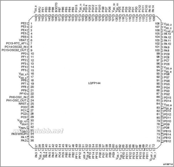
205 STM32F205xx207xx参考手册
Pinouts and pin description
STM32F205xx, STM32F207xx
1.Package not in production and available for development only.2.RFU means “reserved for future use”.
36/147Doc ID 15818 Rev 5
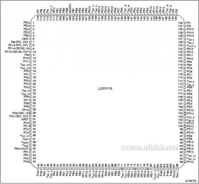
205 STM32F205xx207xx参考手册
STM32F205xx, STM32F207xx
Pinouts and pin description
1.RFU means “reserved for future use”.2.Top view.
Doc ID 15818 Rev 537/147
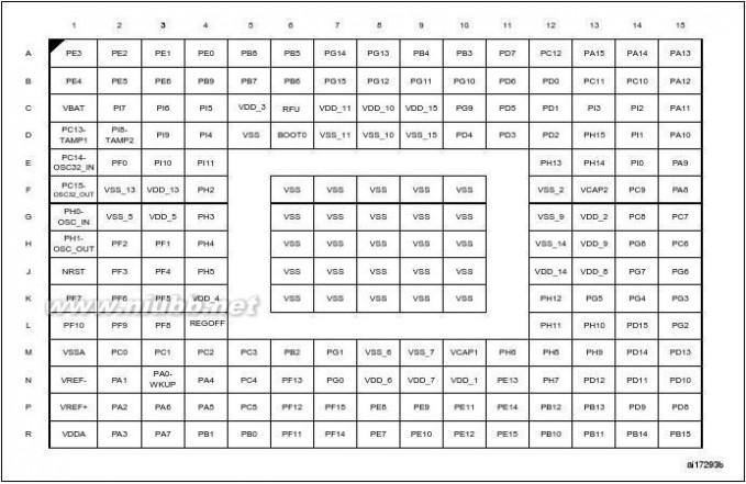
205 STM32F205xx207xx参考手册
Pinouts and pin descriptionTable 5.
WLCSP64+2
STM32F205xx, STM32F207xx
STM32F20x pin and ball definitions
I / O Level(2)
Pins
UFBGA176
Type(1)
LQFP100
LQFP144
LQFP176
Main function(3) (after reset)
LQFP64
Pin nameAlternate functions
Other functions
-----1-234-----------------
-----A9-B8B9C9-----------
123456-789-----------
123456-789-----
12345678910
A2A1B1B2B3C1D2D1
PE2PE3PE4PE5PE6VBATPI8(4)PC13(4)PC15(4)-OSC32_OUT(6)
PI9PI10PI11VSS_13VDD_13PF0PF1PF2PF3(6)PF4(6)PF5(6)VSS_5VDD_5PF6(6)PF7(6)PF8(6)PF9(6)
I/OFTI/OFTI/OFTI/OFTI/OFTSI/OFTI/OFT
PE2PE3PE4PE5PE6VBATPI8(5)PC13(5)PC14(5)PC15(5)PI9PI10PI11VSS_13VDD_13PF0PF1PF2PF3PF4PF5VSS_5VDD_5PF6PF7PF8PF9
TRACECLK/ FSMC_A23 /
ETH_MII_TXD3TRACED0/FSMC_A19TRACED1/FSMC_A20 /
DCMI_D4TRACED2 / FSMC_A21 / TIM9_CH1 / DCMI_D6TRACED3 / FSMC_A22 / TIM9_CH2 / DCMI_D7
RTC_AF2RTC_AF1OSC32_INOSC32_OUT
CAN1_RX ETH_MII_RX_EROTG_HS_ULPI_DIR
E1PC14(4)-OSC32_IN(6)I/OFTF1
I/OFTI/OFTI/OFTI/OFTSSI/OFTI/OFTI/OFTI/OFTI/OFTI/OFTSSI/OFTI/OFTI/OFTI/OFT
11D312E313E41415
F2F3
1016E21117H31218H213191420
J2J3
FSMC_A0 / I2C2_SDAFSMC_A1 / I2C2_SCLFSMC_A2 / I2C2_SMBA
FSMC_A3FSMC_A4FSMC_A5
ADC3_IN9ADC3_IN14ADC3_IN15
1521K3
H9101622G2-----111723G3----1824K21925K120262127
L3L2
TIM10_CH1 / FSMC_NIORDTIM11_CH1/FSMC_NREG
TIM13_CH1 / FSMC_NIOWRTIM14_CH1 / FSMC_CD
ADC3_IN4ADC3_IN5ADC3_IN6ADC3_IN7
38/147Doc ID 15818 Rev 5
205 STM32F205xx207xx参考手册
STM32F205xx, STM32F207xxTable 5.
WLCSP64+2
Pinouts and pin description
STM32F20x pin and ball definitions (continued)
I / O Level(2)
Pins
UFBGA176
Type(1)
LQFP100
LQFP144
LQFP176
Main function(3) (after reset)
LQFP64
Pin nameAlternate functions
Other functions
-56789
--2228L1
PF10(6)PH0(6)-OSC_INPH1(6)-OSC_OUT
NRSTPC0(6)PC1(6)
(6)
I/OFTI/OFTI/OFTI/OI/OFTI/OFT
PF10PH0PH1NRSTPC0PC1
FSMC_INTRADC3_IN8OSC_INOSC_OUT
E9122329G1F9132430H1E8142531
J1
OTG_HS_ULPI_STP
ETH_MDCSPI2_MISO / OTG_HS_ULPI_DIR / ETH_MII_TXD2SPI2_MOSI / I2S2_SD / OTG_HS_ULPI_NXT / ETH_MII_TX_CLK
ADC123_IN10ADC123_IN11ADC123_IN12ADC123_IN13
G9152632M2F8162733M3
10D7172834M4PC2I/OFTPC2
11G8182935M5-12--13
---193036
-
PC3
(6)
I/OFTSSSSS
PC3VDD_12VSSAVREF-VREF+VDDA
VDD_12VSSAVREF-VREF+VDDA
PA0(7)-WKUP(6)
203137M1---N1
F7213238P1-223339R1
14E7233440N3
USART2_CTS/ UART4_TX/
ETH_MII_CRS / ADC123_CH0
I/OFTPA0-WKUP
TIM2_CH1_ETR//WKUPTIM5_CH1 / TIM8_ETR
USART2_RTS / UART4_RX/
ETH_RMII_REF_CLK / ETH_MII_RX_CLK / TIM5_CH2 / TIM2_CH2
15H8243541N2
PA1(6)
I/OFTPA1ADC123_IN1
16J9253642P2----------------43
F4
PA2
(6)
I/OFTI/OFTI/OFTI/OFTI/OFT
PA2PH2PH3PH4PH5
扩展:stm32f207参考手册 / stm32f205参考手册 / stm32f207编程参考
USART2_TX/TIM5_CH3 /
TIM9_CH1 / TIM2_CH3 / ADC123_IN2
ETH_MDIO
ETH_MII_CRSETH_MII_COLI2C2_SCL / OTG_HS_ULPI_NXT
I2C2_SDA
PH2PH3PH4PH5
44G445H446
J4
Doc ID 15818 Rev 539/147
205 STM32F205xx207xx参考手册
Pinouts and pin descriptionTable 5.
WLCSP64+2
STM32F205xx, STM32F207xx
STM32F20x pin and ball definitions (continued)
I / O Level(2)
Pins
UFBGA176
Type(1)
LQFP100
LQFP144
LQFP176
Main function(3) (after reset)
LQFP64
Pin nameAlternate functions
Other functions
17G7263747R2
PA3(6)
I/OFTPA3
USART2_RX/TIM5_CH4 / TIM9_CH2 / TIM2_CH4 /
ADC123_IN3
OTG_HS_ULPI_D0 / ETH_MII_COL
18F1273848
H7
-L4
VSS_4REGOFFVDD_4PA4(6)
SI/OS
VSS_4REGOFFVDD_4PA4
SPI1_NSS / SPI3_NSS /
USART2_CK / DCMI_HSYNC / OTG_HS_SOF/ I2S3_WSSPI1_SCK/
OTG_HS_ULPI_CK / / TIM2_CH1_ETR/ TIM8_CHIN
ADC12_IN4 /DAC1_OUT
19E1283949K4
20J8294050N4I/O
21H6304151P4
PA5(6)
I/OPA5
ADC12_IN5/DAC2_OUT
22H5314252P3
PA6(6)
I/OFTPA6
SPI1_MISO /
TIM8_BKIN/TIM13_CH1 /
ADC12_IN6
DCMI_PIXCLK / TIM3_CH1
/ TIM1_BKINSPI1_MOSI/ TIM8_CH1N /
TIM14_CH1TIM3_CH2/
ADC12_IN7
ETH_MII_RX_DV / TIM1_CH1N / RMII_CRS_DVETH_RMII_RX_D0 / ETH_MII_RX_D0ETH_RMII_RX_D1 / ETH_MII_RX_D1
ADC12_IN14ADC12_IN15
23J7324353R3
PA7(6)FT
PA7
24H4334454N525G3344555P5
PC4(6)PC5(6)
I/OFTI/OFT
PC4PC5
26J6354656R5
PB0(6)
I/OFTPB0
TIM3_CH3 / TIM8_CH2N/ OTG_HS_ULPI_D1/
ADC12_IN8
ETH_MII_RXD2 / TIM1_CH2NTIM3_CH4 / TIM8_CH3N/ OTG_HS_ULPI_D2/ ETH_MII_RXD3 / ADC12_IN9 OTG_HS_INTN / TIM1_CH3N
27J5364757R4
PB1(6)
I/OFTPB1
28J4374858M6------4959R65060P6
PB2PF11PF12
I/OFTPB2-BOOT1I/OFTI/OFT
PF11PF12
DCMI_12FSMC_A6
40/147Doc ID 15818 Rev 5
205 STM32F205xx207xx参考手册
STM32F205xx, STM32F207xxTable 5.
WLCSP64+2
Pinouts and pin description
STM32F20x pin and ball definitions (continued)
I / O Level(2)
Pins
UFBGA176
Type(1)
LQFP100
LQFP144
LQFP176
Main function(3) (after reset)
LQFP64
Pin nameAlternate functions
Other functions
------------------
------------------
-------
5161M85262N85363N65464R75565P75666N75767M7
VSS_6VDD_6PF13PF14PF15PG0PG1PE7PE8PE9VSS_7VDD_7PE10PE11PE12PE13PE14PE15
SSI/OFTI/OFTI/OFTI/OFTI/OFTI/OFTI/OFTI/OFTSSI/OFTI/OFTI/OFTI/OFTI/OFTI/OFT
VSS_6VDD_6PF13PF14PF15PG0PG1PE7PE8PE9VSS_7VDD_7PE10PE11PE12PE13PE14PE15
FSMC_D7/TIM1_CH2NFSMC_D8/TIM1_CH2FSMC_D9/TIM1_CH3NFSMC_D10/TIM1_CH3FSMC_D11/TIM1_CH4FSMC_D12/TIM1_BKINSPI2_SCK/ I2S2_CK/ I2C2_SCL / USART3_TX / OTG_HS_ULPI_D3 / ETH_MII_RX_ER / OTG_HS_SCL / TIM2_CH3I2C2_SDA/USART3_RX/ OTG_HS_ULPI_D4 / ETH_RMII_TX_EN/ ETH_MII_TX_EN / OTG_HS_SDA / TIM2_CH4
FSMC_A7FSMC_A8FSMC_A9FSMC_A10FSMC_A11FSMC_D4/TIM1_ETRFSMC_D5/TIM1_CH1NFSMC_D6/TIM1_CH1
385868R8395969P8406070P9--6171M96272N9
416373R9426474P10436575R10446676N11456777P11466878R11
29H3476979R12PB10I/OFTPB10
30J2487080R13PB11I/OFTPB11
31J3497181M1032-------507282N10------83M1184N1285M12
VCAP_1VDD_1PH6PH7PH8
SSI/OFTI/OFTI/OFT
VCAP_1VDD_1PH6PH7PH8
I2C2_SMBA / TIM12_CH1 /
ETH_MII_RXD2
I2C3_SCL / ETH_MII_RXD3I2C3_SDA / DCMI_HSYNC
Doc ID 15818 Rev 541/147
205 STM32F205xx207xx参考手册
Pinouts and pin descriptionTable 5.
WLCSP64+2
STM32F205xx, STM32F207xx
STM32F20x pin and ball definitions (continued)
I / O Level(2)
Pins
UFBGA176
Type(1)
LQFP100
LQFP144
LQFP176
Main function(3) (after reset)
LQFP64
Pin nameAlternate functions
Other functions
------
------
------
------
86M1387L1388L1289K1290H1291J12
PH9PH10PH11PH12VSS_14VDD_14
I/OFTI/OFTI/OFTI/OFTSS
PH9PH10PH11PH12VSS_14VDD_14
I2C3_SMBA / TIM12_CH2/
DCMI_D0
TIM5_CH1_ETR /
DCMI_D1TIM5_CH2 / DCMI_D2TIM5_CH3 / DCMI_D3
33J1517392P12PB12I/OFTPB12
SPI2_NSS/I2S2_WS/
I2C2_SMBA/
USART3_CK/ TIM1_BKIN /
CAN2_RX / OTG_HS_ULPI_D5/ ETH_RMII_TXD0 / ETH_MII_TXD0/ OTG_HS_IDSPI2_SCK / I2S2_CK /
USART3_CTS/
TIM1_CH1N /CAN2_TX / OTG_HS_ULPI_D6 / ETH_RMII_TXD1 / ETH_MII_TXD1SPI2_MISO/ TIM1_CH2N / TIM12_CH1 / OTG_HS_DM
USART3_RTS/ TIM8_CH2NSPI2_MOSI / I2S2_SD / TIM1_CH3N / TIM8_CH3N
/ TIM12_CH2 / OTG_HS_DPFSMC_D13 / USART3_TXFSMC_D14 / USART3_RXFSMC_D15 / USART3_CKFSMC_A16/USART3_CTSFSMC_A17/TIM4_CH1 /
USART3_RTSFSMC_A18/TIM4_CH2
34H2527493P13PB13I/OFTPB13
OTG_HS_VBUS
35H1537594R14PB14I/OFTPB14
36G1547695R15PB15I/OFTPB15
扩展:stm32f207参考手册 / stm32f205参考手册 / stm32f207编程参考
--------
--------
557796P15567897P14577998N15588099N145981100N136082101M15--83102
-
PD8PD9PD10PD11PD12PD13VSS_8VDD_8
I/OFTI/OFTI/OFTI/OFTI/OFTI/OFTSS
PD8PD9PD10PD11PD12PD13VSS_8VDD_8
84103J13
42/147Doc ID 15818 Rev 5
205 STM32F205xx207xx参考手册
STM32F205xx, STM32F207xxTable 5.
WLCSP64+2
Pinouts and pin description
STM32F20x pin and ball definitions (continued)
I / O Level(2)
Pins
UFBGA176
Type(1)
LQFP100
LQFP144
LQFP176
Main function(3) (after reset)
LQFP64
Pin nameAlternate functions
Other functions
-----------
-----------
6185104M146286105L14---------87106L1588107K1589108K1490109K1391110J1592111J1493112H1494113G1295114H13
PD14PD15PG2PG3PG4PG5PG6PG7PG8VSS_9VDD_9PC6
I/OFTI/OFTI/OFTI/OFTI/OFTI/OFTI/OFTI/OFTI/OFTSS
PD14PD15PG2PG3PG4PG5PG6PG7PG8VSS_9VDD_9PC6
FSMC_D0/TIM4_CH3FSMC_D1/TIM4_CH4
FSMC_A12FSMC_A13FSMC_A14FSMC_A15FSMC_INT2
FSMC_INT3 /USART6_CK
USART6_RTS / ETH_PPS_OUT
37G26396115H15I/OFT
SPI2_MCK /
TIM8_CH1/SDIO_D6 /
USART6_TX / DCMI_D0/TIM3_CH1SPI3_MCK /
TIM8_CH2/SDIO_D7 /
USART6_RX / DCMI_D1/TIM3_CH2TIM8_CH3/SDIO_D0 /TIM3_CH3/ USART6_CK /
DCMI_D2I2S2_CKIN/ I2S3_CKIN/
MCO2 /
TIM8_CH4/SDIO_D1 / /I2C3_SDA / DCMI_D3 /
TIM3_CH4MCO1 / USART1_CK/ TIM1_CH1/ I2C3_SCL/
OTG_FS_SOFUSART1_TX/ TIM1_CH2 / I2C3_SMBA / DCMI_D0USART1_RX/ TIM1_CH3/ OTG_FS_ID/DCMI_D1USART1_CTS / CAN1_RX / TIM1_CH4 / OTG_FS_DM
OTG_FS_VBUS
38F26497116G15PC7I/OFTPC7
39F36598117G14PC8I/OFTPC8
40D16699118F14PC9I/OFTPC9
41E267100119F15PA8I/OFTPA8
42E368101120E1543D369102121D1544D270103122C15
PA9PA10PA11
I/OFTI/OFTI/OFT
PA9PA10PA11
Doc ID 15818 Rev 543/147
205 STM32F205xx207xx参考手册
Pinouts and pin descriptionTable 5.
WLCSP64+2
STM32F205xx, STM32F207xx
STM32F20x pin and ball definitions (continued)
I / O Level(2)
Pins
UFBGA176
Type(1)
LQFP100
LQFP144
LQFP176
Main function(3) (after reset)
LQFP64
Pin nameAlternate functions
Other functions
45C171104123B1546B272105124A1547C273106125F13-B174107126F12
PA12PA13VCAP_2VSS_2VDD_2PH13PH14PH15PI0PI1PI2PI3VSS_15VDD_15PA14
I/OFTI/OFTSSSI/OFTI/OFTI/OFTI/OFTI/OFTI/OFTI/OFTSSI/OFT
PA12JTMS-SWDIOVCAP_2VSS_2VDD_2PH13PH14PH15PI0PI1PI2PI3VSS_15VDD_15JTCK-SWCLKJTDI
USART1_RTS / CAN1_TX/ TIM1_ETR/ OTG_FS_DP
JTMS-SWDIO
48A875108127G13----------------------------128E12-129E13-130D13-131E14-132D14-133C14-134C13-135D9-136C9
TIM8_CH1N / CAN1_TXTIM8_CH2N / DCMI_D4TIM8_CH3N / DCMI_D11TIM5_CH4 / SPI2_NSS / I2S2_WS / DCMI_D13SPI2_SCK / I2S2_CK /
DCMI_D8TIM8_CH4 /SPI2_MISO /
DCMI_D9TIM8_ETR / SPI2_MOSI / I2S2_SD / DCMI_D10
49A176109137A14JTCK-SWCLKJTDI/ SPI3_NSS/
I2S3_WS/TIM2_CH1_ETR
/ SPI1_NSSSPI3_SCK / I2S3_CK / UART4_TX / SDIO_D2 / DCMI_D8 / USART3_TXUART4_RX/ SPI3_MISO /
SDIO_D3 /
DCMI_D4/USART3_RXUART5_TX/SDIO_CK / DCMI_D9 / SPI3_MOSI / I2S3_SD / USART3_CKFSMC_D2/CAN1_RXFSMC_D3 / CAN1_TX
50A277110138A13I/OFT
51B378111139B14PC10I/OFTPC10
52C379112140B13PC11I/OFTPC11
53A380113141A12----81114142B1282115143C12
PC12PD0PD1
I/OFTI/OFTI/OFT
PC12PD0PD1
44/147Doc ID 15818 Rev 5
205 STM32F205xx207xx参考手册
STM32F205xx, STM32F207xxTable 5.
WLCSP64+2
Pinouts and pin description
STM32F20x pin and ball definitions (continued)
I / O Level(2)
Pins
UFBGA176
Type(1)
LQFP100
LQFP144
LQFP176
Main function(3) (after reset)
LQFP64
Pin nameAlternate functions
Other functions
54C783116144D12----------------------84117145D1185118146D1086119147C11-120148D8-121149C887122150B1188123151A11-124152C10-125153B10-126154B9-127155B8
PD2PD3PD4PD5VSS_10VDD_10PD6PD7PG9PG10PG11PG12
I/OFTI/OFTI/OFTI/OFTSSI/OFTI/OFTI/OFTI/OFTI/OFTI/OFT
PD2PD3PD4PD5VSS_10VDD_10PD6PD7PG9PG10PG11PG12
TIM3_ETR/UART5_RXSDIO_CMD / DCMI_D11FSMC_CLK/USART2_CTSFSMC_NOE/USART2_RTSFSMC_NWE/USART2_TX
FSMC_NWAIT/USART2_R
XUSART2_CK/FSMC_NE1/F
SMC_NCE2USART6_RX /
FSMC_NE2/FSMC_NCE3
FSMC_NCE4_1/ FSMC_NE3FSMC_NCE4_2 / ETH_MII_TX_ENFSMC_NE4 / USART6_RTSFSMC_A24 / USART6_CTS
/ETH_MII_TXD0/ETH_RMII
_TXD0FSMC_A25 / USART6_TX/ETH_MII_TXD1/ETH_RMII
_TXD1
---128156A8PG13I/OFTPG13
----
----
-129157A7-130158D7-131159C7-132160B7
PG14VSS_11VDD_11PG15PB3
I/OFTSSI/OFT
PG14VSS_11VDD_11PG15
USART6_CTS / DCMI_D13JTDO/ TRACESWO/ SPI3_SCK / I2S3_CK / TIM2_CH2 / SPI1_SCKNJTRST/ SPI3_MISO / TIM3_CH1 / SPI1_MISO
55A489133161A10
JTDO/
I/OFT
TRACESWOI/OFT
NJTRST
扩展:stm32f207参考手册 / stm32f205参考手册 / stm32f207编程参考
56B490134162A9PB4
Doc ID 15818 Rev 545/147
205 STM32F205xx207xx参考手册
Pinouts and pin descriptionTable 5.
WLCSP64+2
STM32F205xx, STM32F207xx
STM32F20x pin and ball definitions (continued)
I / O Level(2)
Pins
UFBGA176
Type(1)
LQFP100
LQFP144
LQFP176
Main function(3) (after reset)
LQFP64
Pin nameAlternate functions
Other functions
57A591135163A6PB5I/OFTPB5
I2C1_SMBA/ CAN2_RX / OTG_HS_ULPI_D7 / / SPI1_MOSI/ SPI3_MOSI / DCMI_D10 / I2S3_SDI2C1_SCL/ TIM4_CH1 / CAN2_TX /OTG_FS_INTN / DCMI_D5/USART1_TXI2C1_SDA / FSMC_NL(8) /
DCMI_VSYNC / USART1_RX/ TIM4_CH2
VPP
TIM4_CH3/SDIO_D4/ TIM10_CH1 / DCMI_D6 /
OTG_FS_SCL/ ETH_MII_TXD3 / I2C1_SCL/ CAN1_RXSPI2_NSS/ I2S2_WS/ TIM4_CH4/ TIM11_CH1/ OTG_FS_SDA/ SDIO_D5 / DCMI_D7 / I2C1_SDA /
CAN1_TXTIM4_ETR / FSMC_NBL0 /
DCMI_D2FSMC_NBL1 / DCMI_D3
58B592136164B6PB6I/OFTPB6
59A693137165B560B694138166D6
PB7BOOT0
I/OFTI
PB7BOOT0
61B795139167A5PB8I/OFTPB8
62A796140168B4PB9I/OFTPB9
--
---
97141169A498142170A3
D5
----
PE0PE1VSSVSS_3RFU(9)VDD_3PI4PI5PI6PI7IRROFF
I/OFTI/OFTSS
PE0PE1VSSVSS_3VDD_3PI4PI5PI6PI7IRROFF
63D8--
99143171C6
64D9100144172C5---------C8
------173D4-174C4-175C3-176C2---
SI/OFTI/OFTI/OFTI/OFTI/O
TIM8_BKIN / DCMI_D5TIM8_CH1 / DCMI_VSYNCTIM8_CH2 / DCMI_D6TIM8_CH3 / DCMI_D7
1.I = input, O = output, S = supply, HiZ = high impedance.2.FT = 5 V tolerant.
3.Function availability depends on the chosen device.
46/147Doc ID 15818 Rev 5
205 STM32F205xx207xx参考手册
STM32F205xx, STM32F207xxPinouts and pin description
4.PC13, PC14, PC15 and PI8 are supplied through the power switch. Since the switch only sinks a limited amount of current (3mA), the use of GPIOs PC13 to PC15 and PI8 in output mode is limited: the speed should not exceed 2 MHz with a maximum load of 30 pF and these I/Os must not be used as a current source (e.g. to drive an LED).
5.Main function after the first backup domain power-up. Later on, it depends on the contents of the RTC registers even after reset (because these registers are not reset by the main reset). For details on how to manage these I/Os, refer to the RTC register description sections in the STM32F20x and STM32F21x reference manual, available from the STMicroelectronics website: www.st.com.
6.FT = 5 V tolerant except when in analog mode or oscillator mode (for PC14, PC15, PH0 and PH1).
7.If the device is delivered in an UFBGA176 package and if the REGOFF pin is set to VDD (Regulator in bypass mode), then PA0 is used as an internal Reset (active low).
8.FSMC_NL pin is also named FSMC_NADV on memory devices.
9.RFU = reserved for future use.
Doc ID 15818 Rev 547/147
205 STM32F205xx207xx参考手册
48/147Table 6.Alternate function mapping
AF0AF1AF2AF3AF4AF5AF6AF7AF8AF9AF10AF11AF12AF13
Port
SYSTIM1/2TIM3/4/5TIM8/9/10/11SPI3/I2S3USART1/2/3UART4/5/FSMC/SDIO/AF014AF15
I2C1/I2C2/I2C3SPI1/SPI2/I2S2CAN1/CAN2/
USART6TIM12/13/14ETHOTG_FSDCMI
PA0-WKUPTIM2_CH1
TIM2_ETR TIM 5_CH1TIM8_ETR USART2_CTS UART4_TX ETH_MII_CRS EVENTOUT
PA1ETH_MII _RX_CLK
ETH_RMII _REF_CLKEVENTOUT
PA2ETH_MDIOEVENTOUTPA3OTG_HS_ULPI_DETH EVENTOUTPA4SPI1_NSS SPI3_NSS
I2S3_WS USART2_CK OTG_HS_SOFPA5TIM2_CH1
TIM2_ETR EVENTOUT
PA6EVENTOUTPA7ETH_MII _RX_DV
ETH_RMII _CRS_DVEVENTOUT
PA8MCO1EVENTOUTPA9CMI_Doc ID 15818 Rev 5PA10TIM1_CH3 CMI_EVENTOUT
PA11TIM1_CH4 OTG_FS_MEVENTOUTPA12TIM1_ETR OTG_FS_PEVENTOUTPA13EVENTOUTPA14EVENTOUTPA15JTDI TIM 2_CH1
TIM 2_ETR SPI1_NSS SPI3_NSS
I2S3_WS EVENTOUT
PB0OTG_HS_ULPI_D_MII_RXDEVENTOUTPB1OTG_HS_ULPI_D_MII_RXDEVENTOUTPB2EVENTOUTPB3JTDO/
TRACESWOSPI3_SCK
I2S3_CK EVENTOUT
PB4SPI3_MISOEVENTOUTPB5SPI3_MOSI
I2S3_SD DDCMI_DEVENTOUT
PB6CMI_DEVENTOUTPB7EVENTOUTPB8_MII_TXDDSDIO_CMI_DEVENTOUTPB9I2C1_SDSPI2_NSS
I2S2_WS DDSDIO_CMI_DEVENTOUT
PB10I2S2_CK MII_RX_EREVENTOUT
PB11OTG_HS_ULPI_ETH _RMII_TX_ENOTG_HS_SPB12SPI2_NSS
I2S2_WS OTG_HS_ULPI_ETH _MII_TXD0
ETH _RMII_TXD0OTG_HS_IDEVENTOUT
PB13TIM1_CH1N SPI2_SCK
I2S2_CK OTG_HS_ULPI_ETH _MII_TXD1
ETH _RMII_TXD1PB14SPI2_MISOOTG_HS_EVENTOUTPinouts and pin descriptionSTM32F205xx, STM32F207xx
205 STM32F205xx207xx参考手册
Table 6.Alternate function mapping (continued)
AF0AF1AF2AF3AF4AF5AF6AF7AF8AF9AF10AF11AF12AF13
PortCAN1/CAN2/AF014AF15
SYSTIM1/2TIM3/4/5TIM8/9/10/11I2C1/I2C2/I2C3SPI1/SPI2/I2S2SPI3/I2S3USART1/2/3UART4/5/
USART6TIM12/13/14ETHFSMC/SDIO/
OTG_FSDCMI
PB15I2S2_SD EVENTOUT
PC0PC1ETH_MDCEVENTOUTPC2SPI2_MISOOTG_HS_ULPI_D_MII_TXDEVENTOUTPC3SPI2_MOSIETH _MII_TX_CLK
扩展:stm32f207参考手册 / stm32f205参考手册 / stm32f207编程参考
ETH _RMII_TX_CLK EVENTOUT
PC4ETH_MII_RXD0
ETH_RMII_RXD0EVENTOUT
PC5ETH _RMII_RXD1EVENTOUT
PC6SDIO_DCMI_EVENTOUTPC7SDIO_DCMI_EVENTOUTPC8IO_CMI_EVENTOUTPC9MCO2I2C3_SDI2S2_CKINDSIO_DCMI_EVENTOUTDoc ID 15818 Rev 5PC10SPI3_SCK
I2S3_CK DSIO_DDCMI_DEVENTOUT
PC11SPI3_MISODSIO_DDCMI_DEVENTOUTPC12SPI3_MOSI
I2S3_SD DSDCMI_DEVENTOUT
PC13
PC14-OSC32_IN
PC15-OSC32_OUT
PD0EVENTOUTPD1EVENTOUTPD2TIM3_ETR IO_CMCMI_EVENTOUTPD3USART2_CTS PD4USART2_RTS PD5USART2_TX PD6USART2_RX PD7USART2_CK PD8USART3_TX FSMC_PD9USART3_RX FSMC_PD10USART3_CK FSMC_PD11USART3_CTS PD12TIM4_CH1 USART3_RTS 49/147PD13TIM4_CH2 PD14TIM4_CH3 FSMC_STM32F205xx, STM32F207xxPinouts and pin description
205 STM32F205xx207xx参考手册
50/147Table 6.Alternate function mapping (continued)
AF0AF1AF2AF3AF4AF5AF6AF7AF8AF9AF10AF11AF12AF13
PortAF014AF15
SYSTIM1/2TIM3/4/5TIM8/9/10/11I2C1/I2C2/I2C3SPI1/SPI2/I2S2SPI3/I2S3USART1/2/3UART4/5/CAN1/CAN2/
USART6TIM12/13/14ETHFSMC/SDIO/
OTG_FSDCMI
PD15TIM4_CH4 FSMC_PE0TIM4_ETR CMI_DEVENTOUTPE1CMI_DEVENTOUTPE2TRACECLK ETH _MII_TXD3 FSMC_A23 EVENTOUTPE3TRACED0 PE4TRACED1 DCMI_EVENTOUTPE5TRACEDCMI_EVENTOUTPE6TRACEDCMI_EVENTOUT
PE7TIM1_ETR FSMC_PE8TIM1_CH1N FSMC_PE9TIM1_CH1 FSMC_PE10TIM1_CH2N FSMC_Doc ID 15818 Rev 5PE11TIM1_CH2 FSMC_PE12TIM1_CH3N FSMC_PE13TIM1_CH3 FSMC_PE14TIM1_CH4 FSMC_PE15TIM1_BKIN FSMC_PF0I2C2_SDA PF1I2C2_SCL PF2I2C2_SMBAPF3PF4PF5PF6TIM10_CH1 FSMC_NIORPF7TIM11_CH1 PF8EVENTOUTPF9EVENTOUTPF10PF11CMI_PF12PF13PF14PF15Pinouts and pin descriptionSTM32F205xx, STM32F207xx
205 STM32F205xx207xx参考手册
Table 6.Alternate function mapping (continued)
AF0AF1AF2AF3AF4AF5AF6AF7AF8AF9AF10AF11AF12AF13
Port
SYSTIM1/2TIM3/4/5TIM8/9/10/11SPI3/I2S3USART1/2/3UART4/5/FSMC/SDIO/AF014AF15
I2C1/I2C2/I2C3SPI1/SPI2/I2S2CAN1/CAN2/
USART6TIM12/13/14ETHOTG_FSDCMI
PG0PG1PG2PG3PG4PG5PG6PG7EVENTOUTPG8EVENTOUTPG9EVENTOUTPG10Doc ID 15818 Rev 5PG11ETH _MII_TX_EN
ETH _RMII_TX_ENPG12EVENTOUTPG13UART6_CTS ETH _MII_TXD0
ETH _RMII_TXD0PG14USART6_TX ETH _MII_TXD1
ETH _RMII_TXD1 PG15USART6_CTS CMI_PH0 - OSC_IN
PH1 - OSC_OUT
PH2ETH _MII_CRSEVENTOUTPH3ETH _MII_COL EVENTOUTPH4I2C2_SCL PH5I2C2_SDA EVENTOUTPH6I2C2_SMBA_MII_RXEVENTOUTPH7I2C3_SCL ETH _MII_RXD3 EVENTOUTPH8I2C3_SDA PH9I2C3_SMBACMI_EVENTOUTPH10TIM5_CH1TIM5_ETR CMI_PH11TIM5_CH2 CMI_PH12TIM5_CH3 CMI_PH13TIM8_CH1N CAN1_TXEVENTOUT51/147PH14TIM8_CH2N CMI_PH15TIM8_CH3N CMI_STM32F205xx, STM32F207xxPinouts and pin description
205 STM32F205xx207xx参考手册
52/147Table 6.Alternate function mapping (continued)
AF0AF1AF2AF3AF4AF5AF6AF7AF8AF9AF10AF11AF12AF13
Port
SYSTIM1/2TIM3/4/5TIM8/9/10/11SPI3/I2S3USART1/2/3UART4/5/CAN1/CAN2/FSMC/SDIO/AF014AF15
I2C1/I2C2/I2C3SPI1/SPI2/I2S2USART6TIM12/13/14ETHOTG_FSDCMI
PI0TIM5_CH4 I2S2_WS CMI_PI1SPI2_SCK
I2S2_CK CMI_PI2CMI_PI3TIM8_ETR SPI2_MOSI
I2S2_SD CMI_PI4TIM8_BKIN CMI_PI5TIM8_CH1 PI6TIM8_CH2 CMI_PI7TIM8_CH3 CMI_PI8
PI9CAN1_RXEVENTOUTPI10ETH _MII_RX_EREVENTOUT
Doc ID 15818 Rev 5PI11OTG_HS_ULPI_Pinouts and pin descriptionSTM32F205xx, STM32F207xx
205 STM32F205xx207xx参考手册
STM32F205xx, STM32F207xxMemory mapping
4 Memory mapping
The memory map is shown in Figure15.
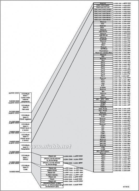
Doc ID 15818 Rev 553/147
205 STM32F205xx207xx参考手册
Electrical characteristicsSTM32F205xx, STM32F207xx5 Electrical characteristics
5.1 Parameter conditions
Unless otherwise specified, all voltages are referenced to VSS.
5.1.1 Minimum and maximum values
Unless otherwise specified the minimum and maximum values are guaranteed in the worst
conditions of ambient temperature, supply voltage and frequencies by tests in production on
100% of the devices with an ambient temperature at TA = 25 °C and TA = TAmax (given by
the selected temperature range).
Data based on characterization results, design simulation and/or technology characteristics
are indicated in the table footnotes and are not tested in production. Based on
characterization, the minimum and maximum values refer to sample tests and represent the
mean value plus or minus three times the standard deviation (mean±3Σ).
5.1.2 Typical values
Unless otherwise specified, typical data are based on TA = 25 °C, VDD = 3.3 V (for the
1.8V≤VDD≤3.6V voltage range). They are given only as design guidelines and are not tested.
Typical ADC accuracy values are determined by characterization of a batch of samples from
a standard diffusion lot over the full temperature range, where 95% of the devices have an
error less than or equal to the value indicated (mean±2Σ).
5.1.3 Typical curves
扩展:stm32f207参考手册 / stm32f205参考手册 / stm32f207编程参考
Unless otherwise specified, all typical curves are given only as design guidelines and are
not tested.
5.1.4 Loading capacitor
The loading conditions used for pin parameter measurement are shown in Figure16.
5.1.5 Pin input voltage
The input voltage measurement on a pin of the device is described in Figure17.
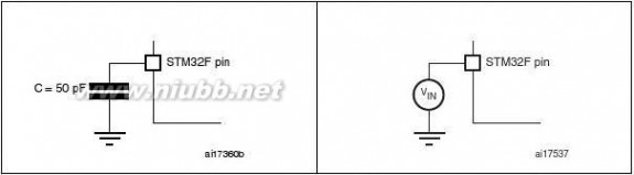
54/147Doc ID 15818 Rev 5
205 STM32F205xx207xx参考手册
STM32F205xx, STM32F207xxElectrical characteristics
5.1.6 Power supply scheme
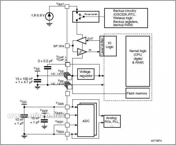
1.4.7μF capacitor must be connected to one of the VDD pin.
5.1.7 Current consumption measurement
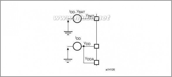
Doc ID 15818 Rev 555/147
205 STM32F205xx207xx参考手册
Electrical characteristicsSTM32F205xx, STM32F207xx
5.2 Absolute maximum ratings
Stresses above the absolute maximum ratings listed in Table7: Voltage characteristics, Table8: Current characteristics, and Table9: Thermal characteristics may cause permanent damage to the device. These are stress ratings only and functional operation of the device at these conditions is not implied. Exposure to maximum rating conditions for extended periods may affect device reliability.Table 7.
SymbolVDD–VSS
VIN|ΔVDDx||VSSX ? VSS|VESD(HBM)
Voltage characteristics
Ratings
External main supply voltage (including VDDA, VDD)(1)
Input voltage on five-volt tolerant pin(2)Input voltage on any other pin(3)
Variations between different VDD power pinsVariations between all the different ground pinsElectrostatic discharge voltage (human body model)
MinTBDVSS–0.3VSS–0.3
MaxTBDVDD+4.04.0TBDTBD
see Section5.3.13:
Absolute maximum ratings (electrical sensitivity)
mVVUnit
1.All main power (VDD, VDDA) and ground (VSS, VSSA) pins must always be connected to the external power
supply, in the permitted range.2.IINJ(PIN) must never be exceeded (see Table8: Current characteristics). This is implicitly insured if VIN
maximum is respected. If VIN maximum cannot be respected, the injection current must be limited
externally to the IINJ(PIN) value. A positive injection is induced by VIN> VINmax while a negative injection is induced by VIN < VSS. 3.Positive current injection is not possible on these I/Os. VIN maximum must be respected. Negative current
injection is possible and must not exceed IINJ(PIN).
Table 8.
SymbolIVDDIVSSIIO
(2)
Current characteristics
Ratings
Total current into VDD/VDDA power lines (source)(1)Total current out of VSS ground lines (sink)(1)Output current sunk by any I/O and control pinOutput current source by any I/Os and control pinInjected current on five-volt tolerant I/O(3)Injected current on any other pin(4)
Total injected current (sum of all I/O and control pins)(5)
Max.TBDTBDTBDTBD–5/+0±5TBD
mAUnit
IINJ(PIN)
ΣIINJ(PIN)(4)
1.All main power (VDD, VDDA) and ground (VSS, VSSA) pins must always be connected to the external power
supply, in the permitted range.2.Negative injection disturbs the analog performance of the device. See note in Section5.3.18: 12-bit ADC
characteristics.3.Positive injection is not possible on these I/Os. VIN maximum must always be respected. IINJ(PIN) must
never be exceeded. A negative injection is induced by VIN<VSS.4.IINJ(PIN) must never be exceeded. This is implicitly insured if VIN maximum is respected. If VIN maximum
cannot be respected, the injection current must be limited externally to the IINJ(PIN) value. A positive injection is induced by VIN > VDD while a negative injection is induced by VIN < VSS.
56/147Doc ID 15818 Rev 5
205 STM32F205xx207xx参考手册
STM32F205xx, STM32F207xxElectrical characteristics
5.When several inputs are submitted to a current injection, the maximum ΣIINJ(PIN) is the absolute sum of the
positive and negative injected currents (instantaneous values). These results are based on characterization with ΣIINJ(PIN) maximum current injection on four I/O port pins of the device.
Table 9.
Thermal characteristics
Ratings
Storage temperature rangeMaximum junction temperature
Value–40 to +125
125
Unit°C°C
SymbolTSTGTJ
5.3 Operating conditions
5.3.1
General operating conditions
Table 10.
SymbolfHCLKfPCLK1fPCLK2VDD
General operating conditions
Parameter
Internal AHB clock frequencyInternal APB1 clock frequencyInternal APB2 clock frequencyStandard operating voltageAnalog operating voltage
扩展:stm32f207参考手册 / stm32f205参考手册 / stm32f207编程参考
(ADC limited to 1 M samples)Analog operating voltage(ADC limited to 2 M samples)Backup operating voltage
LQFP64WLCSP66
Power dissipation at TA = 85°C LQFP100for suffix 6 or TA = 105°C for
LQFP144suffix 7(4)
LQFP176UFBGA176
Ambient temperature for 6
suffix version
Maximum power dissipation Low power dissipation
(5)
ConditionsMin0 0 0 1.8(1)
Max12030603.63.6
Unit
MHz
V
VDDA(2)
Must be the same potential as VDD(3)
1.8(1)2.41.65
V
3.63.6444392434500526513
–40
85
°CmWV
VBAT
PD
TA
Ambient temperature for 7 suffix version
TJ
Junction temperature range
–40
105
Maximum power dissipation Low power dissipation(5)6 suffix version7 suffix version
–40 –40
105125
°C
°C
1.This value is reduced to 1.65 V for STM32F20x in WLCSP package assuming IRROFF is set to VDD.2.When the ADC is used, refer to Table59: ADC characteristics.
3.It is recommended to power VDD and VDDA from the same source. A maximum difference of 300mV
between VDD and VDDA can be tolerated during power-up and operation.
Doc ID 15818 Rev 557/147
205 STM32F205xx207xx参考手册
Electrical characteristicsSTM32F205xx, STM32F207xx
4.If TA is lower, higher PD values are allowed as long as TJ does not exceed TJmax.
5.In low power dissipation state, TA can be extended to this range as long as TJ does not exceed TJmax.
Table 11.
Operating power supply range
Limitations depending on the operating power supply range
Maximum Flash memory access frequency (fFlashmax)16MHz with no Flash memory wait
state18MHz with no Flash memory wait
state
Number of wait
states at maximum CPU frequency (fCPUmax=120MHz)(1)
FSMC controller operation
Possible Flash memory operations
ADC operation
I/O operation
VDD =1.8 to 2.1V(2)
Conversion time up to 1Msps
7(3)
–Degraded speed
performanceup to 30MHz–No I/O
compensation
–Degraded speed
performanceup to 30MHz–No I/O
compensation
–Degraded speed
performance
up to 48MHz
–I/O
compensation works
8-bit erase and program operations only
VDD = 2.1 to 2.4V
Conversion time up to 1Msps
6
(3)
16-bit erase and program operations
VDD = 2.4 to 2.7V
Conversion time up to 2Msps
24MHz with no Flash memory wait
state
4
(3)
16-bit erase and program operations
VDD = 2.7 to 3.6V(4)
Conversion time up to 2Msps
30MHz with no Flash memory wait
state
3(3)
–up to 60MHz
–Full-speed
when VDD =
operation
3.0 to 3.6V32-bit erase
and program –I/O
–up to
operationscompensation
48MHz
works
when VDD = 2.7 to 3.0V
1.The number of wait states can be reduced by reducing the CPU frequency (see Figure20).
2.This voltage range is reduced to 1.65 to 2.1V for devices in WLCSP package assuming IRROFF is set to VDD.
3.Thanks to the ART accelerator and the 128-bit Flash memory, the number of wait states given here does not impact the
execution speed from Flash memory since the ART accelerator allows to achieve a performance equivalent to 0 wait state program execution.4.The voltage range for ULPI USB high-speed, Ethernet MII and Ethernet RMII is 3.0 to 3.6V.
58/147Doc ID 15818 Rev 5
205 STM32F205xx207xx参考手册
STM32F205xx, STM32F207xxElectrical characteristics
5.3.2 Operating conditions at power-up / power-down
(regulator not bypassed)
Subject to general operating conditions for TA.Table 12.
SymboltVDD
Operating conditions at power-up / power-down (regulator not bypassed)
Parameter
VDD rise time rateVDD fall time rate
MinTBDTBD
Max
Unitμs/V
∞∞
Doc ID 15818 Rev 559/147

205 STM32F205xx207xx参考手册
Electrical characteristicsSTM32F205xx, STM32F207xx
5.3.3
Operating conditions at power-up / power-down in regulatorbypass mode
Subject to general operating conditions for TA.Table 13.
SymboltVDD
Operating conditions at power-up / power-down in regulator bypass mode
Parameter
VDD rise time rateVDD fall time rate
Conditions
Power-upPower-down
MinTBDTBDTBDTBD
Max
Unit
∞∞∞∞
μs/V
tVCAP
VCAP_1 and VCAP_2 rise
Power-up
time rate
VCAP_1 and VCAP_2 fall time rate
Power-down
5.3.4 Embedded reset and power control block characteristics
The parameters given in Table14 are derived from tests performed under ambient temperature and VDD supply voltage conditions summarized in Table10.Table 14.
扩展:stm32f207参考手册 / stm32f205参考手册 / stm32f207编程参考
Symbol
Embedded reset and power control block characteristics
Parameter
Conditions
PLS[2:0]=000 (rising edge)PLS[2:0]=000 (falling edge)PLS[2:0]=001 (rising edge)PLS[2:0]=001 (falling edge)PLS[2:0]=010 (rising edge)PLS[2:0]=010 (falling edge)PLS[2:0]=011 (rising edge)
MinTBDTBDTBDTBDTBDTBDTBDTBDTBDTBDTBDTBDTBDTBDTBDTBD
Typ TBD2.00TBD2.20TBD2.30TBD2.50TBD2.70TBD2.80TBD2.90TBD3.00100
MaxTBDTBDTBDTBDTBDTBDTBDTBDTBDTBDTBDTBDTBDTBDTBDTBD
UnitVVVVVVVVVVVVVVVVmV
VPVD
Programmable voltage PLS[2:0]=011 (falling edge)detector level selectionPLS[2:0]=100 (rising edge)
PLS[2:0]=100 (falling edge)PLS[2:0]=101 (rising edge)PLS[2:0]=101 (falling edge)PLS[2:0]=110 (rising edge)PLS[2:0]=110 (falling edge)PLS[2:0]=111 (rising edge)PLS[2:0]=111 (falling edge)
VPVDhyst(2)
PVD hysteresis
60/147Doc ID 15818 Rev 5
205 STM32F205xx207xx参考手册
STM32F205xx, STM32F207xx
Table 14.
SymbolVPOR/PDR
Electrical characteristics
Embedded reset and power control block characteristics (continued)
Parameter
Conditions
MinTBD(1)TBDTBDTBDTBDTBDTBD
Typ 1.701.742.20TBD2.50TBD2.8040
TBD-TBD-TBD200MaxTBDTBDTBDTBDTBDTBDTBD
UnitVVVVVVVmVmsmA
Power-on/power-down Falling edgereset thresholdRising edgeBrownout level 1 threshold Brownout level 2 thresholdBrownout level 3 thresholdPDR hysteresis
Falling edgeRising edgeFalling edgeRising edgeFalling edge
VBOR1
VBOR2VBOR3VPDRhyst(2)
TRSTTEMPO(2)Reset temporization
IRUSH
InRush current on voltage regulator power-on
1.The product behavior is guaranteed by design down to the minimum VPOR/PDR value.2.Guaranteed by design, not tested in production.
5.3.5 Supply current characteristics
The current consumption is a function of several parameters and factors such as the operating voltage, ambient temperature, I/O pin loading, device software configuration, operating frequencies, I/O pin switching rate, program location in memory and executed binary code.
The current consumption is measured as described in Figure19: Current consumption measurement scheme.
All run mode current consumption measurements given in this section are performed with a reduced code that gives a consumption equivalent to Dhrystone 2.1 code.
Doc ID 15818 Rev 561/147
205 STM32F205xx207xx参考手册
Electrical characteristicsSTM32F205xx, STM32F207xx
Typical and maximum current consumption
The MCU is placed under the following conditions:
●●●
All I/O pins are in input mode with a static value at VDD or VSS (no load).All peripherals are disabled except if it is explicitly mentioned.
The Flash access time is adjusted to fHCLK frequency (0 wait state from 0 to 30MHz, 1 wait state from 30 to 60MHz, 2 wait states from 60 to 90MHz and 3 wait states from 90 to 120MHz).
Prefetch and Cache ON (Reminder: this bit must be set before clock setting and bus prescaling).
When the peripherals are enabled fPCLK1 = fHCLK/4, fPCLK2 = fHCLK/2, fADCCLK = fPCLK2/4
The maximum values are obtained for VDD = 3.6V and maximum ambient temperature (TA), and the typical values for TA= 25°C and VDD = 3.3V unless otherwise specified.
●●●
Table 15.
Typical and maximum current consumption in Run mode, code with data processingrunning from Flash
Typical
Max(1)
Unit
TA = 25°CTBDTBDTBDTBDTBDTBDTBDTBDTBDTBDTBDTBD
TA = 85°CTBDTBDTBDTBDTBDTBDTBDTBDTBDTBDTBDTBD
TA = 105°C
TBDTBDTBDTBDTBDTBDTBDTBDTBDTBDTBDTBD
mA
Parameter
Conditions
fHCLK120 MHz90 MHz
External clock(2), all 60 MHzperipherals enabled30 MHz
26 MHz
Symbol
IDD
Supply current in Run mode
16 MHz120 MHz90 MHz
External clock(2), all 60 MHzperipherals disabled30 MHz
26 MHz16 MHz
1.Based on characterization, not tested in production.2.External clock is 8 MHz and PLL is on when fHCLK > 8 MHz.
62/147Doc ID 15818 Rev 5
205 STM32F205xx207xx参考手册
STM32F205xx, STM32F207xxTable 16.
Electrical characteristics
Typical and maximum current consumption in Run mode, code with data processing running from RAM
Typ
Max(1)
Unit
TA = 25°C49.5382614.5TBDTBD221712.57TBDTBD
TA = 85°CTBDTBDTBDTBDTBDTBDTBDTBDTBDTBDTBDTBD
TA = 105°C
TBDTBDTBDTBDTBDTBDTBDTBDTBDTBDTBDTBD
mA
Parameter
Conditions
fHCLK120 MHz90 MHz
60 MHzExternal clock(2),
all peripherals enabled(3)30 MHz
26 MHz
Supply current in Run mode
External clock(2), all peripherals disabled
Symbol
IDD
16 MHz120 MHz90 MHz60 MHz30 MHz26 MHz16 MHz
1.Based on characterization, tested in production at VDD max, fHCLK max.2.External clock is 8 MHz and PLL is on when fHCLK > 8 MHz.
扩展:stm32f207参考手册 / stm32f205参考手册 / stm32f207编程参考
3.Add an additional power consumption of 0.8 mA per ADC for the analog part. In applications, this consumption occurs only
while the ADC is on (ADON bit is set in the ADC_CR2 register).
Table 17.
Symbol
Typical and maximum current consumption in Sleep mode
Typ
Parameter
Conditions
fHCLK120 MHz90 MHz
60 MHzExternal clock(2),
(3)all peripherals enabled30 MHz
26 MHz16 MHz120 MHz90 MHz
External clock(2), all
peripherals disabled
60 MHz30 MHz26 MHz16 MHz
Max(1)
TA = 105°CTBDTBDTBDTBDTBDTBDTBDTBDTBDTBDTBDTBD
mAUnit
TA = 25°CTA = 85°C37.529.520.514.5TBDTBD8.06.55.03.5TBDTBD
TBDTBDTBDTBDTBDTBDTBDTBDTBDTBDTBDTBD
IDD
Supply current in Sleep mode
1.Based on characterization, tested in production at VDD max and fHCLK max with peripherals enabled.2.External clock is 8 MHz and PLL is on when fHCLK > 8 MHz.
Doc ID 15818 Rev 563/147
205 STM32F205xx207xx参考手册
Electrical characteristicsSTM32F205xx, STM32F207xx
3.Add an additional power consumption of 0.8 mA per ADC for the analog part. In applications, this consumption occurs only
while the ADC is on (ADON bit is set in the ADC_CR2 register).
Table 18.
Symbol
Typical and maximum current consumptions in Stop mode
Typ(1)
Parameter
Conditions
Max
VDD/VBATVDD/VBATVDD/VBATTA = TA = Unit= 1.8V= 2.4V= 3.3V85°C105°C
Flash in Stop mode, low-speed and high-speed internal RC oscillators
Supply current and high-speed oscillator OFF (no in Stop mode independent watchdog)with main Flash in Deep power down mode, regulator in low-speed and high-speed internal Run modeRC oscillators and high-speed
IDD_STOP
oscillator OFF (no independent
watchdog)
Flash in Stop mode, low-speed and high-speed internal RC oscillators
Supply current and high-speed oscillator OFF (no in Stop mode independent watchdog)with main
regulator in Flash in Deep power down mode,
low-speed and high-speed internal Low Power
RC oscillators and high-speed mode
oscillator OFF (no independent watchdog)
350TBDTBD
300TBDTBD
μA
200
150
1.Typical values are measured at TA = 25 °C.
Table 19.
Symbol
Typical and maximum current consumptions in Standby mode
Typ(1)
Parameter
Conditions
Max
VDD/VBATVDD/VBATVDD/VBATTA = TA = Unit= 1.8V= 2.4V= 3.3V85°C105°C
43.33.22.5
TBDTBDTBDTBDTBD(2)TBD(2)TBD(2)TBD(2)
μA
Backup SRAM ON, RTC ON
Supply current Backup SRAM OFF, RTC ON
IDD_STBYin Standby
Backup SRAM ON, RTC OFFmode
Backup SRAM OFF, RTC OFF
1.Typical values are measured at TA = 25 °C.2.Based on characterization, not tested in production.
64/147Doc ID 15818 Rev 5
205 STM32F205xx207xx参考手册
STM32F205xx, STM32F207xxTable 20.
Symbol
Electrical characteristics
Typical and maximum current consumptions in VBAT mode
Typ(1)
Parameter
Conditions
Max
VDD/VBATVDD/VBATVDD/VBATTA = TA = Unit= 1.8V= 2.4V= 3.3V85°C105°C
0.81.500.7
TBD(2)TBD(2)TBDTBDTBDTBDTBDTBDμA
Backup
IDD_VBATdomain supply Backup SRAM ON, RTC ON
current Backup SRAM OFF, RTC OFF
Backup SRAM ON, RTC OFF
1.Typical values are measured at TA = 25 °C.2.Based on characterization, not tested in production.
Backup SRAM OFF, low-speed
oscillator and RTC ON
On-chip peripheral current consumption
The current consumption of the on-chip peripherals is given in Table21. The MCU is placed under the following conditions:
●●●
all I/O pins are in input mode with a static value at VDD or VSS (no load)all peripherals are disabled unless otherwise mentioned
the given value is calculated by measuring the current consumption––
with all peripherals clocked off
with one peripheral clocked on (with only the clock applied)
●
ambient operating temperature and VDD supply voltage conditions summarized in Table7.
Peripheral current consumption
Peripheral(1)
GPIO AGPIO BGPIO CGPIO DGPIO E
Typical consumption at 25 °C
TBDTBDTBDTBDTBDTBDTBDTBDTBDTBDTBDTBDTBDTBD
mAUnit
Table 21.
AHB1GPIO FGPIO GGPIO HGPIO IOTG_HSETH_MACOTG_FS
AHB2DCMIRNG
Doc ID 15818 Rev 565/147
205 STM32F205xx207xx参考手册
Electrical characteristics
Table 21.
Peripheral current consumption (continued)
Peripheral(1)
TIM2TIM3TIM4TIM5TIM6TIM7TIM12TIM13TIM14USART2
APB1
USART3UART4UART5I2C1I2C2I2C3SPI2SPI3CAN1CAN2DACSDIOTIM1TIM8TIM9TIM10
APB2
TIM11ADC1(2)ADC2(2)ADC3SPI1USART1USART6
STM32F205xx, STM32F207xx
Typical consumption at 25 °C
TBDTBDTBDTBDTBDTBDTBDTBDTBDTBDTBDTBDTBDTBDTBDTBDTBDTBDTBDTBDTBDTBDTBDTBDTBDTBDTBDTBDTBDTBDTBDTBDTBD
扩展:stm32f207参考手册 / stm32f205参考手册 / stm32f207编程参考
Unit
mA
mA
1.fHCLK = 120 MHz, fAPB1 = fHCLK/4, fAPB2 = fHCLK/2, default prescaler value for each peripheral.
2.Specific conditions for ADC: fHCLK = 120MHz, fAPB1 = fHCLK/4, fAPB2 = fHCLK/2, fADCCLK = fAPB2/2, ADON
bit in the ADC_CR2 register is set to 1.
66/147Doc ID 15818 Rev 5
205 STM32F205xx207xx参考手册
STM32F205xx, STM32F207xxElectrical characteristics
5.3.6 External clock source characteristics
High-speed external user clock generated from an external source
The characteristics given in Table22 result from tests performed using an high-speed
external clock source, and under ambient temperature and supply voltage conditions summarized in Table10.Table 22.
SymbolfHSE_extVHSEHVHSELtw(HSE)tw(HSE)tr(HSE)tf(HSE)Cin(HSE)
High-speed external user clock characteristics
Parameter
External user clock source frequency(1)
OSC_IN input pin high level voltageOSC_IN input pin low level voltageOSC_IN high or low time(1)OSC_IN rise or fall time(1)OSC_IN input capacitance(1)
45
VSS≤VIN≤VDD
5
55±1
Conditions
Min10.7VDDVSS16
ns
20
pF%μA
Typ8
Max50VDD0.3VDD
UnitMHzV
DuCy(HSE)Duty cycle
IL
OSC_IN Input leakage current
1.Guaranteed by design, not tested in production.
Low-speed external user clock generated from an external source
The characteristics given in Table23 result from tests performed using an low-speed external clock source, and under ambient temperature and supply voltage conditions summarized in Table10.Table 23.
SymbolfLSE_extVLSEHVLSELtw(LSE)tw(LSE)tr(LSE)tf(LSE)Cin(LSE)
Low-speed external user clock characteristics
Parameter
User External clock source frequency(1)
OSC32_IN input pin high level voltage
OSC32_IN input pin low level voltage
OSC32_IN high or low time(1)OSC32_IN rise or fall time(1)OSC32_IN input capacitance(1)
30
5
70±1
0.7VDDVSS450
ns
50
pF%μA
Conditions
Min
Typ32.768
Max1000VDD
V
0.3VDD
UnitkHz
DuCy(LSE)Duty cycle
IL
OSC32_IN Input leakage current VSS≤VIN≤VDD
1.Guaranteed by design, not tested in production.
Doc ID 15818 Rev 567/147
205 STM32F205xx207xx参考手册
Electrical characteristicsSTM32F205xx, STM32F207xx
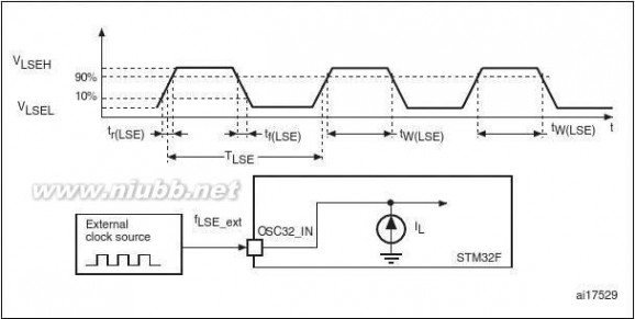
High-speed external clock generated from a crystal/ceramic resonator
The high-speed external (HSE) clock can be supplied with a 4 to 26 MHz crystal/ceramic
resonator oscillator. All the information given in this paragraph are based on characterization
results obtained with typical external components specified in Table24. In the application,
the resonator and the load capacitors have to be placed as close as possible to the oscillator
pins in order to minimize output distortion and startup stabilization time. Refer to the crystal
resonator manufacturer for more details on the resonator characteristics (frequency,
package, accuracy).
68/147Doc ID 15818 Rev 5
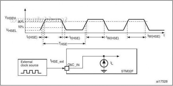
205 STM32F205xx207xx参考手册
STM32F205xx, STM32F207xx
Table 24.
SymbolfOSC_INRFC
Electrical characteristics
HSE 4-26 MHz oscillator characteristics(1) (2)
Parameter
Oscillator frequencyFeedback resistor
Recommended load capacitance versus equivalent serial
resistance of the crystal (RS)(3)HSE driving currentOscillator transconductance
RS = 30 ΩVDD = 3.3 V, VIN=VSS
with 30 pF load
Startup VDD is stabilized
25
2
Conditions
Min4
20030Typ
Max26
UnitMHzkΩ pF
i2gm
1mAmA/Vms
tSU(HSE(4)Startup time
2.Based on characterization, not tested in production.
1.Resonator characteristics given by the crystal/ceramic resonator manufacturer.
3.The relatively low value of the RF resistor offers a good protection against issues resulting from use in a
humid environment, due to the induced leakage and the bias condition change. However, it is recommended to take this point into account if the MCU is used in tough humidity conditions.4.tSU(HSE) is the startup time measured from the moment it is enabled (by software) to a stabilized 8 MHz
oscillation is reached. This value is measured for a standard crystal resonator and it can vary significantly with the crystal manufacturer
For CL1 and CL2, it is recommended to use high-quality external ceramic capacitors in the 5pF to 25pF range (typ.), designed for high-frequency applications, and selected to match the requirements of the crystal or resonator (see Figure23). CL1 and CL2 are usually the same size. The crystal manufacturer typically specifies a load capacitance which is the series combination of CL1 and CL2. PCB and MCU pin capacitance must be included (10pF can be used as a rough estimate of the combined pin and board capacitance) when sizing CL1 and CL2. Refer to the application note AN2867 “Oscillator design guide for ST microcontrollers” available from the ST website www.st.com.
扩展:stm32f207参考手册 / stm32f205参考手册 / stm32f207编程参考
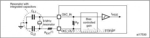
1.REXT value depends on the crystal characteristics.
Low-speed external clock generated from a crystal/ceramic resonator
The low-speed external (LSE) clock can be supplied with a 32.768 kHz crystal/ceramic resonator oscillator. All the information given in this paragraph are based on characterization results obtained with typical external components specified in Table25. In the application, the resonator and the load capacitors have to be placed as close as possible to the oscillator pins in order to minimize output distortion and startup stabilization time. Refer to the crystal resonator manufacturer for more details on the resonator characteristics (frequency, package, accuracy).
Doc ID 15818 Rev 569/147
205 STM32F205xx207xx参考手册
Electrical characteristics
Table 25.
SymbolRFC
(2)
STM32F205xx, STM32F207xx
LSE oscillator characteristics (fLSE = 32.768 kHz) (1)
Parameter
Feedback resistor
Recommended load capacitance versus equivalent serial
resistance of the crystal (RS)(3)LSE driving current
Oscillator Transconductance
VDD is stabilizedRS = 30 kΩVDD = 3.3 V, VIN = VSS
5
3
Conditions
Min
Typ5
151.4Max
UnitMΩ pFμAμA/Vs
I2gm
tSU(LSE)(4)startup time
1.Based on characterization, not tested in production.
2.Refer to the note and caution paragraphs below the table, and to the application note AN2867 “Oscillator
design guide for ST microcontrollers”.3.The oscillator selection can be optimized in terms of supply current using an high quality resonator with
small RS value for example MSIV-TIN32.768kHz. Refer to crystal manufacturer for more details4.tSU(LSE) is the startup time measured from the moment it is enabled (by software) to a stabilized
32.768kHz oscillation is reached. This value is measured for a standard crystal resonator and it can vary significantly with the crystal manufacturer
Note:
For CL1 and CL2 it is recommended to use high-quality external ceramic capacitors in the 5pF to 15pF range selected to match the requirements of the crystal or resonator (see Figure24). CL1 and CL2, are usually the same size. The crystal manufacturer typically specifies a load capacitance which is the series combination of CL1 and CL2.
Load capacitance CL has the following formula: CL = CL1 x CL2 / (CL1 + CL2) + Cstray where Cstray is the pin capacitance and board or trace PCB-related capacitance. Typically, it is between 2 pF and 7 pF.
To avoid exceeding the maximum value of CL1 and CL2 (15 pF) it is strongly recommended to use a resonator with a load capacitance CL≤ 7 pF. Never use a resonator with a load capacitance of 12.5 pF.
Example: if you choose a resonator with a load capacitance of CL = 6 pF, and Cstray = 2 pF, then CL1 = CL2 = 8 pF.
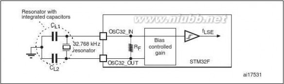
Caution:
70/147Doc ID 15818 Rev 5
205 STM32F205xx207xx参考手册
STM32F205xx, STM32F207xxElectrical characteristics
5.3.7 Internal clock source characteristics
The parameters given in Table26 are derived from tests performed under ambient temperature and VDD supply voltage conditions summarized in Table10.
High-speed internal (HSI) RC oscillator
Table 26.
SymbolfHSI
HSI oscillator characteristics (1)
Parameter
Conditions
Min
Typ
Max
Unit
User-trimmed with the RCC_CR register(2)
TBD
TBDTBDTBDTBDTBD
80
TBDTBDTBDTBDTBDTBD
%%%%%μsμA
ACCHSI
Accuracy of the HSI oscillatorFactory-calibrated
TA = –40 to 105°CTA = –10 to 85°CTA = 0 to 70°CTA = 25°C
tsu(HSI)IDD(HSI)
HSI oscillator startup timeHSI oscillator
power consumption
1.VDD = 3.3V, TA = –40 to 105°C unless otherwise specified.
2.Refer to application note AN2868 “STM32F10xxx internal RC oscillator (HSI) calibration” available from the
ST website www.st.com.
Low-speed internal (LSI) RC oscillator
Table 27.
SymbolfLSI(2)tsu(LSI)(3)IDD(LSI)(3)
Frequency
LSI oscillator startup timeLSI oscillator power consumption
LSI oscillator characteristics (1)
Parameter
Min30
Typ32850.65
Max60TBDTBD
UnitkHz μsμA
1.VDD = 3 V, TA = –40 to 105 °C unless otherwise specified.2.Based on characterization, not tested in production.3.Guaranteed by design, not tested in production.
5.3.8 Wakeup time from low-power mode
The wakeup times given in Table28 is measured on a wakeup phase with a 16MHz HSI RC oscillator. The clock source used to wake up the device depends from the current operating mode:
●●
Stop or Standby mode: the clock source is the RC oscillator
扩展:stm32f207参考手册 / stm32f205参考手册 / stm32f207编程参考
Sleep mode: the clock source is the clock that was set before entering Sleep mode.
All timings are derived from tests performed under ambient temperature and VDD supply voltage conditions summarized in Table10.
Doc ID 15818 Rev 571/147
205 STM32F205xx207xx参考手册
Electrical characteristics
Table 28.
STM32F205xx, STM32F207xx
Low-power mode wakeup timings
Parameter
Wakeup from Sleep mode
Wakeup from Stop mode (regulator in run mode)
Typ1915110200
μsμsUnitμs
SymboltWUSLEEP(1)
tWUSTOP(1)
Wakeup from Stop mode (regulator in low power mode)Wakeup from Stop mode (regulator in low power mode and Flash memory in Deep power down mode)Wakeup from Standby mode
tWUSTDBY(1)
1.The wakeup times are measured from the wakeup event to the point in which the user application code
reads the first instruction.
5.3.9 PLL characteristics
The parameters given in Table29 and Table30 are derived from tests performed under
temperature and VDD supply voltage conditions summarized in Table10.
Table 29.
SymbolfPLL_INfPLL_OUTfPLL48_OUTfVCO_OUTtLOCKJitterIDD(PLL)IDDA(PLL)
Main PLL characteristics
Parameter
PLL input clock(2)
PLL multiplier output clock48 MHz PLL multiplier output clockPLL VCO outputPLL lock timeCycle-to-cycle jitter
PLL power consumption on VDDPLL power consumption on VDDA
System clock 120MHzVCO freq = 192MHzVCO freq = 432MHzVCO freq = 192MHzVCO freq = 432MHz
TBCTBC192
Conditions
Min(1)Typ(1)0.9524
1
Max(1)2.0012048432350300TBCTBC
UnitMHzMHzMHzMHzμspsmAmA
1.Based on characterization, not tested in production.
2.Take care of using the appropriate division factor M to obtain the specified PLL input clock values. The M factor is shared
between PLL and PLLI2S.
Table 30.
SymbolfPLLI2S_INfPLLI2S_OUTfVCO_OUTtLOCKJitter
PLLI2S (audio PLL) characteristics
Parameter
PLLI2S input clock(2)
PLLI2S multiplier output clockPLLI2S VCO outputPLLI2S lock timeCycle-to-cycle jitter
System clock 120MHz
192
Conditions
Min(1)Typ(1)0.95
1
Max(1)1.05216432350300
UnitMHzMHzMHzμsps
72/147Doc ID 15818 Rev 5
205 STM32F205xx207xx参考手册
STM32F205xx, STM32F207xxTable 30.
Symbol
Electrical characteristics
PLLI2S (audio PLL) characteristics (continued)
Parameter
Conditions
Cycle to cycle at 12,343KHz
on 48KHz periodN=432, P=4, R=5Average frequency of 12,343KHz
N=432, P=4, R=5on 256 samplesCycle to cycle at 48KHzon 1000 samplesCycle to cycle at 50MHzon 1000 samplesCycle to cycle at 1MHzon 1000 samplesVCO freq = 192MHzVCO freq = 432MHzVCO freq = 192MHzVCO freq = 432MHz
Min(1)Typ(1)
Max(1)
Unit
JitterMaster I2S clock jitterTBCTBCps
JitterMaster I2S clock jitterTBCTBCps
JitterJitterJitterIDD(PLLI2S)IDDA(PLLI2S)
WS I2S clock jitter
Main Clock Output for EthernetBit Time CAN Jitter
PLLI2S power consumption on VDD
PLLI2S power consumption on VDDA
TBCTBCTBCTBCTBC
TBCTBCTBCTBCTBC
pspspsmAmA
1.Based on characterization, not tested in production.
2.Take care of using the appropriate division factor M to have the specified PLL input clock values.
5.3.10 PLL spread spectrum clock generation (SSCG) characteristics
The spread spectrum clock generation (SSCG) feature is only available on the main PLL. Table 31.
SSCG parameters constraint
ParameterModulation frequencyPeak modulation depth
0.5Min
Typ
Max102215?1
UnitKHzdecdec
SymbolfModmd
MODEPER * INCSTEP
Equation 1
The frequency modulation period (MODEPER) is given by the equation below:
MODEPER=round[fPLL_IN?(4×fMod)]
Equation 2
Doc ID 15818 Rev 573/147
205 STM32F205xx207xx参考手册
Electrical characteristicsSTM32F205xx, STM32F207xxEquation 2 allows to calculate the increment step (INCSTEP):
INCSTEP=round[((215–1)×md×fVCO_OUT)?(100×5×MODEPER)]
An amplitude quantization error may be generated because the linear modulation profile is
obtained by taking the quantized values (rounded to the nearest integer) of MODPER and
INCSTEP. As a result, the achieved modulation depth is quantized. The percentage
quantized modulation depth is given by the following formula:
mdquantized%=(MODEPER×INCSTEP×100×5)?((215–1)×fVCO_OUT)
Figure25 and Figure26 show the main PLL output clock waveforms in center spread and
down spread modes, where:
F0 is fPLL_OUT nominal.
Tmode is the modulation period.
md is the modulation depth.


扩展:stm32f207参考手册 / stm32f205参考手册 / stm32f207编程参考
74/147Doc ID 15818 Rev 5
205 STM32F205xx207xx参考手册
STM32F205xx, STM32F207xxElectrical characteristics
5.3.11 Memory characteristics
Flash memory
The characteristics are given at TA = –40 to 105 °C unless otherwise specified.Table 32.
Symbol
Flash memory characteristics
Parameter
Conditions
Read mode
fHCLK = 120MHz with 3 wait states, VDD = 3.3 V
Min
MaxTBD
UnitmA
IDD
Supply current
Write / Erase modes
fHCLK = 120MHz, VDD = 3.3VPower-down mode / Halt,VDD = 3.0 to 3.6 V
TBDTBD
mAμA
Table 33.
Symboltprog
Flash memory programming
Parameter
Word programming time
Conditions
Min(1)
Typ12400
TA = –40 to +105 °C
7001
TBD
32-bit program operation
2.72.11.8
TBD3.63.63.6Max(1)Unit100
μsmsmssmsVVV
tERASE16KBSector (16 KB) erase timetERASE64KBSector (64 KB) erase timetERASE128KBSector (128 KB) erase time
tME
Mass erase time
Vprog
Programming voltage16-bit program operation8-bit program operation
1.Guaranteed by design, not tested in production.
Table 34.
SymboltprogtERASE16KBtERASE64KB
Flash memory programming with VPP
Parameter
Double word programmingSector (16 KB) erase timeSector (64 KB) erase time
Conditions
Min(1)
Typ7TBDTBDTBDTBD
TA = 0 to +40°C
2.7710
13.69
VVmAhour
Max(1)60
Unitμs
tERASE128KBSector (128 KB) erase time
tMEVprogVPPIPPtVPP(2)
Mass erase timeProgramming voltageVPP voltage rangeMinimum current sunk on the VPP pin
Cumulative time during which VPP is applied
Doc ID 15818 Rev 575/147
205 STM32F205xx207xx参考手册
Electrical characteristicsSTM32F205xx, STM32F207xx1.Guaranteed by design, not tested in production.
2.VPP should only be connected during programming/erasing.
Table 35.
SymbolFlash memory endurance and data retentionValueParameter Conditions
Min
TA = –40 to +85 °C (6 suffix versions)
TA = –40 to +105 °C (7 suffix versions)
1 kcycle(2) at TA = 85 °C
1 kcycle(2) at TA = 105 °C
10 kcycles(2) at TA = 55 °C(1)UnitTypMaxkcyclesNENDEndurance10301020tRETData retentionYears
1.Based on characterization, not tested in production.
2.Cycling performed over the whole temperature range.
5.3.12 EMC characteristics
Susceptibility tests are performed on a sample basis during device characterization.
Functional EMS (electromagnetic susceptibility)
While a simple application is executed on the device (toggling 2 LEDs through I/O ports). the
device is stressed by two electromagnetic events until a failure occurs. The failure is
indicated by the LEDs:
●
●Electrostatic discharge (ESD) (positive and negative) is applied to all device pins until a functional disturbance occurs. This test is compliant with the IEC 61000-4-2 standard.FTB: A burst of fast transient voltage (positive and negative) is applied to VDD and VSS
through a 100 pF capacitor, until a functional disturbance occurs. This test is compliant
with the IEC 61000-4-4 standard.
A device reset allows normal operations to be resumed.
The test results are given in Table36. They are based on the EMS levels and classes
defined in application note AN1709.
Table 36.
Symbol EMS characteristicsParameterConditionsLevel/
Class
2BVFESDV= 3.3 V, LQFP100, TA = +25°C, Voltage limits to be applied on any I/O pin to DD fHCLK = 75 MHz, conforms to induce a functional disturbanceIEC61000-4-2
Fast transient voltage burst limits to be
applied through 100 pF on VDD and VSS pins to induce a functional disturbanceVDD = 3.3 V, LQFP100, TA = +25°C, fHCLK = 75 MHz, conforms to
IEC61000-4-2VEFTB4A
76/147Doc ID 15818 Rev 5
205 STM32F205xx207xx参考手册
STM32F205xx, STM32F207xxElectrical characteristics
Designing hardened software to avoid noise problems
EMC characterization and optimization are performed at component level with a typical application environment and simplified MCU software. It should be noted that good EMC performance is highly dependent on the user application and the software in particular.Therefore it is recommended that the user applies EMC software optimization and prequalification tests in relation with the EMC level requested for his application.Software recommendations
The software flowchart must include the management of runaway conditions such as:
●●●
Corrupted program counterUnexpected reset
Critical Data corruption (control registers...)
Prequalification trials
Most of the common failures (unexpected reset and program counter corruption) can be reproduced by manually forcing a low state on the NRST pin or the Oscillator pins for 1 second.
扩展:stm32f207参考手册 / stm32f205参考手册 / stm32f207编程参考
To complete these trials, ESD stress can be applied directly on the device, over the range of specification values. When unexpected behavior is detected, the software can be hardened to prevent unrecoverable errors occurring (see application note AN1015).
Electromagnetic Interference (EMI)
The electromagnetic field emitted by the device are monitored while a simple application is executed (toggling 2 LEDs through the I/O ports). This emission test is compliant with SAE IEC61967-2 standard which specifies the test board and the pin loading.
Table 37.
Symbol
EMI characteristics
Parameter
Conditions
Monitoredfrequency band0.1 to 30 MHz
Max vs. [fHSE/fHCLK]8/48 MHz
926254
8/72 MHz
913314
-dBμVUnit
SEMI
Peak level
VDD = 3.3V, TA = 25°C,LQFP100 package
compliant with IEC61967-2
30 to 130 MHz130 MHz to 1GHzSAE EMI Level
5.3.13 Absolute maximum ratings (electrical sensitivity)
Based on three different tests (ESD, LU) using specific measurement methods, the device is stressed in order to determine its performance in terms of electrical sensitivity.
Electrostatic discharge (ESD)
Electrostatic discharges (a positive then a negative pulse separated by 1 second) are applied to the pins of each sample according to each pin combination. The sample size depends on the number of supply pins in the device (3 parts × (n+1) supply pins). This test conforms to the JESD22-A114/C101 standard.
Doc ID 15818 Rev 577/147
205 STM32F205xx207xx参考手册
Electrical characteristicsTable 38.
SymbolVESD(HBM)VESD(CDM)
STM32F205xx, STM32F207xx
ESD absolute maximum ratings
Ratings
Electrostatic discharge voltage (human body model)
Electrostatic discharge voltage (charge device model)
Conditions
TA = +25 °C conforming to JESD22-A114
TA = +25 °C conforming to JESD22-C101
ClassMaximum value(1)2II
2000
V
500
Unit
1.Based on characterization results, not tested in production.
Static latch-up
Two complementary static tests are required on six parts to assess the latch-up performance:
●●
A supply overvoltage is applied to each power supply pin
A current injection is applied to each input, output and configurable I/O pin
These tests are compliant with EIA/JESD 78A IC latch-up standard.
Table 39.
SymbolLU
Electrical sensitivities
Parameter
Static latch-up class
Conditions
TA = +105 °C conforming to JESD78A
ClassII level A
5.3.14 I/O port characteristics
General input/output characteristics
Unless otherwise specified, the parameters given in Table40 are derived from tests
performed under the conditions summarized in Table10. All I/Os are CMOS and TTL compliant.
Table 40.
SymbolVILVIHVIL
I/O static characteristics
Parameter
ConditionsTTL ports2.7V≤VDD≤3.6VCMOS ports 1.65V≤VDD≤3.6VCMOS ports 1.65V≤VDD≤3.6VCMOS ports 2.0V≤VDD≤3.6V
2005% VDD(3)
MinVSS–0.3
22–0.3
Typ
Max0.8VDD+0.35.5V0.3 VDDVDD+0.3
0.7 VDD
5.255.5
mVmVVUnit
Input low level voltage
Standard I/O input high level voltageFT(1) I/O input high level voltageInput low level voltage
Standard I/O high level voltage
VIH
FT(1) I/O input high level voltage
Vhys
Standard IO Schmitt trigger voltage hysteresis(2)
IO FT Schmitt trigger voltage hysteresis(2)
78/147Doc ID 15818 Rev 5
205 STM32F205xx207xx参考手册
STM32F205xx, STM32F207xxTable 40.
SymbolIlkg
Electrical characteristics
I/O static characteristics (continued)
Parameter
ConditionsVSS≤VIN≤VDD
VIN= 5 VVIN = VSS
308
VIN = VDD
308
401140115
Min
Typ
Max±1350155015
pFkΩUnitμA
Standard I/O input leakage current (4)FT I/O input leakage
(4)
RPU
All pins except for
Weak pull-up equivalent PA10 and PB12resistor(5)
PA10 and PB12Weak pull-down equivalent resistor(5)I/O pin capacitance
All pins except for PA10 and PB12PA10 and PB12
kΩ
RPDCIO(6)
1.FT = Five-volt tolerant.
2.Hysteresis voltage between Schmitt trigger switching levels. Based on characterization, not tested in production.3.With a minimum of 100 mV.
4.Leakage could be higher than max. if negative current is injected on adjacent pins.
5.Pull-up and pull-down resistors are designed with a true resistance in series with a switchable PMOS/NMOS. This
MOS/NMOS contribution to the series resistance is minimum (~10% order).6.Guaranteed by design, not tested in production.
All I/Os are CMOS and TTL compliant (no software configuration required), their characteristics consider the most strict CMOS-technology or TTL parameters:
扩展:stm32f207参考手册 / stm32f205参考手册 / stm32f207编程参考
●
For VIH:
– ifVDD is in the [2.00 V - 3.08 V] range: CMOS characteristics but TTL included– ifVDD is in the [3.08 V - 3.60 V] range: TTL characteristics but CMOS included
●
For VIL:
– ifVDD is in the [2.00 V - 2.28 V] range: TTL characteristics but CMOS included– ifVDD is in the [2.28 V - 3.60 V] range: CMOS characteristics but TTL included
Output driving current
The GPIOs (general purpose input/outputs) can sink or source up to +/-8mA, and sink +20mA (with a relaxed VOL).
In the user application, the number of I/O pins which can drive current must be limited to respect the absolute maximum rating specified in Section5.2:
●
The sum of the currents sourced by all the I/Os on VDD, plus the maximum Run
consumption of the MCU sourced on VDD, cannot exceed the absolute maximum rating IVDD (see Table8).
The sum of the currents sunk by all the I/Os on VSS plus the maximum Run
consumption of the MCU sunk on VSS cannot exceed the absolute maximum rating IVSS (see Table8).
●
Output voltage levels
Unless otherwise specified, the parameters given in Table41 are derived from tests
performed under ambient temperature and VDD supply voltage conditions summarized in Table10. All I/Os are CMOS and TTL compliant.
Doc ID 15818 Rev 579/147
205 STM32F205xx207xx参考手册
Electrical characteristics
Table 41.
SymbolVOL(2)VOH(3)VOL (2)VOH (3)VOL(2)(4)VOH(3)(4)VOL(2)(4)VOH(3)(4)
STM32F205xx, STM32F207xx
Output voltage characteristics(1)
Parameter
Output low level voltage for an I/O pin when 8 pins are sunk at same timeOutput high level voltage for an I/O pin when 8 pins are sourced at same timeOutput low level voltage for an I/O pin when 8 pins are sunk at same timeOutput high level voltage for an I/O pin when 8 pins are sourced at same timeOutput low level voltage for an I/O pin when 8 pins are sunk at same timeOutput high level voltage for an I/O pin when 8 pins are sourced at same timeOutput low level voltage for an I/O pin when 8 pins are sunk at same time Output high level voltage for an I/O pin when 8 pins are sourced at same time
ConditionsTTL portIIO = +8 mA2.7 V < VDD < 3.6VCMOS portIIO =+ 8mA2.7 V < VDD < 3.6V
Min
Max0.4
V
VDD–0.4
0.4
V
2.4
1.3
V
VDD–1.3
0.4
V
VDD–0.4
Unit
IIO = +20 mA2.7 V < VDD < 3.6V
IIO = +6 mA2 V < VDD < 2.7 V
1.PC13, PC14, PC15 and PI8 are supplied through the power switch. Since the switch only sinks a limited
amount of current (3mA), the use of GPIOs PC13 to PC15 and PI8 in output mode is limited: the speed should not exceed 2 MHz with a maximum load of 30 pF and these I/Os must not be used as a current source (e.g. to drive an LED).2.The IIO current sunk by the device must always respect the absolute maximum rating specified in Table8
and the sum of IIO (I/O ports and control pins) must not exceed IVSS.3.The IIO current sourced by the device must always respect the absolute maximum rating specified in
Table8 and the sum of IIO (I/O ports and control pins) must not exceed IVDD.4.Based on characterization data, not tested in production.
Input/output AC characteristics
The definition and values of input/output AC characteristics are given in Figure27 and Table42, respectively.
Unless otherwise specified, the parameters given in Table42 are derived from tests
performed under the ambient temperature and VDD supply voltage conditions summarized in Table10.
Table 42.
OSPEEDRy[1:0] bit value(1)
I/O AC characteristics(1)
SymbolParameterConditions
CL = 50pF, VDD = 1.8 V to 3.6V
CL = 50pF, VDD = 1.8 V to 3.6V
MinTypMaxUnit
fmax(IO)outMaximum frequency(2)
00
tf(IO)outtr(IO)out
Output high to low level fall time
Output low to high level rise time
2TBD(3)TBD
(3)
MHz
ns
80/147Doc ID 15818 Rev 5
205 STM32F205xx207xx参考手册
STM32F205xx, STM32F207xxTable 42.
OSPEEDRy[1:0] bit value(1)
Electrical characteristics
I/O AC characteristics(1) (continued)
Symbol
Parameter
Conditions
CL = 50pF, VDD < 2.7 VCL = 10pF, VDD > 2.7 VCL = 50pF, VDD < 2.7 VCL = 10pF, VDD > 2.7 VCL = 50pF, VDD < 2.7 VCL = 10pF, VDD > 2.7 V
CL = 50pF, 2.4 < VDD < 2.7 V50(4)CL = 10pF, VDD > 2.7 VCL = 50 pF, 2.4 < VDD < 2.7 VCL = 10 pF, VDD > 2.7 VCL = 50 pF, 2.4 < VDD < 2.7 VCL = 10 pF, VDD > 2.7 V
CL = 20 pF, 2.4 < VDD < 2.7 V100(4)CL = 10 pF, VDD > 2.7 VCL = 20 pF, 2.4 < VDD < 2.7 VCL = 10 pF, VDD > 2.7 VCL = 20 pF, 2.4 < VDD < 2.7 VCL = 10 pF, VDD > 2.7 V
10100(4)50(4)Min2525
Typ
MaxTBD50(4)TBD(3)TBD(3)TBD(3)TBD(3)TBD100(4)TBD(3)TBD(3)TBD(3)TBD(3)TBD200(4)TBD(3)TBD(3)TBD(3)TBD(3)
扩展:stm32f207参考手册 / stm32f205参考手册 / stm32f207编程参考
nsnsMHzMHznsMHzMHznsUnitMHzMHz
fmax(IO)outMaximum frequency(2)
Output high to low level fall time
Output low to high level rise time
01
tf(IO)out
tr(IO)out
fmax(IO)outMaximum frequency(2)
Output high to low level fall time
Output low to high level rise time
(2)
10
tf(IO)out
tr(IO)out
Fmax(IO)outMaximum frequency
11
tf(IO)out
Output high to low level fall time
Output low to high level rise time
Pulse width of external signals detected by the EXTI controller
tr(IO)out
-
tEXTIpw
1.The I/O speed is configured using the OSPEEDRy[1:0] bits. Refer to the STM32F20/21xxx reference manual for a
description of the GPIOx_SPEEDR GPIO port output speed register.2.The maximum frequency is defined in Figure27.3.Guaranteed by design, not tested in production.
4.For maximum frequencies above 50MHz, it is required to use the compensation cell.
Doc ID 15818 Rev 581/147
205 STM32F205xx207xx参考手册
Electrical characteristics
STM32F205xx, STM32F207xx
5.3.15 NRST pin characteristics
The NRST pin input driver uses CMOS technology. It is connected to a permanent pull-up
resistor, RPU (see Table40).
Unless otherwise specified, the parameters given in Table43 are derived from tests
performed under the ambient temperature and VDD supply voltage conditions summarized in Table10. Table 43.
SymbolVIL(NRST)(1)
NRST pin characteristics
Parameter
NRST Input low level voltage
Conditions
Min–0.52
200
VIN = VSS
30
40
50100
VDD > 2.7 VInternal Reset source
30020
Typ
Max0.8VDD+0.5
UnitVmVkΩnsnsμs
VIH(NRST)(1)NRST Input high level voltageVhys(NRST)
RPUVF(NRST)(1)
NRST Schmitt trigger voltage hysteresis
Weak pull-up equivalent resistor(2)NRST Input filtered pulse
VNF(NRST)(1)NRST Input not filtered pulseTNRST_OUT
Generated reset pulse duration
1.Guaranteed by design, not tested in production.
2.The pull-up is designed with a true resistance in series with a switchable PMOS. This PMOS contribution
to the series resistance must be minimum (~10% order).
82/147Doc ID 15818 Rev 5
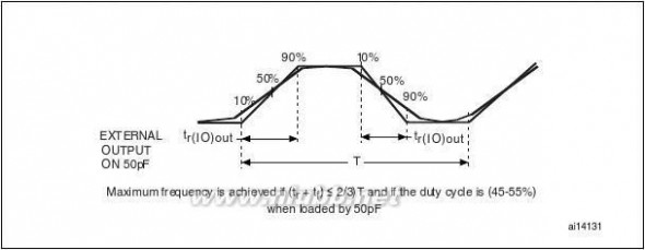
205 STM32F205xx207xx参考手册
STM32F205xx, STM32F207xx
Electrical characteristics
2.The reset network protects the device against parasitic resets.
3.The user must ensure that the level on the NRST pin can go below the VIL(NRST) max level specified in
Table43. Otherwise the reset is not taken into account by the device.
5.3.16 TIM timer characteristics
The parameters given in Table44 and Table45 are guaranteed by design.
Refer to Section5.3.14: I/O port characteristics for details on the input/output alternate
function characteristics (output compare, input capture, external clock, PWM output).Table 44.
Symboltres(TIM)
Characteristics of TIMx connected to the APB1 domain(1)
Parameter
Timer resolution timeTimer external clock
frequency on CH1 to CH4Timer resolution
= 60 MHz f
16-bit counter clock period TIMxCLK1when internal clock is APB1= 30MHz
0.0167selected
32-bit counter clock period
when internal clock is selected
10.0167
7158278865536 × 65536
71.6
Conditions
Min116.700
fTIMxCLK/2
3616655361092Max
UnittTIMxCLK
nsMHzMHzbittTIMxCLK
μstTIMxCLK
μstTIMxCLK
s
fEXTResTIM
tCOUNTER
tMAX_COUNTMaximum possible count
1.TIMx is used as a general term to refer to the TIM2, TIM3, TIM4, TIM5, TIM6, TIM7, and TIM12 timers.
Doc ID 15818 Rev 583/147
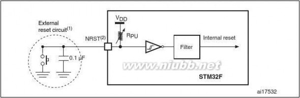
205 STM32F205xx207xx参考手册
Electrical characteristics
Table 45.
Symboltres(TIM)
STM32F205xx, STM32F207xx
Characteristics of TIMx connected to the APB2 domain(1)
Parameter
Timer resolution timeTimer external clock
frequency on CH1 to CH4Timer resolution
16-bit counter clock period when internal clock is selected
fTIMxCLK = 120MHzAPB2 = 60MHz
10.0083
Conditions
Min18.300
fTIMxCLK/2
30166553654665536 × 65536
35.79Max
UnittTIMxCLK
nsMHzMHzbittTIMxCLK
μstTIMxCLK
s
fEXTResTIMtCOUNTER
tMAX_COUNTMaximum possible count
1.TIMx is used as a general term to refer to the TIM1, TIM8, TIM9, TIM10, and TIM11 timers.
84/147Doc ID 15818 Rev 5
205 STM32F205xx207xx参考手册
STM32F205xx, STM32F207xxElectrical characteristics
5.3.17 Communications interfaces
扩展:stm32f207参考手册 / stm32f205参考手册 / stm32f207编程参考
I2C interface characteristics
Unless otherwise specified, the parameters given in Table46 are derived from tests
performed under the ambient temperature, fPCLK1 frequency and VDD supply voltage conditions summarized in Table10.
The STM32F20x and STM32F205xx I2C interface meets the requirements of the standard I2C communication protocol with the following restrictions: the I/O pins SDA and SCL are mapped to are not “true” open-drain. When configured as open-drain, the PMOS connected between the I/O pin and VDD is disabled, but is still present.
The I2C characteristics are described in Table46. Refer also to Section5.3.14: I/O port characteristics for more details on the input/output alternate function characteristics (SDA and SCL).Table 46.
Symboltw(SCLL)tw(SCLH)tsu(SDA)th(SDA)tr(SDA)tr(SCL)tf(SDA)tf(SCL)th(STA)tsu(STA)tsu(STO)tw(STO:STA)
Cb
I2C characteristics
Standard mode I2C(1)
Parameter
Min
SCL clock low timeSCL clock high timeSDA setup timeSDA data hold timeSDA and SCL rise timeSDA and SCL fall timeStart condition hold timeRepeated Start condition setup time
Stop condition setup timeStop to Start condition time (bus free)
Capacitive load for each bus line
4.04.74.04.7
400
4.74.02500(3)
1000300
0.60.6 0.6 1.3
400
μsμsμspF
Max
Min1.3 0.6 100 0(4)20 + 0.1Cb
900(3)300300
ns
Max
μs
Fast mode I2C(1)(2)
Unit
1.Guaranteed by design, not tested in production.
2.fPCLK1 must be higher than 2 MHz to achieve the maximum standard mode I2C frequency. It must be
higher than 4 MHz to achieve the maximum fast mode I2C frequency.3.The maximum hold time of the Start condition has only to be met if the interface does not stretch the low
period of SCL signal.4.The device must internally provide a hold time of at least 300ns for the SDA signal in order to bridge the
undefined region of the falling edge of SCL.
Doc ID 15818 Rev 585/147
205 STM32F205xx207xx参考手册
Electrical characteristicsSTM32F205xx, STM32F207xx
21.Measurement points are done at CMOS levels: 0.3VDD and 0.7VDD.
Table 47.
SCL frequency (fPCLK1= 30 MHz.,VDD = 3.3 V)(1)(2)
I2C_CCR value
fSCL (kHz)4003002001005020
RP = 4.7 kΩ0x80190x80210x80320x00960x012C0x02EE
1.RP = External pull-up resistance, fSCL = I2C speed,
2.For speeds around 200 kHz, the tolerance on the achieved speed is of ±5%. For other speed ranges, the
tolerance on the achieved speed ±2%. These variations depend on the accuracy of the external components used to design the application.
86/147Doc ID 15818 Rev 5
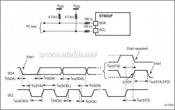
205 STM32F205xx207xx参考手册
STM32F205xx, STM32F207xxElectrical characteristics
I2S - SPI interface characteristics
Unless otherwise specified, the parameters given in Table48 for SPI or in Table49 for I2S are derived from tests performed under the ambient temperature, fPCLKx frequency and VDD supply voltage conditions summarized in Table10.
Refer to Section5.3.14: I/O port characteristics for more details on the input/output alternate function characteristics (NSS, SCK, MOSI, MISO for SPI and WS, CK, SD for I2S).Table 48.
SymbolfSCK1/tc(SCK)tr(SCK)tf(SCK)DuCy(SCK)tsu(NSS)(2)th(NSS)(2)tw(SCKH)(2)tw(SCKL)(2)tsu(MI) (2) tsu(SI)(2)th(MI) (2) th(SI)(2)ta(SO)(2)(3)tdis(SO)(2)(4)tv(SO) (2)(1)tv(MO)(2)(1)th(SO)(2)th(MO)(2)
SPI characteristics(1)
ParameterSPI clock frequency
Conditions
Master modeSlave mode
Min
Max30 30 8
304 tPCLK2 tPCLK 505554 02
3 tPCLK1025 5
152
ns
6070
UnitMHzns%
SPI clock rise and fall
Capacitive load: C = 30 pF
time
SPI slave input clock duty cycleNSS setup time NSS hold timeSCK high and low timeData input setup time
Slave modeSlave modeSlave mode
Master mode, fPCLK = 36 MHz, presc = 4Master modeSlave modeMaster modeSlave mode
Slave mode, fPCLK = 20 MHzSlave mode
Slave mode (after enable edge)Master mode (after enable edge)Slave mode (after enable edge)Master mode (after enable edge)
Data input hold timeData output access time
Data output disable time
Data output valid timeData output valid timeData output hold time
1.Remapped SPI1 characteristics to be determined.2.Based on characterization, not tested in production.
3.Min time is for the minimum time to drive the output and the max time is for the maximum time to validate
the data.4.Min time is for the minimum time to invalidate the output and the max time is for the maximum time to put
the data in Hi-Z
Doc ID 15818 Rev 587/147
205 STM32F205xx207xx参考手册
Electrical characteristics
扩展:stm32f207参考手册 / stm32f205参考手册 / stm32f207编程参考
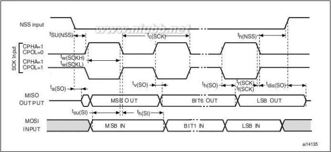
STM32F205xx, STM32F207xx
(1)
1.Measurement points are done at CMOS levels: 0.3VDD and 0.7VDD.
88/147Doc ID 15818 Rev 5
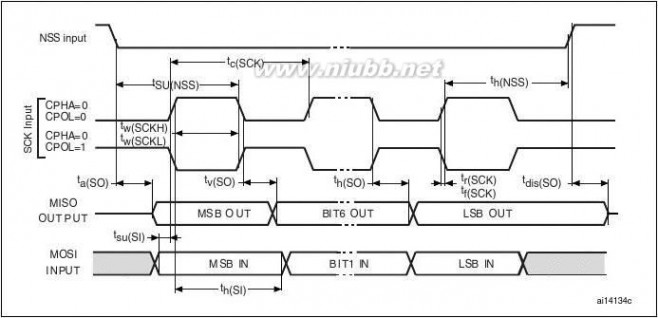
205 STM32F205xx207xx参考手册
STM32F205xx, STM32F207xx(1)
Electrical characteristics
1.Measurement points are done at CMOS levels: 0.3VDD and 0.7VDD.
Doc ID 15818 Rev 589/147

205 STM32F205xx207xx参考手册
Electrical characteristics
Table 49.
SymbolfCK
1/tc(CK)tr(CK)tf(CK)tv(WS) (2)th(WS) (2)tsu(WS) (2)th(WS) (2)tw(CKH) (2)tw(CKL) (2)tsu(SD_MR) (2)tsu(SD_SR) (2)th(SD_MR)(2)(3)th(SD_SR) (2)(3)th(SD_MR) (2)th(SD_SR) (2)tv(SD_ST) (2)(3)
STM32F205xx, STM32F207xx
I2S characteristics(1)
Parameter
I2S clock frequencyI2S clock rise and fall timeWS valid time WS hold timeWS setup time WS hold timeCK high and low timeData input setup timeData input hold timeData input hold time
ConditionsMasterSlave
capacitive load CL=50 pFMasterMasterSlaveSlave
Master fPCLK= TBD, presc = TBDMaster receiverSlave receiverMaster receiverSlave receiverMaster fPCLK = TBDSlave fPCLK = TBDSlave transmitter (after enable edge) fPCLK = TBD
TBDTBDTBDTBD TBD TBDTBD TBDTBD TBDTBD
TBD TBD
TBD
TBD
TBD TBD
TBD
Min TBD0
Max TBD TBD TBD
UnitMHz
ns
Data output valid time
th(SD_ST) (2)
Data output hold time
Slave transmitter (after enable edge)Master transmitter (after enable edge)fPCLK = TBD
tv(SD_MT) (2)(3)
Data output valid time
th(SD_MT) (2)
Data output hold time
Master transmitter (after enable edge)
1.TBD = to be determined.
2.Based on design simulation and/or characterization results, not tested in production.3.Depends on fPCLK. For example, if fPCLK=8 MHz, then TPCLK = 1/fPLCLK =125 ns.
90/147Doc ID 15818 Rev 5
205 STM32F205xx207xx参考手册
STM32F205xx, STM32F207xx
2(1)
Electrical characteristics
1.Measurement points are done at CMOS levels: 0.3 × VDD and 0.7 × VDD.
2.LSB transmit/receive of the previously transmitted byte. No LSB transmit/receive is sent before the first
byte.

2(1)
1.Based on characterization, not tested in production.
2.LSB transmit/receive of the previously transmitted byte. No LSB transmit/receive is sent before the first
byte.
Doc ID 15818 Rev 591/147
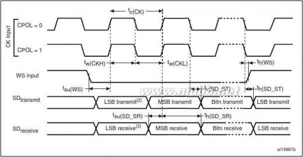
205 STM32F205xx207xx参考手册
Electrical characteristicsSTM32F205xx, STM32F207xx
USB OTG FS characteristics
The USB OTG interface is USB-IF certified (Full-Speed). This interface is present in both the USB OTG HS and USB OTG FS controllers.Table 50.
tSTARTUP(1)
USB OTG FS startup time
Parameter
USB OTG FS transceiver startup time
Max1
Unitμs
Symbol
1.Guaranteed by design, not tested in production.
Table 51.
Symbol
USB OTG FS DC electrical characteristics
Parameter
USB OTG FS operating voltage
I(USB_FS_DP/DM, USB_HS_DP/DM) Includes VDI range
Conditions
Min.(1)Typ.Max.(1)Unit3.0(2)0.20.81.3
RL of 1.5kΩ to 3.6V(4)RL of 15
kΩ to VSS(4)
2.817
VIN = VDD
0.65
1.1
2.0
kΩ
VIN = VSSVIN = VSS
1.5
1.8
2.1
21
2.52.00.33.624
VV
3.6
V
VDD
Input levels
VDI(3)Differential input sensitivityVCM(3)VSE(3)
Differential common mode range
Single ended receiver threshold
Static output level lowStatic output level highPA11, PA12, PB14, PB15 (USB_FS_DP/DM, USB_HS_DP/DM) PA9, PB13
(OTG_FS_VBUS, OTG_HS_VBUS)
PA12, PB15 (USB_FS_DP, USB_HS_DP)
Output levels
VOLVOH
RPD
RPU
PA9, PB13
(OTG_FS_VBUS, OTG_HS_VBUS)
0.250.370.55
1.All the voltages are measured from the local ground potential.
2.The STM32F20x and STM32F205xx USB OTG FS functionality is ensured down to 2.7 V but not the full
USB OTG FS electrical characteristics which are degraded in the 2.7-to-3.0 V VDD voltage range.3.Guaranteed by design, not tested in production.4.RL is the load connected on the USB OTG FS drivers
92/147Doc ID 15818 Rev 5
205 STM32F205xx207xx参考手册
STM32F205xx, STM32F207xxElectrical characteristics
Doc ID 15818 Rev 593/147
扩展:stm32f207参考手册 / stm32f205参考手册 / stm32f207编程参考
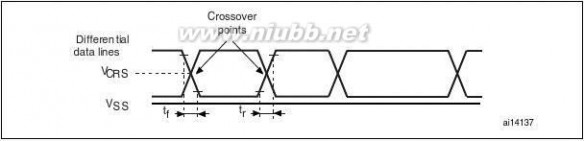
205 STM32F205xx207xx参考手册
Electrical characteristics
Table 52.
STM32F205xx, STM32F207xx
USB OTG FS electrical characteristics(1)
Driver characteristics
Symbol
trtftrfmVCRS
Parameter
Rise time(2)Fall timeRise/ fall time matchingOutput signal crossover voltage
ConditionsCL = 50 pF CL = 50 pF
tr/tf
Min44901.3
Max20201102.0
Unitnsns%V
1.Guaranteed by design, not tested in production.
2.Measured from 10% to 90% of the data signal. For more detailed informations, please refer to USB
Specification - Chapter 7 (version 2.0).
USB HS characteristics
Table 53.
Clock timing parameters
Parameter(1)
Symbol
8-bit ±10%
FSTART_8BITFSTEADYDSTART_8BITDSTEADY
Min5459.974049.975
Nominal60605050
Max6660.036050.0251.45.6
UnitMHzMHz%%msmsμspsns
Frequency (first transition)
Frequency (steady state) ±500ppmDuty cycle (first transition)
8-bit ±10%
Duty cycle (steady state) ±500ppm
Time to reach the steady state frequency and
TSTEADY
duty cycle after the first transitionClock startup time after the de-assertion of SuspendM
PeripheralHost
TSTART_DEVTSTART_HOST
PHY preparation time after the first transition
TPREP
of the input clockJitterRise timeFall time
1.Guaranteed by design, not tested in production.
TJITTERTRISETFALL
94/147Doc ID 15818 Rev 5
205 STM32F205xx207xx参考手册
STM32F205xx, STM32F207xx
Electrical characteristics
Table 54.
ULPI timing
Value(1)
Parameter
Setup time (control in)
Symbol
Min.
tSC, tSDtHC, tHDtDC, tDDtSC, tSDtHC, tHDtDC, tDD
1.5
6.0
0.0
9.03.0Max.6.0
nsnsnsnsnsnsUnit
Output clockHold time (control in)Output delay (control out)Setup time (control in)
Input clock (optional)
Hold time (control in)Output delay (control out)
1.VDD = 3V to 3.6V and TA = –40 to 85°C.
Ethernet characteristics
Table55 shows the Ethernet operating voltage.Table 55.
Ethernet DC electrical characteristics
Parameter
VDD
Ethernet operating voltage
Min.(1)3.0
Max.(1)3.6
UnitV
Symbol
Input level
1.All the voltages are measured from the local ground potential.
Table56 gives the list of Ethernet MAC signals for the SMI (station management interface) and Figure37 shows the corresponding timing diagram.
Doc ID 15818 Rev 595/147
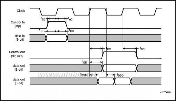
205 STM32F205xx207xx参考手册
Electrical characteristics
STM32F205xx, STM32F207xx
Table 56.
SymboltMDCtd(MDIO)th(MDIO)
Dynamics characteristics: Ethernet MAC signals for SMI(1)
Rating
MDC cycle time (1.71MHz, AHB = 72MHz)MDIO write data valid time
MinTBDTBDTBDTBD
TypTBDTBDTBDTBD
MaxTBDTBDTBDTBD
Unitnsnsnsns
tsu(MDIO)Read data setup time
Read data hold time
1.TBD stands for to be determined.
Table57 gives the list of Ethernet MAC signals for the RMII and Figure38 shows the corresponding timing diagram.
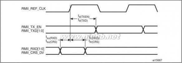
Table 57.
Symboltsu(RXD)tih(RXD)tsu(CRS)tih(CRS)td(TXEN)td(TXD)
Dynamics characteristics: Ethernet MAC signals for RMII(1)
Rating
Receive data setup timeReceive data hold timeCarrier sense set-up timeCarrier sense hold timeTransmit enable valid delay timeTransmit data valid delay time
MinTBDTBDTBDTBD00
TypTBDTBDTBDTBD9.69.9
MaxTBDTBDTBDTBD21.921
Unitnsnsnsnsnsns
1.TBD stands for to be determined.
96/147Doc ID 15818 Rev 5
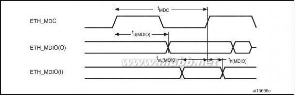
205 STM32F205xx207xx参考手册
STM32F205xx, STM32F207xxElectrical characteristics
Table58 gives the list of Ethernet MAC signals for MII and Figure38 shows the corresponding timing diagram.
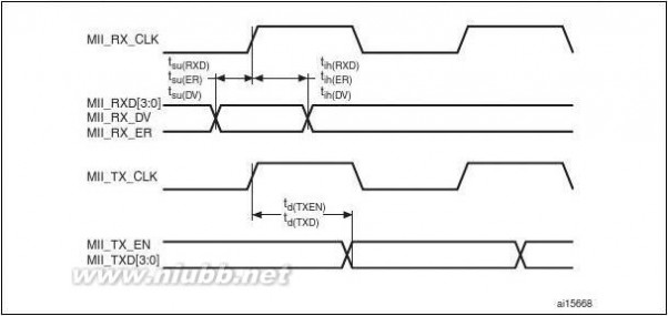
Table 58.
Symboltsu(RXD)tih(RXD)tsu(DV)tih(DV)tsu(ER)tih(ER)td(TXEN)td(TXD)
Dynamics characteristics: Ethernet MAC signals for MII(1)
Rating
Receive data setup timeReceive data hold timeData valid setup timeData valid hold timeError setup timeError hold time
Transmit enable valid delay timeTransmit data valid delay time
MinTBDTBDTBDTBDTBDTBD13.412.9
TypTBDTBDTBDTBDTBDTBD15.516.1
MaxTBDTBDTBDTBDTBDTBD17.719.4
Unitnsnsnsnsnsnsnsns
扩展:stm32f207参考手册 / stm32f205参考手册 / stm32f207编程参考
1.TBD stands for to be determined.
CAN (controller area network) interface
Refer to Section5.3.14: I/O port characteristics for more details on the input/output alternate function characteristics (CANTX and CANRX).
Doc ID 15818 Rev 597/147
205 STM32F205xx207xx参考手册
Electrical characteristicsSTM32F205xx, STM32F207xx
5.3.18 12-bit ADC characteristics
Unless otherwise specified, the parameters given in Table59 are derived from tests
performed under the ambient temperature, fPCLK2 frequency and VDDA supply voltage conditions summarized in Table10.
Table 59.
SymbolVDDAVREF+IVREFfADCfTRIG(1)VAINRAIN(1)RADC(1)CADC(1)tlat(1)tlatr(1)tS(1)tSTAB(1)
ADC characteristics
Parameter
Power supply
Positive reference voltageCurrent on the VREF input pinADC clock frequency
VDDA = 1.8 to 2.4VVDDA = 2.4 to 3.6VfADC = 30 MHz
0 (VSSA or VREF- tied to ground)
See Equation 1 for
details
0.60.6
Conditions
Min1.81.65
160(1)Typ
Max3.6VDDA220(1)153082317VREF+501
fADC = 30MHzfADC = 30MHzfADC = 30MHz
0.10030
fADC = 30MHz12-bit resolutionfADC = 30MHz10-bit resolution
0.50.430.370.3
80.1003(3)0.0672(3)16480116.4016.3416.2716.20
UnitVVμAMHzMHzkHz1/fADCVkΩkΩpFμs1/fADCμs1/fADCμs1/fADCμsμsμsμsμs1/fADC
External trigger frequencyConversion voltage range(2)External input impedanceSampling switch resistanceInternal sample and hold capacitor
Injection trigger conversion latency
Regular trigger conversion latency
Sampling time Power-up time
tCONV(1)
Total conversion time (including sampling time)
fADC = 30MHz8-bit resolutionfADC = 30MHz6-bit resolution
9 to 492 (tS for sampling +n-bit resolution for successive approximation)
98/147Doc ID 15818 Rev 5
205 STM32F205xx207xx参考手册
STM32F205xx, STM32F207xxTable 59.
Symbol
Electrical characteristics
ADC characteristics (continued)
Parameter
Conditions12-bit resolutionSingle ADC
Min
Typ
Max2
UnitMsps
fS(1)
Sampling rate (fADC = 30 MHz)
12-bit resolutionInterleave Dual ADC
mode12-bit resolutionInterleave Triple ADC
modefADC = 30 MHz3 sampling time12-bit resolutionfADC = 30 MHz480 sampling time12-bit resolutionfADC = 30 MHz3 sampling time12-bit resolutionfADC = 30 MHz480 sampling time12-bit resolution
4Msps
6Msps
TBDμA
IVREF+
ADC VREF DC current
consumption in conversion mode
TBDμA
TBDμA
IDDA
ADC VDDA DC current
consumption in conversion mode
TBDμA
1.Based on characterization, not tested in production.
2.VREF+ is internally connected to VDDA and VREF- is internally connected to VSSA.
3.For external triggers, a delay of 1/fPCLK2 must be added to the latency specified in Table59.
Equation 1: RAIN max formula
The formula above (Equation 1) is used to determine the maximum external impedance allowed for anerror below 1/4 of LSB. Here N = 12 (from 12-bit resolution).
Table 60.
SymbolETEOEGEDEL
a
ADC accuracy (1)
Parameter
Total unadjusted errorOffset errorGain error
Differential linearity errorIntegral linearity error
fPCLK2 = 60 MHz,
fADC = 30 MHz, RAIN < 10 kΩ, VDDA = 1.8 V to 3.6 V
Test conditions
Typ±2±1.5±1.5±1±1.5
Max(2)±5±2.5±3±2±3
LSBUnit
1.Better performance could be achieved in restricted VDD, frequency and temperature ranges.2.Based on characterization, not tested in production.
Note:
ADC accuracy vs. negative injection current: Injecting a negative current on any of the
standard (non-robust) analog input pins should be avoided as this significantly reduces the accuracy of the conversion being performed on another analog input. It is recommended to
Doc ID 15818 Rev 599/147
205 STM32F205xx207xx参考手册
Electrical characteristicsSTM32F205xx, STM32F207xx
add a Schottky diode (pin to ground) to standard analog pins which may potentially inject negative currents.
Any positive injection current within the limits specified for IINJ(PIN) and ΣIINJ(PIN) in Section5.3.14 does not affect the ADC accuracy.

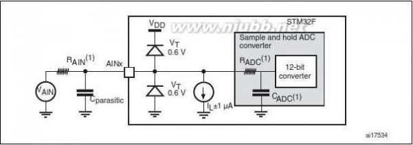
1.Refer to Table59 for the values of RAIN, RADC and CADC.
2.Cparasitic represents the capacitance of the PCB (dependent on soldering and PCB layout quality) plus the
pad capacitance (roughly 7pF). A high Cparasitic value downgrades conversion accuracy. To remedy this, fADC should be reduced.
100/147Doc ID 15818 Rev 5
205 STM32F205xx207xx参考手册 扩展:stm32f207参考手册 / stm32f205参考手册 / stm32f207编程参考
STM32F205xx, STM32F207xxElectrical characteristics
General PCB design guidelines
Power supply decoupling should be performed as shown in Figure42 or Figure43,
depending on whether VREF+ is connected to VDDA or not. The 10 nF capacitors should be
ceramic (good quality). They should be placed them as close as possible to the chip.
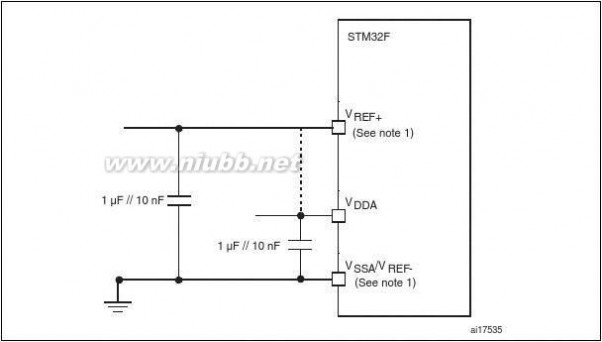
1.VREF+ and VREF– inputs are available only on 100-pin packages.
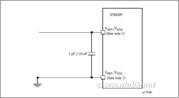
1.VREF+ and VREF– inputs are available only on 100-pin packages.
Doc ID 15818 Rev 5101/147
205 STM32F205xx207xx参考手册
Electrical characteristicsSTM32F205xx, STM32F207xx
5.3.19 DAC electrical specifications
Table 61.
SymbolVDDAVREF+VSSARLOAD(1)RO(1)
DAC characteristics
Parameter
Analog supply voltageReference supply voltageGround
Resistive load with buffer ONImpedance output with buffer
OFF
Min1.81.805
Typ
Max3.6 3.60
UnitVVVkΩ
When the buffer is OFF, the
Minimum resistive load between DAC_OUT and VSS to have a 1% accuracy is 1.5MΩ
Maximum capacitive load at
DAC_OUT pin (when the buffer is ON).
It gives the maximum output excursion of the DAC.
It corresponds to 12-bit input code (0x0E0) to (0xF1C) at VREF+ = 3.6V and (0x1C7) to (0xE38) at VREF+ = 1.8V
It gives the maximum output excursion of the DAC.
With no load, worst code (0xF1C) at VREF+ = 3.6V in terms of DC consumption on the inputsWith no load, middle code (0x800) on the inputs
With no load, worst code (0xF1C) at VREF+ = 3.6V in terms of DC consumption on the inputsGiven for the DAC in 10-bit configuration.
Given for the DAC in 12-bit configuration.
Given for the DAC in 10-bit configuration.
Given for the DAC in 12-bit configuration.VREF+ ≤ VDDA
Comments
15kΩ
CLOAD(1)
Capacitive load50pF
DAC_OUT Lower DAC_OUT voltage min(1)with buffer ONDAC_OUT Higher DAC_OUT voltage
with buffer ONmax(1)
DAC_OUT Lower DAC_OUT voltage
min(1)with buffer OFFDAC_OUT Higher DAC_OUT voltage
with buffer OFFmax(1)IVREF+
DAC DC VREF current consumption in quiescent mode (Standby mode)DAC DC VDDA current consumption in quiescent mode (Standby mode)
VDDA – 0.2
0.5
VREF+ – 1LSB
220
VmVV
μA
380μA
IDDA
480μA
DNL(2)
Differential non linearity Difference between two consecutive code-1LSB)Integral non linearity (difference between
measured value at Code i and the value at Code i on a line drawn between Code 0 and last Code 1023)
±1
LSB
INL(2)
±4LSB
102/147Doc ID 15818 Rev 5
205 STM32F205xx207xx参考手册
STM32F205xx, STM32F207xxTable 61.
Symbol
Electrical characteristics
DAC characteristics (continued)
Parameter
Offset error
(difference between
measured value at Code (0x800) and the ideal value = VREF+/2)Gain error
Min
Typ
Max±10±3±12±0.5
UnitmVLSBLSB%
Comments
Given for the DAC in 12-bit configuration
Given for the DAC in 10-bit at VREF+ = 3.6V
Given for the DAC in 12-bit at VREF+ = 3.6V
Given for the DAC in 12bit configuration
Offset(2)
Gain error(2)
Settling time (full scale: for a 10-bit input code transition between the lowest and the
tSETTLING(2)
highest input codes when DAC_OUT reaches final value ±4LSBTHD(2)
Total Harmonic DistortionBuffer ON
Max frequency for a correct DAC_OUT change when small variation in the input code (from code i to i+1LSB)Wakeup time from off state (Setting the ENx bit in the DAC Control register)Power supply rejection ratio (to VDDA) (static DC measurement)
34μs
pF,CLOAD ≤ 50
RLOAD ≥ 5 kΩ
dB
pF,CLOAD ≤ 50
RLOAD ≥ 5 kΩpF,CLOAD ≤ 50
RLOAD ≥ 5 kΩ
pF, RLOAD ≥ 5 kΩCLOAD ≤ 50
input code between lowest and highest possible ones.No RLOAD, CLOAD = 50 pF
Update
rate(1)
1MS/s
tWAKEUP(2)
6.510μs
PSRR+
(1)
dB
1.Guaranteed by design, not tested in production.
2.Guaranteed by characterization, not tested in production.
1.The DAC integrates an output buffer that can be used to reduce the output impedance and to drive external loads directly
without the use of an external operational amplifier. The buffer can be bypassed by configuring the BOFFx bit in the DAC_CR register.
Doc ID 15818 Rev 5103/147

205 STM32F205xx207xx参考手册
Electrical characteristicsSTM32F205xx, STM32F207xx
扩展:stm32f207参考手册 / stm32f205参考手册 / stm32f207编程参考
5.3.20 Temperature sensor characteristics
Table 62.
SymbolTL(1)V25(1)tSTART(2)TS_temp
(3)(2)
TS characteristics
Parameter
VSENSE linearity with temperature
Min
Typ±12.50.76
416
10Max±2
Unit°CmV/°CVμsμs
Avg_Slope(1)Average slope
Voltage at 25 °CStartup time
ADC sampling time when reading the
temperature1°C accuracy
1.Based on characterization, not tested in production.2.Guaranteed by design, not tested in production.
3.Shortest sampling time can be determined in the application by multiple iterations.
5.3.21 VBAT monitoring characteristics
Table 63.
SymbolR(1)
VBAT monitoring characteristics
Parameter
Resistor bridge for VBATRatio on VBAT measurementError on Q
ADC sampling time when reading the VBAT1mV accuracy
-1TBDMin
TypTBD2
+1
%μs
Max
UnitKOhm
Q(1)
Er(1)TS_vbat(2)(2)
1.Guaranteed by design, not tested in production.
2.Shortest sampling time can be determined in the application by multiple iterations.
5.3.22 Embedded reference voltage
The parameters given in Table64 are derived from tests performed under ambient
temperature and VDD supply voltage conditions summarized in Table10.Table 64.
SymbolVREFINT
Embedded internal reference voltage
Parameter
Internal reference voltageADC sampling time when reading the internal reference voltage
Conditions–40 °C < TA < +105°C–40 °C < TA < +85°C
Min1.161.16
Typ 1.201.205.1
Max1.261.24TBD(2)
UnitVVμs
TS_vrefint
(1)
104/147Doc ID 15818 Rev 5
205 STM32F205xx207xx参考手册
STM32F205xx, STM32F207xx
Table 64.
SymbolVRERINT(2)TCoeff(2)
Electrical characteristics
Embedded internal reference voltage
Parameter
Internal reference voltage spread over the temperature range
Temperature coefficient
ConditionsVDD = 3 V ±10 mV
Min
Typ
Max10100
UnitmVppm/°C
1.Shortest sampling time can be determined in the application by multiple iterations.2.Guaranteed by design, not tested in production.
5.3.23 FSMC characteristics
Asynchronous waveforms and timings
Figure45 through Figure48 represent asynchronous waveforms and Table65 through
Table68 provide the corresponding timings. The results shown in these tables are obtained with the following FSMC configuration:
●●●
AddressSetupTime = 0AddressHoldTime = 1DataSetupTime = 1
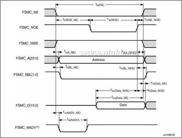
1.Mode 2/B, C and D only. In Mode 1, FSMC_NADV is not used.
Doc ID 15818 Rev 5105/147
205 STM32F205xx207xx参考手册
Electrical characteristics
Table 65.
Symboltw(NE)tv(NOE_NE)tw(NOE)th(NE_NOE)tv(A_NE)th(A_NOE)tv(BL_NE)th(BL_NOE)tsu(Data_NE)th(Data_NOE)th(Data_NE)tv(NADV_NE)tw(NADV)
1.CL = 15 pF.
2.Based on characterization, not tested in production.
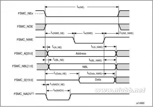
STM32F205xx, STM32F207xx
Asynchronous non-multiplexed SRAM/PSRAM/NOR read timings(1) (2)
Parameter
FSMC_NE low time
FSMC_NEx low to FSMC_NOE lowFSMC_NOE low time
Min5THCLK – 1.50.5
5THCLK – 1.5
Max5THCLK + 21.5
5THCLK + 1.57
0.1
2THCLK + 252THCLK + 2500
5
THCLK + 1.5
Unitnsnsnsnsnsnsnsnsnsnsnsnsnsns
FSMC_NOE high to FSMC_NE high hold time–1.5FSMC_NEx low to FSMC_A validAddress hold time after FSMC_NOE highFSMC_NEx low to FSMC_BL validFSMC_BL hold time after FSMC_NOE highData to FSMC_NEx high setup time
tsu(Data_NOE)Data to FSMC_NOEx high setup time
Data hold time after FSMC_NOE highData hold time after FSMC_NEx highFSMC_NEx low to FSMC_NADV lowFSMC_NADV low time
1.Mode 2/B, C and D only. In Mode 1, FSMC_NADV is not used.
106/147Doc ID 15818 Rev 5
205 STM32F205xx207xx参考手册
STM32F205xx, STM32F207xx
Table 66.
Symboltw(NE)tv(NWE_NE)tw(NWE)th(NE_NWE)tv(A_NE)th(A_NWE)tv(BL_NE)th(BL_NWE)tv(Data_NE)th(Data_NWE)tv(NADV_NE)tw(NADV)
1.CL = 15 pF.
2.Based on characterization, not tested in production.
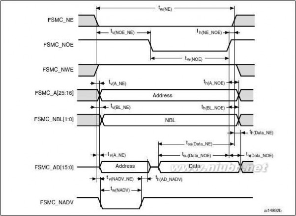
Electrical characteristics
Asynchronous non-multiplexed SRAM/PSRAM/NOR write timings(1)(2)
Parameter
FSMC_NE low time
FSMC_NEx low to FSMC_NWE lowFSMC_NWE low time
FSMC_NWE high to FSMC_NE high hold timeFSMC_NEx low to FSMC_A validAddress hold time after FSMC_NWE highFSMC_NEx low to FSMC_BL valid
FSMC_BL hold time after FSMC_NWE highFSMC_NEx low to Data valid
Data hold time after FSMC_NWE highFSMC_NEx low to FSMC_NADV lowFSMC_NADV low time
扩展:stm32f207参考手册 / stm32f205参考手册 / stm32f207编程参考
THCLK
5.5THCLK + 1.5
THCLK – 0.5
THCLK + 7
THCLK
1.5
Min3THCLK – 1THCLK – 0.5THCLK – 0.5THCLK
7.5
Max3THCLK + 2THCLK + 1.5THCLK + 1.5
Unitnsnsnsnsnsnsnsnsnsnsnsns
Doc ID 15818 Rev 5107/147
205 STM32F205xx207xx参考手册
Electrical characteristics
Table 67.
Symboltw(NE)tv(NOE_NE)tw(NOE)th(NE_NOE)tv(A_NE)tv(NADV_NE)tw(NADV)th(AD_NADV)th(A_NOE)th(BL_NOE)tv(BL_NE)tsu(Data_NE)th(Data_NE)th(Data_NOE)
1.CL = 15 pF.
2.Based on characterization, not tested in production.
STM32F205xx, STM32F207xx
Asynchronous multiplexed PSRAM/NOR read timings(1)(2)
Parameter
FSMC_NE low time
FSMC_NEx low to FSMC_NOE lowFSMC_NOE low time
FSMC_NOE high to FSMC_NE high hold timeFSMC_NEx low to FSMC_A validFSMC_NEx low to FSMC_NADV lowFSMC_NADV low time
FSMC_AD (address) valid hold time after FSMC_NADV high
Address hold time after FSMC_NOE highFSMC_BL hold time after FSMC_NOE highFSMC_NEx low to FSMC_BL validData to FSMC_NEx high setup timeData hold time after FSMC_NEx highData hold time after FSMC_NOE high
2THCLK + 242THCLK + 25003
THCLK –1.5THCLKTHCLK0
Min7THCLK – 24THCLK – 1–1
05
THCLK + 1.5
Max7THCLK + 24THCLK + 2
Unit ns ns ns ns ns ns ns ns ns ns ns ns ns ns
3THCLK – 0.53THCLK + 1.5 ns
tsu(Data_NOE)Data to FSMC_NOE high setup time
108/147Doc ID 15818 Rev 5
205 STM32F205xx207xx参考手册
STM32F205xx, STM32F207xxElectrical characteristics
Table 68.
Symboltw(NE)tv(NWE_NE)tw(NWE)th(NE_NWE)tv(A_NE)tv(NADV_NE)tw(NADV)th(AD_NADV)th(A_NWE)tv(BL_NE)th(BL_NWE)
Asynchronous multiplexed PSRAM/NOR write timings(1)(2)
Parameter
FSMC_NE low time
FSMC_NEx low to FSMC_NWE lowFSMC_NWE low time
FSMC_NWE high to FSMC_NE high hold timeFSMC_NEx low to FSMC_A validFSMC_NEx low to FSMC_NADV lowFSMC_NADV low time
FSMC_AD (address) valid hold time after FSMC_NADV high
Address hold time after FSMC_NWE highFSMC_NEx low to FSMC_BL valid
FSMC_BL hold time after FSMC_NWE high
THCLK – 1.5
THCLK + 1.5
THCLK – 53THCLK – 1THCLK – 34THCLK
1.6
Min5THCLK – 12THCLK2THCLK – 1THCLK – 1
75THCLK + 1
Max5THCLK + 22THCLK + 12THCLK + 2
Unitnsnsnsnsnsnsnsnsnsnsnsnsns
tv(Data_NADV)FSMC_NADV high to Data validth(Data_NWE)
1.CL = 15 pF.
2.Based on characterization, not tested in production.
Data hold time after FSMC_NWE high
Doc ID 15818 Rev 5109/147
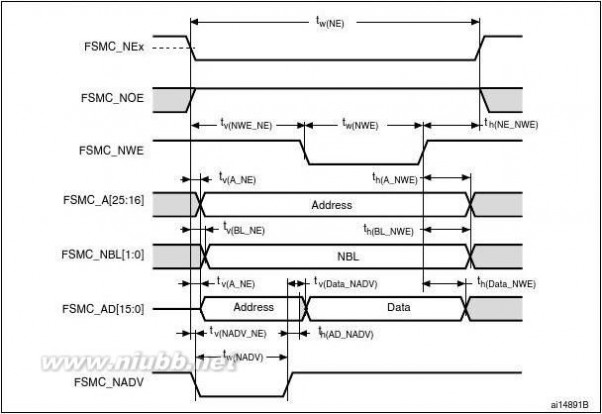
205 STM32F205xx207xx参考手册
Electrical characteristicsSTM32F205xx, STM32F207xx
Synchronous waveforms and timings
Figure49 through Figure52 represent synchronous waveforms and Table70 through
Table72 provide the corresponding timings. The results shown in these tables are obtained with the following FSMC configuration:
●●●●●
BurstAccessMode = FSMC_BurstAccessMode_Enable;MemoryType = FSMC_MemoryType_CRAM;WriteBurst = FSMC_WriteBurst_Enable;
CLKDivision = 1; (0 is not supported, see the STM32F20xxx/21xxx reference manual)DataLatency = 1 for NOR Flash; DataLatency = 0 for PSRAM
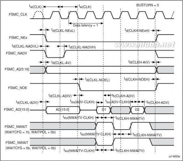
110/147Doc ID 15818 Rev 5
205 STM32F205xx207xx参考手册
STM32F205xx, STM32F207xx
Table 69.
Symboltw(CLK)td(CLKL-NExL)td(CLKH-NExH)td(CLKL-NADVL)td(CLKL-NADVH)td(CLKL-AV)td(CLKH-AIV)td(CLKL-NOEL)td(CLKH-NOEH)td(CLKL-ADV)td(CLKL-ADIV)tsu(ADV-CLKH)th(CLKH-ADV)
FSMC_CLK period
FSMC_CLK low to FSMC_NEx low (x = 0...2)FSMC_CLK high to FSMC_NEx high (x = 0...2)FSMC_CLK low to FSMC_NADV lowFSMC_CLK low to FSMC_NADV high
FSMC_CLK low to FSMC_Ax valid (x = 16...25)
5
Electrical characteristics
Synchronous multiplexed NOR/PSRAM read timings(1)(2)
Parameter
Min27.7
1.5
THCLK + 2
4Max
Unit ns ns ns ns ns
ns ns
THCLK +1
THCLK + 0.5
12
ns ns ns ns
FSMC_CLK high to FSMC_Ax invalid (x = 16...25)THCLK + 2FSMC_CLK low to FSMC_NOE lowFSMC_CLK high to FSMC_NOE highFSMC_CLK low to FSMC_AD[15:0] validFSMC_CLK low to FSMC_AD[15:0] invalidFSMC_A/D[15:0] valid data before FSMC_CLK high
6ns
ns ns ns
FSMC_A/D[15:0] valid data after FSMC_CLK highTHCLK – 10
82
tsu(NWAITV-CLKH)FSMC_NWAIT valid before FSMC_CLK highth(CLKH-NWAITV)
1.CL = 15 pF.
2.Based on characterization, not tested in production.
FSMC_NWAIT valid after FSMC_CLK high
Doc ID 15818 Rev 5111/147
205 STM32F205xx207xx参考手册
Electrical characteristicsSTM32F205xx, STM32F207xx112/147Doc ID 15818 Rev 5

扩展:stm32f207参考手册 / stm32f205参考手册 / stm32f207编程参考
205 STM32F205xx207xx参考手册
STM32F205xx, STM32F207xx
Table 70.
Symboltw(CLK)td(CLKL-NExL)td(CLKH-NExH)td(CLKL-NADVL)td(CLKL-NADVH)td(CLKL-AV)td(CLKH-AIV)td(CLKL-NWEL)td(CLKH-NWEH)td(CLKL-ADV)td(CLKL-ADIV)td(CLKL-Data)tsu(NWAITV-CLKH)th(CLKH-NWAITV)td(CLKL-NBLH)
1.CL = 15 pF.
2.Based on characterization, not tested in production.
Electrical characteristics
Synchronous multiplexed PSRAM write timings(1)(2)
Parameter
FSMC_CLK period
FSMC_CLK low to FSMC_Nex low (x = 0...2)FSMC_CLK high to FSMC_NEx high (x = 0...2)FSMC_CLK low to FSMC_NADV lowFSMC_CLK low to FSMC_NADV high
FSMC_CLK low to FSMC_Ax valid (x = 16...25)FSMC_CLK high to FSMC_Ax invalid (x = 16...25)FSMC_CLK low to FSMC_NWE lowFSMC_CLK high to FSMC_NWE highFSMC_CLK low to FSMC_AD[15:0] validFSMC_CLK low to FSMC_AD[15:0] invalidFSMC_A/D[15:0] valid after FSMC_CLK lowFSMC_NWAIT valid before FSMC_CLK highFSMC_NWAIT valid after FSMC_CLK highFSMC_CLK low to FSMC_NBL high
7213
6
THCLK +1
12
TCK + 2
1
5
THCLK + 2
4
Min27.7
2Max
Unit ns ns ns ns ns ns ns ns ns ns ns ns ns ns ns
Doc ID 15818 Rev 5113/147
205 STM32F205xx207xx参考手册
Electrical characteristicsSTM32F205xx, STM32F207xx
Table 71.
Symboltw(CLK)td(CLKL-NExL)td(CLKH-NExH)td(CLKL-NADVL)
Synchronous non-multiplexed NOR/PSRAM read timings(1)(2)
Parameter
FSMC_CLK period
FSMC_CLK low to FSMC_NEx low (x = 0...2)FSMC_CLK high to FSMC_NEx high (x = 0...2)FSMC_CLK low to FSMC_NADV lowFSMC_CLK low to FSMC_NADV highFSMC_CLK low to FSMC_Ax valid (x = 0...25)
FSMC_CLK high to FSMC_Ax invalid (x = 0...25)THCLK + 4FSMC_CLK low to FSMC_NOE lowFSMC_CLK high to FSMC_NOE high
THCLK + 1.57725
THCLK + 2
4
Min27.7
1.5
Max
Unit ns ns ns ns ns ns ns
THCLK + 1.5 ns
ns ns ns ns ns
td(CLKL-NADVH)td(CLKL-AV)td(CLKH-AIV)td(CLKL-NOEL)td(CLKH-NOEH)tsu(DV-CLKH)th(CLKH-DV)th(CLKH-NWAITV)
1.CL = 15 pF.
FSMC_D[15:0] valid data before FSMC_CLK high6.5FSMC_D[15:0] valid data after FSMC_CLK high
tsu(NWAITV-CLKH)FSMC_NWAIT valid before FSMC_SMCLK high
FSMC_NWAIT valid after FSMC_CLK high
2.Based on characterization, not tested in production.
114/147Doc ID 15818 Rev 5
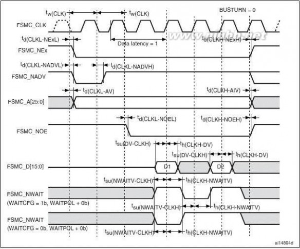
205 STM32F205xx207xx参考手册
STM32F205xx, STM32F207xxElectrical characteristics
Table 72.
Symboltw(CLK)td(CLKL-NExL)td(CLKH-NExH)
Synchronous non-multiplexed PSRAM write timings(1)(2)
Parameter
FSMC_CLK period
FSMC_CLK low to FSMC_NEx low (x = 0...2) FSMC_CLK high to FSMC_NEx high (x = 0...2) FSMC_CLK low to FSMC_NADV low FSMC_CLK low to FSMC_NADV high
FSMC_CLK low to FSMC_Ax valid (x = 16...25) FSMC_CLK high to FSMC_Ax invalid (x = 16...25) FSMC_CLK low to FSMC_NWE low FSMC_CLK high to FSMC_NWE high
FSMC_D[15:0] valid data after FSMC_CLK low
721THCLK + 1
6
TCK + 2
1
5
THCLK + 2
4
Min27.7
2Max
Unit ns ns ns ns ns ns ns ns ns ns ns ns ns
td(CLKL-NADVL)td(CLKL-NADVH)td(CLKL-AV)td(CLKH-AIV)td(CLKL-NWEL)td(CLKH-NWEH)td(CLKL-Data)th(CLKH-NWAITV)td(CLKL-NBLH)
1.CL = 15 pF.
tsu(NWAITV-CLKH) FSMC_NWAIT valid before FSMC_CLK high
FSMC_NWAIT valid after FSMC_CLK high FSMC_CLK low to FSMC_NBL high
2.Based on characterization, not tested in production.
Doc ID 15818 Rev 5115/147
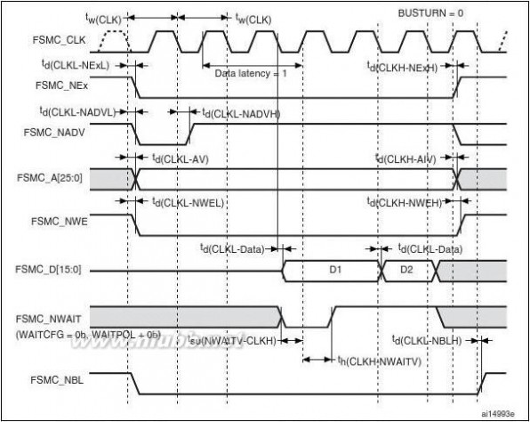
205 STM32F205xx207xx参考手册
Electrical characteristicsSTM32F205xx, STM32F207xxPC Card/CompactFlash controller waveforms and timings
Figure53 through Figure58 represent synchronous waveforms and Table73 provides the
corresponding timings. The results shown in this table are obtained with the following FSMC
configuration:
●
●
●
●
●
●
●
●
●
●
●
●
●
●COM.FSMC_SetupTime = 0x04;COM.FSMC_WaitSetupTime = 0x07;COM.FSMC_HoldSetupTime = 0x04;COM.FSMC_HiZSetupTime = 0x00;ATT.FSMC_SetupTime = 0x04;ATT.FSMC_WaitSetupTime = 0x07;ATT.FSMC_HoldSetupTime = 0x04;ATT.FSMC_HiZSetupTime = 0x00;IO.FSMC_SetupTime = 0x04;IO.FSMC_WaitSetupTime = 0x07;IO.FSMC_HoldSetupTime = 0x04;IO.FSMC_HiZSetupTime = 0x00;TCLRSetupTime = 0;TARSetupTime = 0;
Figure 53.PC Card/CompactFlash controller waveforms for common memory read
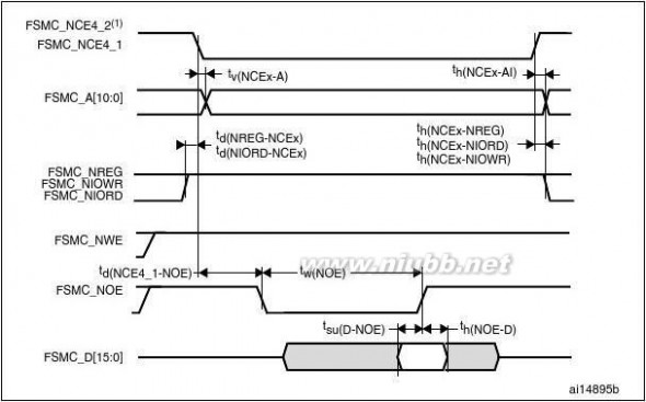
1.FSMC_NCE4_2 remains high (inactive during 8-bit access.
116/147Doc ID 15818 Rev 5
205 STM32F205xx207xx参考手册
STM32F205xx, STM32F207xxElectrical characteristics
扩展:stm32f207参考手册 / stm32f205参考手册 / stm32f207编程参考
Figure 54.PC Card/CompactFlash controller waveforms for common memory write
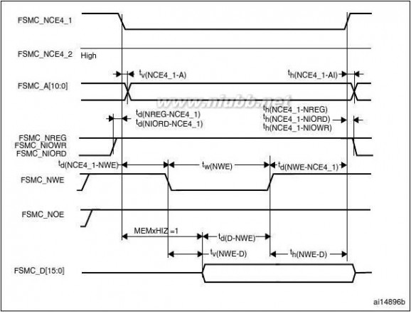
Doc ID 15818 Rev 5117/147
205 STM32F205xx207xx参考手册
Electrical characteristicsSTM32F205xx, STM32F207xxFigure 55.PC Card/CompactFlash controller waveforms for attribute memory read

1.Only data bits 0...7 are read (bits 8...15 are disregarded).
118/147Doc ID 15818 Rev 5
205 STM32F205xx207xx参考手册
STM32F205xx, STM32F207xxElectrical characteristics
Figure 56.PC Card/CompactFlash controller waveforms for attribute memory write
1.Only data bits 0...7 are driven (bits 8...15 remains Hi-Z).
Doc ID 15818 Rev 5119/147
205 STM32F205xx207xx参考手册
Electrical characteristicsSTM32F205xx, STM32F207xx
Table 73.
Symboltv(NCEx-A) tv(NCE4_1-A)th(NCEx-AI) th(NCE4_1-AI)
Switching characteristics for PC Card/CF read and write cycles(1)(2)
Parameter
FSMC_NCEx low (x = 4_1/4_2) to FSMC_Ay valid (y = 0...10) FSMC_NCE4_1 low (x = 4_1/4_2) to FSMC_Ay valid (y = 0...10)
FSMC_NCEx high (x = 4_1/4_2) to FSMC_Ax invalid (x = 0...10) FSMC_NCE4_1 high (x = 4_1/4_2) to FSMC_Ax invalid (x = 0...10)
FSMC_NCEx low to FSMC_NREG valid FSMC_NCE4_1 low to FSMC_NREG valid
2.5
MinMaxUnit
0ns
ns
td(NREG-NCEx) td(NREG-NCE4_1)th(NCEx-NREG) th(NCE4_1-NREG)td(NCE4_1-NOE)tw(NOE)td(NOE-NCE4_1tsu(D-NOE)th(NOE-D)tw(NWE)td(NWE-NCE4_1)td(NCE4_1-NWE)tv(NWE-D)th(NWE-D)td(D-NWE)
5ns
ns
5THCLK + 2
8THCLK –1.58THCLK + 15THCLK + 225158THCLK – 15THCLK + 2
8THCLK + 2
ns ns ns ns ns ns ns
5THCLK + 1.5 ns0
11THCLK13THCLK
ns ns ns
FSMC_NCEx high to FSMC_NREG invalid FSMC_NCE4_1
THCLK + 3
high to FSMC_NREG invalid
FSMC_NCE4_1 low to FSMC_NOE lowFSMC_NOE low width
FSMC_NOE high to FSMC_NCE4_1 highFSMC_D[15:0] valid data before FSMC_NOE highFSMC_D[15:0] valid data after FSMC_NOE highFSMC_NWE low width
FSMC_NWE high to FSMC_NCE4_1 highFSMC_NCE4_1 low to FSMC_NWE lowFSMC_NWE low to FSMC_D[15:0] validFSMC_NWE high to FSMC_D[15:0] invalidFSMC_D[15:0] valid before FSMC_NWE high
120/147Doc ID 15818 Rev 5

205 STM32F205xx207xx参考手册
STM32F205xx, STM32F207xxTable 73.
Symboltw(NIOWR)tv(NIOWR-D)th(NIOWR-D)
Electrical characteristics
Switching characteristics for PC Card/CF read and write cycles(1)(2) (continued)
Parameter
FSMC_NIOWR low width
FSMC_NIOWR low to FSMC_D[15:0] validFSMC_NIOWR high to FSMC_D[15:0] invalid
11THCLK
5THCLK+3ns
5THCLK – 5
Min8THCLK + 3
5THCLK +1
Max
Unit ns ns ns ns ns
5THCLK + 2.5 ns
5THCLK – 54.59
8THCLK + 2
ns ns ns ns
td(NCE4_1-NIOWR)FSMC_NCE4_1 low to FSMC_NIOWR validth(NCEx-NIOWR) FSMC_NCEx high to FSMC_NIOWR invalid th(NCE4_1-NIOWR)FSMC_NCE4_1 high to FSMC_NIOWR invalid
td(NIORD-NCEx) FSMC_NCEx low to FSMC_NIORD valid FSMC_NCE4_1 td(NIORD-NCE4_1)low to FSMC_NIORD valid
th(NCEx-NIORD) FSMC_NCEx high to FSMC_NIORD invalid th(NCE4_1-NIORD)FSMC_NCE4_1 high to FSMC_NIORD invalidtsu(D-NIORD)td(NIORD-D)tw(NIORD)
1.CL = 15 pF.
2.Based on characterization, not tested in production.
FSMC_D[15:0] valid before FSMC_NIORD highFSMC_D[15:0] valid after FSMC_NIORD highFSMC_NIORD low width
NAND controller waveforms and timings
Figure59 through Figure62 represent synchronous waveforms and Table74 provides the corresponding timings. The results shown in this table are obtained with the following FSMC configuration:
●●●●●●●●●●●●●●
COM.FSMC_SetupTime = 0x01;COM.FSMC_WaitSetupTime = 0x03;COM.FSMC_HoldSetupTime = 0x02;COM.FSMC_HiZSetupTime = 0x01;ATT.FSMC_SetupTime = 0x01;ATT.FSMC_WaitSetupTime = 0x03;ATT.FSMC_HoldSetupTime = 0x02;ATT.FSMC_HiZSetupTime = 0x01;Bank = FSMC_Bank_NAND;
MemoryDataWidth = FSMC_MemoryDataWidth_16b;ECC = FSMC_ECC_Enable;
ECCPageSize = FSMC_ECCPageSize_512Bytes;TCLRSetupTime = 0;TARSetupTime = 0;
Doc ID 15818 Rev 5121/147
205 STM32F205xx207xx参考手册
Electrical characteristics
STM32F205xx, STM32F207xx
扩展:stm32f207参考手册 / stm32f205参考手册 / stm32f207编程参考
122/147Doc ID 15818 Rev 5
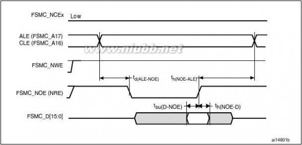
205 STM32F205xx207xx参考手册
STM32F205xx, STM32F207xxElectrical characteristics
Table 74.
Symboltd(D-NWE)(2)tw(NOE)(2)tsu(D-NOE)(2)th(NOE-D)(2)tw(NWE)(2)tv(NWE-D)(2)th(NWE-D)(2)
Switching characteristics for NAND Flash read and write cycles(1)
Parameter
FSMC_D[15:0] valid before FSMC_NWE highFSMC_NOE low width
FSMC_D[15:0] valid data before FSMC_NOE high
Min6THCLK + 12
Max
Unit ns
4THCLK – 1.54THCLK + 1.5 ns25
ns ns
4THCLK + 2.5 ns0
10THCLK + 4
ns ns
3THCLK + 1.5 ns
3THCLK + 4.5
3THCLK + 2
3THCLK + 4.5
ns ns ns
FSMC_D[15:0] valid data after FSMC_NOE high7FSMC_NWE low width
FSMC_NWE low to FSMC_D[15:0] validFSMC_NWE high to FSMC_D[15:0] invalid
4THCLK – 1
td(ALE-NWE)(3)FSMC_ALE valid before FSMC_NWE lowth(NWE-ALE)(3)FSMC_NWE high to FSMC_ALE invalidtd(ALE-NOE)(3)FSMC_ALE valid before FSMC_NOE lowth(NOE-ALE)(3)FSMC_NWE high to FSMC_ALE invalid
1.CL = 15 pF.
2.Based on characterization, not tested in production.3.Guaranteed by design, not tested in production.
5.3.24 Camera interface (DCMI) timing specifications
Table 75.
Symbol
DCMI characteristics
Parameter
Frequency ratio
DCMI_PIXCLK/fHCLK
ConditionsDCMI_PIXCLK= 48MHz
Min
Max2.5
Unit
Doc ID 15818 Rev 5123/147
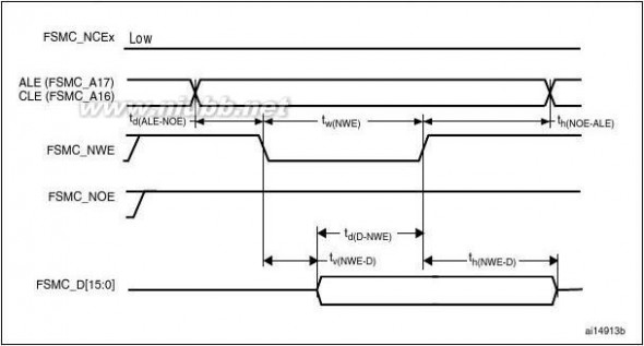
205 STM32F205xx207xx参考手册
Electrical characteristicsSTM32F205xx, STM32F207xx
5.3.25 SD/SDIO MMC card host interface (SDIO) characteristics
Unless otherwise specified, the parameters given in Table76 are derived from tests
performed under ambient temperature, fPCLKx frequency and VDD supply voltage conditions summarized in Table10.
Refer to Section5.3.14: I/O port characteristics for more details on the input/output alternate function characteristics (D[7:0], CMD, CK).
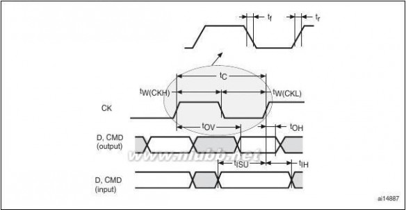
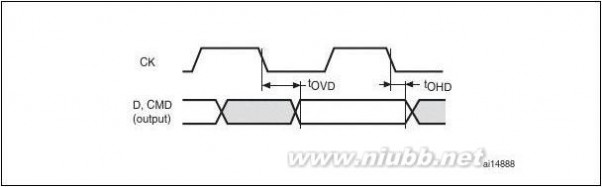
Table 76.
SymbolfPP-
SD / MMC characteristics
Parameter
Clock frequency in data transfer mode
SDIO_CK/fPCLK2 frequency ratio
ConditionsCL ≤ 30 pF-Min0-Max488/3
UnitMHz-
124/147Doc ID 15818 Rev 5
205 STM32F205xx207xx参考手册
STM32F205xx, STM32F207xx
Table 76.
SymboltW(CKL)tW(CKH)
trtf
Electrical characteristics
SD / MMC characteristics (continued)
Parameter
Clock low time, fPP = 16MHzClock high time, fPP = 16MHzClock rise timeClock fall time
ConditionsCL ≤ 30 pFCL ≤ 30 pFCL ≤ 30 pFCL ≤ 30 pF
Min3231
3.55
ns
Max
Unit
CMD, D inputs (referenced to CK)
tISUtIH
Input setup timeInput hold time
CL ≤ 30 pFCL ≤ 30 pF
20
ns
CMD, D outputs (referenced to CK) in MMC and SD HS mode
tOVtOH
Output valid timeOutput hold time
CL ≤ 30 pFCL ≤ 30 pF
0.3
6
ns
CMD, D outputs (referenced to CK) in SD default mode(1)
tOVDtOHD
Output valid default timeOutput hold default time
CL ≤ 30 pFCL ≤ 30 pF
0.5
7
ns
1.Refer to SDIO_CLKCR, the SDI clock control register to control the CK output.
5.3.26 RTC characteristics
Table 77.
Symbol
-
RTC characteristics
Parameter
fPCLK1/RTCCLK frequency
ratio
ConditionsAny read/write
operation from/to an RTC register
Min4
Max-Unit-
Doc ID 15818 Rev 5125/147
205 STM32F205xx207xx参考手册
Package characteristicsSTM32F205xx, STM32F207xx6 Package characteristics
6.1 Package mechanical data
In order to meet environmental requirements, ST offers these devices in different grades of
ECOPACK? packages, depending on their level of environmental compliance. ECOPACK?
specifications, grade definitions and product status are available at: www.st.com.
ECOPACK? is an ST trademark.
126/147Doc ID 15818 Rev 5
205 STM32F205xx207xx参考手册
STM32F205xx, STM32F207xx
Package characteristics
Figure 66.Recommended footprint(1)(2)
Figure 65.LQFP64 – 10 x 10 mm 64 pin low-profile
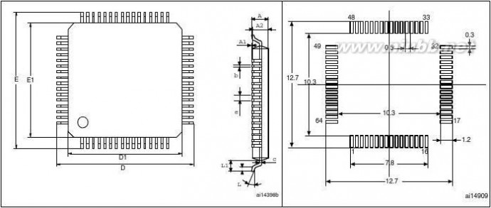
(1)
1.Drawing is not to scale.2.Dimensions are in millimeters.
Table 78.
Symbol
LQFP64 – 10 x 10 mm 64 pin low-profile quad flat package mechanical data
millimeters
扩展:stm32f207参考手册 / stm32f205参考手册 / stm32f207编程参考
Min
Typ
Max
Min
inches(1)
Typ
Max0.0630
0.00200.05310.00670.0035
0.47240.39370.47240.39370.0197
7°0.750
0°0.0177
3.5°0.02360.0394
7°0.0295
0.05510.0087
0.00590.05710.01060.0079
AA1A2bc
1
EE1eθLL1N
1.6000.0501.3500.1700.090
1.4000.220
0.1501.4500.270
0.500
0°0.450
3.5°0.600
Number of pins
64
1.Values in inches are converted from mm and rounded to 4 decimal digits.
Doc ID 15818 Rev 5127/147
205 STM32F205xx207xx参考手册
Package characteristicsSTM32F205xx, STM32F207xx
1.Drawing is not to scale.
Table 79.WLCSP64+2 - 0.400 mm pitch wafer level chip size package mechanical data
millimeters
inches
Max0.6200.2100.4100.3003.6944.026
Typ0.02240.00750.01500.01060.14460.1577
Min0.02050.00670.01380.00940.14390.1569
0.0020
Max0.02440.00830.01610.01180.14540.1585
Symbol
Typ
AA1A2bDEee1FGeee
0.5700.1900.3800.2703.6744.0060.4003.2000.2370.403
Min0.5200.1700.3500.2403.6543.986
0.01570.12600.00930.01590.050
128/147Doc ID 15818 Rev 5
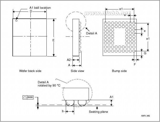
205 STM32F205xx207xx参考手册
STM32F205xx, STM32F207xx
Package characteristics
Figure 69.Recommended footprint(1)(2)
Figure 68.LQFP100, 14 x 14 mm 100-pin low-profile
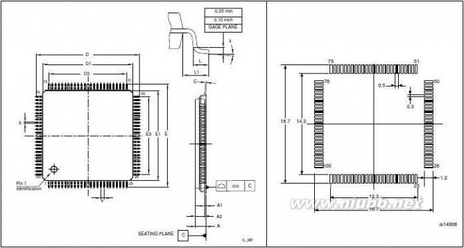
(1)
1.Drawing is not to scale.2.Dimensions are in millimeters.
Table 80.
Symbol
LQPF100 – 14 x 14 mm 100-pin low-profile quad flat package mechanical data
millimeters
Min
Typ
Max1.600
0.0501.3500.1700.09015.80013.80015.80v13.800
16.00014.00012.00016.00014.00012.0000.500
0.4500°
0.6001.0003.5°0.080
7°
0°
0.750
0.0177
16.20014.200
0.62200.5433
1.4000.220
0.1501.4500.2700.20016.20014.200
0.00200.05310.00670.00350.62200.5433
0.62990.55120.47240.62990.55120.47240.01970.02360.03943.5°0.0031
7°0.02950.63780.5591
0.05510.0087
Min
inches(1)
Typ
Max0.06300.00590.05710.01060.00790.63780.5591
AA1A2bcDD1D3EE1E3eLL1kccc
1.Values in inches are converted from mm and rounded to 4 decimal digits.
Doc ID 15818 Rev 5129/147
205 STM32F205xx207xx参考手册
Package characteristics
STM32F205xx, STM32F207xxFigure 71.Recommended
(1)(2)
Figure 70.LQFP144, 20 x 20 mm, 144-pin low-profile quad
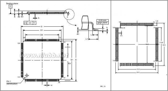
(1)
1.Drawing is not to scale.2.Dimensions are in millimeters.
Table 81.
Symbol
LQFP144, 20 x 20 mm, 144-pin low-profile quad flat package mechanical data
millimeters
Min
Typ
Max1.600
0.0501.3500.1700.09021.80019.80021.80019.800
22.00020.00017.50022.00020.00017.5000.500
0.4500°
0.6001.0003.5°0.080
7°
0°
0.750
0.0177
22.20020.200
0.85830.7795
1.4000.220
0.1501.4500.2700.20022.20020.200
0.00200.05310.00670.00350.85830.7795
0.86610.78740.6890.86610.78740.68900.01970.02360.03943.5°0.0031
7°0.02950.87400.7953
0.05510.0087
Min
inches(1)
Typ
Max0.06300.00590.05710.01060.00790.8740.7953
AA1A2bcDD1D3EE1E3eLL1kccc
1.Values in inches are converted from mm and rounded to 4 decimal digits.
130/147Doc ID 15818 Rev 5
205 STM32F205xx207xx参考手册
STM32F205xx, STM32F207xxPackage characteristics
1.Drawing is not to scale.
Table 82.
Symbol
LQFP176 - Low profile quad flat package 24 × 24 × 1.4 mm package mechanical data
millimeters
Min
Typ
Max1.600
0.0501.3500.1700.09023.90023.900
0.500
25.90025.9000.450
1.0001.2501.250
0°
0.080
7°
0°
0.0031
26.10026.1000.750
1.01971.01970.0177
0.03940.04920.0492
7°
0.1501.4500.2700.20024.10024.100
0.00200.05310.00670.00350.94090.9409
0.0197
1.02761.02760.0295
Min
inches(1)
Typ
Max0.06300.00590.05710.01060.00790.94880.9488
AA1A2bcDEeHDHEL(2)L1ZDZEkccc
1.Values in inches are converted from mm and rounded to 4 decimal digits.2.L dimension is measured at gauge plane at 0.25 mm above the seating plane.
Doc ID 15818 Rev 5131/147
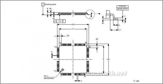
205 STM32F205xx207xx参考手册
Package characteristicsSTM32F205xx, STM32F207xx
1.Drawing is not to scale.
扩展:stm32f207参考手册 / stm32f205参考手册 / stm32f207编程参考
Table 83.
Symbol
UFBGA176+25 - ultra thin fine pitch ball grid array 10 × 10 × 0.6 mm mechanical data
millimeters
Min
Typ0.5300.0800.4500.130
0.2700.3009.9509.9500.6000.400
0.3200.35010.00010.0000.6500.4500.1200.1500.080
0.3700.40010.05010.0500.7000.500
0.01060.01180.37400.37400.02360.0157
Max0.6100.1100.500
Min0.01810.0020.0157
inches(1)
Typ0.02090.00310.01770.00510.01260.01380.39370.39370.02560.01770.00470.00590.0031
0.01460.01570.39570.39570.02760.0197Max0.02400.00430.0197
AA1A2A3A4bDEeFdddeeefff
0.4600.0500.400
1.Values in inches are converted from mm and rounded to 4 decimal digits.
132/147Doc ID 15818 Rev 5
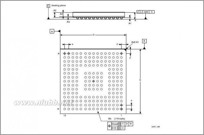
205 STM32F205xx207xx参考手册
STM32F205xx, STM32F207xxPackage characteristics
6.2 Thermal characteristics
The maximum chip-junction temperature, TJ max, in degrees Celsius, may be calculated
using the following equation:
TJ max = TA max + (PD max x ΘJA)
Where:
●
●
●
●TA max is the maximum ambient temperature in °C,ΘJA is the package junction-to-ambient thermal resistance, in °C/W,PD max is the sum of PINT max and PI/O max (PD max = PINT max + PI/Omax),PINT max is the product of IDD and VDD, expressed in Watts. This is the maximum chip
internal power.
PI/O max = Σ (VOL × IOL) + Σ((VDD – VOH) × IOH),PI/O max represents the maximum power dissipation on output pins where:
taking into account the actual VOL / IOL and VOH / IOH of the I/Os at low and high level in the
application.
Table 84.
Symbol Package thermal characteristicsParameter
Thermal resistance junction-ambient
LQFP 64 - 10 × 10 mm / 0.5 mm pitch
Thermal resistance junction-ambient
WLCSP64+2 - 0.400 mm pitch
Thermal resistance junction-ambient
LQFP 100 - 14 × 14 mm / 0.5 mm pitch
Thermal resistance junction-ambient
LQFP 144 - 20 × 20 mm / 0.5 mm pitch
Thermal resistance junction-ambient
LQFP 176 - 24 × 24 mm / 0.5 mm pitch
Thermal resistance junction-ambient
UFBGA176 - 10× 10 mm / 0.5 mm pitchValue455146°C/W40UnitΘJA3839
Reference document
JESD51-2 Integrated Circuits Thermal Test Method Environment Conditions - Natural
Convection (Still Air). Available from www.jedec.org.Doc ID 15818 Rev 5133/147
205 STM32F205xx207xx参考手册
Part numberingSTM32F205xx, STM32F207xx7 Part numbering
Table 85.
Example:
Device family
Product type
Device subfamily
207= STM32F20x, connectivity, USB OTG FS/HS, camera
interface,, Ethernet
Pin count
V = 100 pins
Z = 144 pins
I = 176 pins(2)
Flash memory size
C = 256 Kbytes of Flash memory
E = 512 Kbytes of Flash memory
F = 768 Kbytes of Flash memory
G = 1024 Kbytes of Flash memory
Package
T = LQFP
H = UFBGA
Y = WLCSP
Temperature range
7 = Industrial temperature range, –40 to 105 °C.
Options
TR = tape and reel
1.The 66 pins is available on WLCSP package only.
2.The LQFP176 package is not in production. It is available only for development. Ordering information schemeSTM32F205RET6xxxFor a list of available options (speed, package, etc.) or for further information on any aspect
of this device, please contact your nearest ST sales office.
134/147Doc ID 15818 Rev 5
205 STM32F205xx207xx参考手册
STM32F205xx, STM32F207xxApplication block diagrams
Appendix A
A.1
Table 86.
Application block diagrams
Main applications versus package
Table86 gives examples of configurations for each package.
Main applications versus package for STM32F207xx microcontrollers(1)
64 pins100 pins144 pins176 pins
Config Config Config Config ConfigConfigConfig ConfigConfig ConfigConfigConfigConfig1231234123412
OTG
FSFSHS ULPI
USB 2
OTGFSFS
EthernetSPI/I2S2SPI/I2S3SDIO
SDIO8bits Data10bits Data12bits Data14bits DataNOR/RAM Muxed
FSMC
NOR/RAMNANDCF
CAN
--MIIRMII
XX------XX-----X
XX--------------XXXXX---X-XX
XXXX
XXXXXXXX-XX
XXXXXXX
SDIOor DCMI
XX-XX--X-XXXXX
XXXX
XXXX
XXXXXXXXX
XX
X
XXXXXXXXXXXXX
XXXXXXXXXXX
USB 1
SDIO or DCMISDIO or DCMISDIO or DCMISDIO or DCMISDIO or DCMISDIO or DCMI
DCMI
---XXXXXXXXXX
----
---X
---X
X--X-X
X*2219-X
-X
XXX-
XX*19X-
XX*22XX
XX*19XX
XX*22X-
XX*22XX
1.X*y: FSMC address limited to “y”.
Doc ID 15818 Rev 5135/147
205 STM32F205xx207xx参考手册 扩展:stm32f207参考手册 / stm32f205参考手册 / stm32f207编程参考
Application block diagramsSTM32F205xx, STM32F207xx
A.2 Application example with regulator off
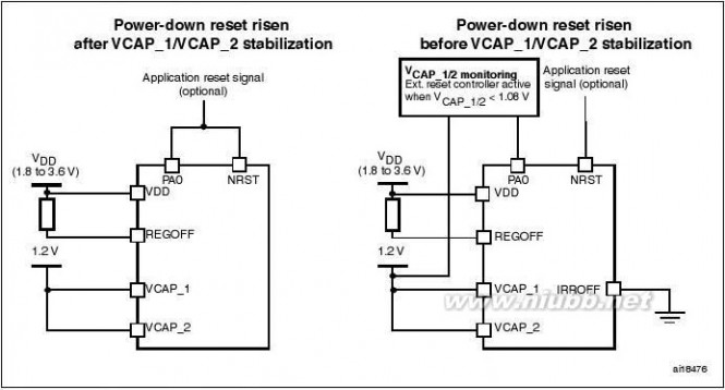
1.This mode is available only on UFBGA176 and WLCSP64+2 packages.
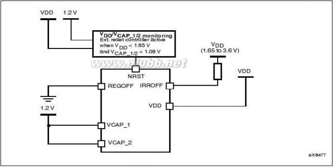
1.This mode is available only on WLCSP64+2 package.
136/147Doc ID 15818 Rev 5
205 STM32F205xx207xx参考手册
STM32F205xx, STM32F207xxApplication block diagrams
A.3 USB OTG full speed (FS) interface solutions

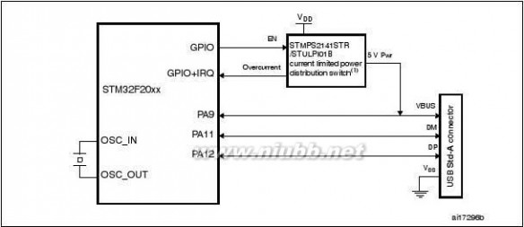
1.STMPS2141STR/STULPI01B needed only if the application has to support a VBUS powered device. A
basic power switch can be used if 5 V are available on the application board.
Doc ID 15818 Rev 5137/147
205 STM32F205xx207xx参考手册
Application block diagramsSTM32F205xx, STM32F207xx
1.External voltage regulator only needed when building a VBUS powered device.
2.STMPS2141STR/STULPI01B needed only if the application has to support a VBUS powered device. A
basic power switch can be used if 5V are available on the application board.3.The same application can be developped using the OTG HS in FS mode to achieve enhanced
performance thanks to the large Rx/Tx FIFO and to a dedicated DMA controller.
A.4 USB OTG high speed (HS) interface solutions
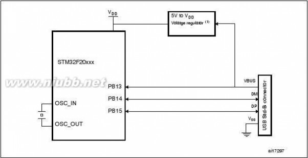
138/147Doc ID 15818 Rev 5

205 STM32F205xx207xx参考手册
STM32F205xx, STM32F207xx
Application block diagrams
1.STMPS2141STR/STULPI01B needed only if the application has to support a VBUS powered device. A
basic power switch can be used if 5 V are available on the application board.

1.It is possible to use MCO1 or MCO2 to save a crystal. It is however not mandatory to clock the STM32F20x
with a 24 or 26MHz crystal when using USB HS. The above figure only shows an example of a possible connection.
Doc ID 15818 Rev 5139/147
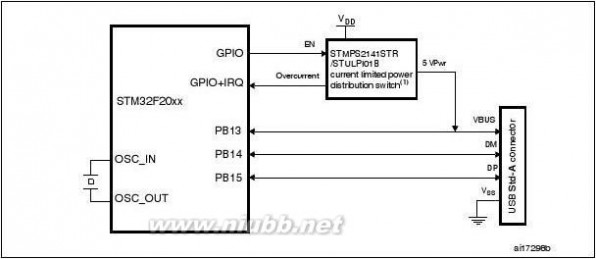
205 STM32F205xx207xx参考手册
Application block diagramsSTM32F205xx, STM32F207xx
A.5 Complete audio player solutions
Two solutions are offered, illustrated in Figure82 and Figure83.
Figure82 shows storage media to audio DAC/amplifier streaming using a software Codec. This solution implements an audio crystal to provide audio class I2S accuracy on the master clock (0.5% error maximum, see the Serial peripheral interface section in the reference manual for details).
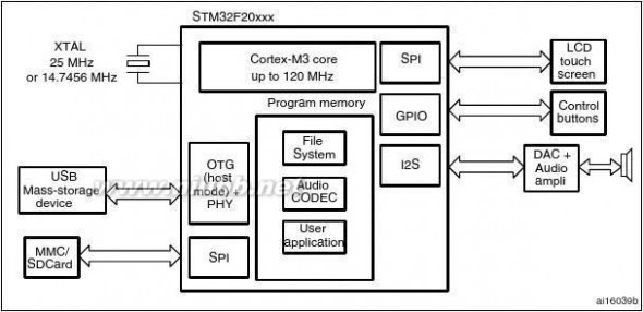
Figure83 shows storage media to audio Codec/amplifier streaming with SOF synchronization of input/output audio streaming using a hardware Codec.
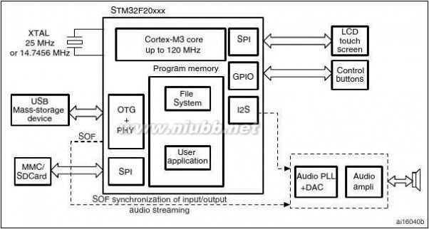
140/147Doc ID 15818 Rev 5
205 STM32F205xx207xx参考手册
STM32F205xx, STM32F207xxApplication block diagrams
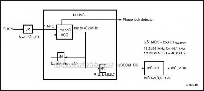
Doc ID 15818 Rev 5141/147
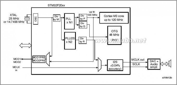
205 STM32F205xx207xx参考手册
Application block diagramsSTM32F205xx, STM32F207xx1.I2S_SCK is the I2S serial clock to the external audio DAC (not to be confused with I2S_CK).
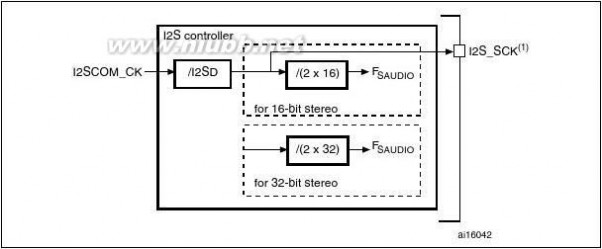
1.I2S_SCK is the I2S serial clock to the external audio DAC (not to be confused with I2S_CK).
142/147Doc ID 15818 Rev 5
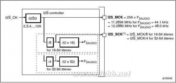
205 STM32F205xx207xx参考手册
STM32F205xx, STM32F207xxRevision historyRevision history
Table 87.
Date
05-Jun-2009 Document revision historyRevision1Initial release.
Document status promoted from Target specification to Preliminary
data.
In Table5: STM32F20x pin and ball definitions:
–Note4 updated
–VDD_SA and VDD_3 pins inverted (Figure11: STM32F20x LQFP100
pinout, Figure12: STM32F20x LQFP144 pinout and Figure13:
扩展:stm32f207参考手册 / stm32f205参考手册 / stm32f207编程参考
STM32F20x LQFP176 pinout corrected accordingly).
Section6.1: Package mechanical data changed to LQFP with no
exposed pad.
LFBGA144 package removed. STM32F203xx part numbers removed.
Part numbers with 128 and 256 Kbyte Flash densities added.
Encryption features removed.
PC13-TAMPER-RTC renamed to PC13-RTC_AF1 and PI8-TAMPER-
RTC renamed to PI8-RTC_AF2.Changes09-Oct-2009201-Feb-20103
Doc ID 15818 Rev 5143/147
205 STM32F205xx207xx参考手册
Revision historyTable 87.
DateSTM32F205xx, STM32F207xxDocument revision history (continued)RevisionChanges
Renamed high-speed SRAM, system SRAM.
Removed combination: 128KBytes Flash memory in LQFP144.Added UFBGA176 package. Added note 1 related to LQFP176 package in Table2, Figure13, and Table85.
Added information on ART accelerator and audio PLL (PLLI2S).Added Table4: USART feature comparison.
Several updates on Table5: STM32F20x pin and ball definitions and Table6: Alternate function mapping. ADC, DAC, oscillator, RTC_AF, WKUP and VBUS signals removed from alternate functions and
moved to the “other functions” column in Table5: STM32F20x pin and ball definitions.
TRACESWO added in Figure4: STM32F20x block diagram, Table5: STM32F20x pin and ball definitions, and Table6: Alternate function mapping.
XTAL oscillator frequency updated on cover page, in Figure4: STM32F20x block diagram and in Section2.2.12: External interrupt/event controller (EXTI).
Updated list of peripherals used for boot mode in Section2.2.14: Boot modes.
Added Regulator bypass mode in Section2.2.17: Voltage regulator, and Section5.3.3: Operating conditions at power-up / power-down in regulator bypass mode.
Updated Section2.2.18: Real-time clock (RTC), backup SRAM and backup registers.
Added NoteNote: in Section2.2.19: Low-power modes.
Added SPI TI protocol in Section2.2.28: Serial peripheral interface (SPI).
Added USB OTG_FS features in Section2.2.33: Universal serial bus on-the-go full-speed (OTG_FS).
Updated VCAP_1 and VCAP_2 capacitor value to 2.2μF in Figure18: Power supply scheme.
Removed DAC, modified ADC limitations, and updated I/O
compensation for 1.8 to 2.1V range in Table11: Limitations depending on the operating power supply range.
Added VBORL, VBORM, VBORH and IRUSH in Table14: Embedded reset and power control block characteristics.
Removed table Typical current consumption in Sleep mode with Flash memory in Deep power down mode. Merged typical and maximum current consumption sections and added Table15: Typical and maximum current consumption in Run mode, code with data processing running from Flash, Table16: Typical and maximum
current consumption in Run mode, code with data processing running from RAM, Table17: Typical and maximum current consumption in Sleep mode, Table18: Typical and maximum current consumptions in Stop mode, Table19: Typical and maximum current consumptions in Standby mode, and Table20: Typical and maximum current consumptions in VBAT mode.
Update Table29: Main PLL characteristics and added Section5.3.10: PLL spread spectrum clock generation (SSCG) characteristics.13-Jul-20104
144/147Doc ID 15818 Rev 5
205 STM32F205xx207xx参考手册
STM32F205xx, STM32F207xxTable 87.
DateRevision historyDocument revision history (continued)RevisionChanges13-Jul-2010Added Note6 for CIO in Table40: I/O static characteristics.Updated Section5.3.16: TIM timer characteristics.Added TNRST_OUT in Table43: NRST pin characteristics.Updated Table46: I2C characteristics.Removed 8-bit data in and data out waveforms from Figure36: ULPI timing diagram.Removed note related to ADC calibration in Table60. Section5.3.18: 12-bit ADC characteristics: ADC characteristics tables merged into one single table; tables ADC conversion time and ADC accuracy removed.Updated Table61: DAC characteristics.Updated Section5.3.20: Temperature sensor characteristics and Section5.3.21: VBAT monitoring characteristics.Update Section5.3.24: Camera interface (DCMI) timing specifications.4
(continued)Added Section5.3.25: SD/SDIO MMC card host interface (SDIO)
characteristics, and Section5.3.26: RTC characteristics.
Added Section6.2: Thermal characteristics. Updated Table82:
LQFP176 - Low profile quad flat package 24 × 24 × 1.4 mm package mechanical data and Figure72: LQFP176 - Low profile quad flat package 24 × 24 × 1.4 mm, package outline.
Changed tape and reel code to TX in Table85: Ordering information scheme.
Added Table86: Main applications versus package for STM32F207xx microcontrollers. Updated figures in Appendix A.3: USB OTG full speed (FS) interface solutions and A.4: USB OTG high speed (HS) interface solutions. Updated Figure84: Audio player solution using PLL, PLLI2S, USB and 1 crystal and Figure85: Audio PLL (PLLI2S) providing accurate I2S clock.
扩展:stm32f207参考手册 / stm32f205参考手册 / stm32f207编程参考
Doc ID 15818 Rev 5145/147
205 STM32F205xx207xx参考手册
Revision historyTable 87.
DateSTM32F205xx, STM32F207xxDocument revision history (continued)RevisionChanges
Update I/Os in Section: Features.
Added WLCSP66(64+2) package. Added note 1 related to LQFP176 on cover page.
Added trademark for ART accelerator. Updated Section2.2.3: Adaptive real-time memory accelerator (ART Accelerator?).Updated Figure5: Multi-AHB matrix.
Added case of BOR inactivation using IRROFF on WLCSP devices in Section2.2.16: Power supply supervisor.
Reworked Section2.2.17: Voltage regulator to clarify regulator off modes. Renamed PDROFF, IRROFF in the whole document.Added Section2.2.20: VBAT operation.
Updated LIN and IrDA features for UART4/5 in Table4: USART feature comparison.
Table5: STM32F20x pin and ball definitions: Modified VDD_3 pin, and added note related to the FSMC_NL pin; renamed BYPASS-REG REGOFF, and add IRROFF pin; renamed USART4/5 UART4/5. USART4 pins renamed UART4.
Changed VSS_SA to VSS, and VDD_SA pin reserved for future use. Updated maximum HSE crystal frequency to 26MHz.
Section5.2: Absolute maximum ratings: Updated VIN minimum and maximum values and note for non-five-volt tolerant pins in Table7: Voltage characteristics. Updated IINJ(PIN) maximum values and related notes in Table8: Current characteristics.
Updated VDDA minimum value in Table10: General operating conditions.
Added Note2 Updated Maximum CPU frequency in Table11: Limitations depending on the operating power supply range, and added Figure20: Number of wait states versus fCPU and VDD range.Added brownout level 1, 2, and 3 thresholds in Table14: Embedded reset and power control block characteristics.
Changed fOSC_IN maximum value in Table24: HSE 4-26 MHz oscillator characteristics.
Changed fPLL_IN maximum value in Table29: Main PLL characteristics, and updated jitter parameters in Table30: PLLI2S (audio PLL) characteristics.
Section5.3.14: I/O port characteristics: updated VIH and VIL in Table40: I/O static characteristics.
Added Note1 below Table41: Output voltage characteristics.Updated RPD and RPU parameter description in Table51: USB OTG FS DC electrical characteristics.
Updated VREF+ minimum value in Table59: ADC characteristics.Updated Table64: Embedded internal reference voltage.
Removed Ethernet and USB2 for 64-pin devices in Table86: Main applications versus package for STM32F207xx microcontrollers.
Added A.2: Application example with regulator off, removed “OTG FS connection with external PHY” figure, updated Figure77, Figure78, and Figure80 to add STULPI01B.25-Nov-20105
146/147Doc ID 15818 Rev 5
205 STM32F205xx207xx参考手册
STM32F205xx, STM32F207xx
Please Read Carefully:
Information in this document is provided solely in connection with ST products. STMicroelectronics NV and its subsidiaries (“ST”) reserve theright to make changes, corrections, modifications or improvements, to this document, and the products and services described herein at anytime, without notice.
All ST products are sold pursuant to ST’s terms and conditions of sale.
Purchasers are solely responsible for the choice, selection and use of the ST products and services described herein, and ST assumes noliability whatsoever relating to the choice, selection or use of the ST products and services described herein.
No license, express or implied, by estoppel or otherwise, to any intellectual property rights is granted under this document. If any part of thisdocument refers to any third party products or services it shall not be deemed a license grant by ST for the use of such third party productsor services, or any intellectual property contained therein or considered as a warranty covering the use in any manner whatsoever of suchthird party products or services or any intellectual property contained therein.
UNLESS OTHERWISE SET FORTH IN ST’S TERMS AND CONDITIONS OF SALE ST DISCLAIMS ANY EXPRESS OR IMPLIEDWARRANTY WITH RESPECT TO THE USE AND/OR SALE OF ST PRODUCTS INCLUDING WITHOUT LIMITATION IMPLIEDWARRANTIES OF MERCHANTABILITY, FITNESS FOR A PARTICULAR PURPOSE (AND THEIR EQUIVALENTS UNDER THE LAWSOF ANY JURISDICTION), OR INFRINGEMENT OF ANY PATENT, COPYRIGHT OR OTHER INTELLECTUAL PROPERTY RIGHT.
UNLESS EXPRESSLY APPROVED IN WRITING BY AN AUTHORIZED ST REPRESENTATIVE, ST PRODUCTS ARE NOTRECOMMENDED, AUTHORIZED OR WARRANTED FOR USE IN MILITARY, AIR CRAFT, SPACE, LIFE SAVING, OR LIFE SUSTAININGAPPLICATIONS, NOR IN PRODUCTS OR SYSTEMS WHERE FAILURE OR MALFUNCTION MAY RESULT IN PERSONAL INJURY,DEATH, OR SEVERE PROPERTY OR ENVIRONMENTAL DAMAGE. ST PRODUCTS WHICH ARE NOT SPECIFIED AS "AUTOMOTIVEGRADE" MAY ONLY BE USED IN AUTOMOTIVE APPLICATIONS AT USER’S OWN RISK.
Resale of ST products with provisions different from the statements and/or technical features set forth in this document shall immediately voidany warranty granted by ST for the ST product or service described herein and shall not create or extend in any manner whatsoever, anyliability of ST.
扩展:stm32f207参考手册 / stm32f205参考手册 / stm32f207编程参考
ST and the ST logo are trademarks or registered trademarks of ST in various countries.
Information in this document supersedes and replaces all information previously supplied.
The ST logo is a registered trademark of STMicroelectronics. All other names are the property of their respective owners.
? 2010 STMicroelectronics - All rights reserved
STMicroelectronics group of companies
Australia - Belgium - Brazil - Canada - China - Czech Republic - Finland - France - Germany - Hong Kong - India - Israel - Italy - Japan - Malaysia - Malta - Morocco - Philippines - Singapore - Spain - Sweden - Switzerland - United Kingdom - United States of America
www.st.com
Doc ID 15818 Rev 5147/147
扩展:stm32f207参考手册 / stm32f205参考手册 / stm32f207编程参考
三 : STM32F205xx207xx参考手册
STM32F205xxSTM32F207xx
ARM-based 32-bit MCU, 150DMIPs, up to 1 MB Flash/128+4KB RAM,USB OTG HS/FS, Ethernet, 17 TIMs, 3 ADCs, 15 comm. interfaces & camera
Preliminary data
Features
■
■
■
■
■
■■
■
■
Core: ARM 32-bit Cortex?-M3 CPU with Adaptive real-time accelerator (ART
Accelerator?) allowing 0-wait state execution performance from Flash memory, frequency up to 120MHz, memory protection unit,
150DMIPS/1.25DMIPS/MHz (Dhrystone 2.1)Memories
–Up to 1 Mbyte of Flash memory–Up to 128 + 4 Kbytes of SRAM
–Flexible static memory controller that
supports Compact Flash, SRAM, PSRAM, NOR and NAND memories
–LCD parallel interface, 8080/6800 modesClock, reset and supply management
–1.8 to 3.6 V application supply and I/Os–POR, PDR, PVD and BOR–4 to 26 MHz crystal oscillator
–Internal 16MHz factory-trimmed RC (1% accuracy)
–32kHz oscillator for RTC with calibration–Internal 32kHz RC with calibrationLow power
–Sleep, Stop and Standby modes
–VBAT supply for RTC, 20 × 32 bit backup registers, and optional 4 KB backup SRAM3 × 12-bit, 0.5 μs A/D converters–up to 24 channels
–up to 6 MSPS in triple interleaved mode2 × 12-bit D/A convertersGeneral-purpose DMA
–16-stream DMA controller with centralized FIFOs and burst supportUp to 17 timers
–Up to twelve 16-bit and two 32-bit timers, each with up to 4 IC/OC/PWM or pulse counter and quadrature (incremental) encoder inputDebug mode
–Serial wire debug (SWD) & JTAG interfaces–Cortex-M3 Embedded Trace Macrocell?
1.Package not in production (for development only).■
■
■
■■■
Up to 140 I/O ports with interrupt capability:–Up to 136 fast I/Os up to 60MHz–Up to 138 5V-tolerant I/Os
Up to 15 communication interfaces
–Up to 3 × I2C interfaces (SMBus/PMBus)–Up to 4 USARTs and 2 UARTs (7.5 Mbit/s, ISO 7816 interface, LIN, IrDA, modem control)
–Up to 3 SPIs (30 Mbit/s), 2 with muxed I2S to achieve audio class accuracy via audio PLL or external PLL
–2 × CAN interfaces (2.0B Active)–SDIO interface
Advanced connectivity
–USB 2.0 full-speed device/host/OTG controller with on-chip PHY–USB 2.0 high-speed/full-speed
device/host/OTG controller with dedicated DMA, on-chip full-speed PHY and ULPI–10/100 Ethernet MAC with dedicated DMA: supports IEEE 1588v2 hardware, MII/RMII8- to 14-bit parallel camera interface: up to 27Mbyte/s at 27MHz or 48 Mbyte/s at 48 MHzCRC calculation unit, 96-bit unique IDAnalog true random number generator
Device summary
Part number
STM32F205RB, STM32F205RC, STM32F205RE, STM32F205RF, STM32F205RG, STM32F205VB, STM32F205VC, STM32F205VE, STM32F205VF STM32F205VG, STM32F205ZC, STM32F205ZE, STM32F205ZF, STM32F205ZG
STM32F207IC, STM32F207IE, STM32F207IF, STM32F207IG, STM32F207ZC, STM32F207ZE, STM32F207ZF, STM32F207ZG, STM32F207VC, STM32F207VE, STM32F207VF, STM32F207VG
Table 1.
Reference
STM32F205xx
STM32F207xx
November 2010Doc ID 15818 Rev 51/147
www.st.com
This is preliminary information on a new product now in development or undergoing evaluation. Details are subject to change without notice.
ContentsSTM32F205xx, STM32F207xxContents
1
2Introduction . . . . . . . . . . . . . . . . . . . . . . . . . . . . . . . . . . . . . . . . . . . . . . . . 9Description . . . . . . . . . . . . . . . . . . . . . . . . . . . . . . . . . . . . . . . . . . . . . . . . 10
2.1
2.2Full compatibility throughout the family . . . . . . . . . . . . . . . . . . . . . . . . . . 13Device overview . . . . . . . . . . . . . . . . . . . . . . . . . . . . . . . . . . . . . . . . . . . . 15
2.2.1
2.2.2
2.2.3
2.2.4
2.2.5
2.2.6
2.2.7
2.2.8
2.2.9
2.2.10
2.2.11
2.2.12
2.2.13
2.2.14
2.2.15
2.2.16
2.2.17
2.2.18
2.2.19
2.2.20
2.2.21
2.2.22
2.2.23
2.2.24
2.2.25
2.2.26
2.2.27
2.2.28ARM? Cortex?-M3 core with embedded Flash and SRAM . . . . . . . . . 16Memory protection unit . . . . . . . . . . . . . . . . . . . . . . . . . . . . . . . . . . . . . 16Adaptive real-time memory accelerator (ART Accelerator?) . . . . . . . . 16Embedded Flash memory . . . . . . . . . . . . . . . . . . . . . . . . . . . . . . . . . . . 16CRC (cyclic redundancy check) calculation unit . . . . . . . . . . . . . . . . . . 17True random number generator (RNG) . . . . . . . . . . . . . . . . . . . . . . . . . 17Embedded SRAM . . . . . . . . . . . . . . . . . . . . . . . . . . . . . . . . . . . . . . . . . 17Multi-AHB bus matrix . . . . . . . . . . . . . . . . . . . . . . . . . . . . . . . . . . . . . . . 17DMA . . . . . . . . . . . . . . . . . . . . . . . . . . . . . . . . . . . . . . . . . . . . . . . . . . . . 18FSMC (flexible static memory controller) . . . . . . . . . . . . . . . . . . . . . . . . 18Nested vectored interrupt controller (NVIC) . . . . . . . . . . . . . . . . . . . . . . 19External interrupt/event controller (EXTI) . . . . . . . . . . . . . . . . . . . . . . . 19Clocks and startup . . . . . . . . . . . . . . . . . . . . . . . . . . . . . . . . . . . . . . . . . 19Boot modes . . . . . . . . . . . . . . . . . . . . . . . . . . . . . . . . . . . . . . . . . . . . . . 20Power supply schemes . . . . . . . . . . . . . . . . . . . . . . . . . . . . . . . . . . . . . 20Power supply supervisor . . . . . . . . . . . . . . . . . . . . . . . . . . . . . . . . . . . . 20Voltage regulator . . . . . . . . . . . . . . . . . . . . . . . . . . . . . . . . . . . . . . . . . . 20Real-time clock (RTC), backup SRAM and backup registers . . . . . . . . 23Low-power modes . . . . . . . . . . . . . . . . . . . . . . . . . . . . . . . . . . . . . . . . . 23VBAT operation . . . . . . . . . . . . . . . . . . . . . . . . . . . . . . . . . . . . . . . . . . . . 24Timers and watchdogs . . . . . . . . . . . . . . . . . . . . . . . . . . . . . . . . . . . . . . 24Basic timers TIM6 and TIM7 . . . . . . . . . . . . . . . . . . . . . . . . . . . . . . . . . 26Independent watchdog . . . . . . . . . . . . . . . . . . . . . . . . . . . . . . . . . . . . . 26Window watchdog . . . . . . . . . . . . . . . . . . . . . . . . . . . . . . . . . . . . . . . . . 26SysTick timer . . . . . . . . . . . . . . . . . . . . . . . . . . . . . . . . . . . . . . . . . . . . . 27I2C bus . . . . . . . . . . . . . . . . . . . . . . . . . . . . . . . . . . . . . . . . . . . . . . . . . . 27Universal synchronous/asynchronous receiver transmitters(UARTs/USARTs) . . . . . . . . . . . . . . . . . . . . . . . . . . . . . . . . . . . . . . . . . 27Serial peripheral interface (SPI) . . . . . . . . . . . . . . . . . . . . . . . . . . . . . . . 28
2/147Doc ID 15818 Rev 5
STM32F205xx, STM32F207xx2.2.29
2.2.30
2.2.31
2.2.32
2.2.33
2.2.34
2.2.35
2.2.36
2.2.37
2.2.38
2.2.39
2.2.40
2.2.41
2.2.42ContentsInter-integrated sound (I2S) . . . . . . . . . . . . . . . . . . . . . . . . . . . . . . . . . . 28SDIO . . . . . . . . . . . . . . . . . . . . . . . . . . . . . . . . . . . . . . . . . . . . . . . . . . . 28Ethernet MAC interface with dedicated DMA and IEEE1588 support . 29Controller area network (CAN) . . . . . . . . . . . . . . . . . . . . . . . . . . . . . . . 29Universal serial bus on-the-go full-speed (OTG_FS) . . . . . . . . . . . . . . . 29Universal serial bus on-the-go high-speed (OTG_HS) . . . . . . . . . . . . . 30Audio PLL (PLLI2S) . . . . . . . . . . . . . . . . . . . . . . . . . . . . . . . . . . . . . . . . 30Digital camera interface (DCMI) . . . . . . . . . . . . . . . . . . . . . . . . . . . . . . . 31GPIOs (general-purpose inputs/outputs) . . . . . . . . . . . . . . . . . . . . . . . . 31ADCs (analog-to-digital converters) . . . . . . . . . . . . . . . . . . . . . . . . . . . . 31DAC (digital-to-analog converter) . . . . . . . . . . . . . . . . . . . . . . . . . . . . . . 32Temperature sensor . . . . . . . . . . . . . . . . . . . . . . . . . . . . . . . . . . . . . . . . 32Serial wire JTAG debug port (SWJ-DP) . . . . . . . . . . . . . . . . . . . . . . . . . 32Embedded Trace Macrocell? . . . . . . . . . . . . . . . . . . . . . . . . . . . . . . . . 32
3
4
5Pinouts and pin description . . . . . . . . . . . . . . . . . . . . . . . . . . . . . . . . . . 33Memory mapping . . . . . . . . . . . . . . . . . . . . . . . . . . . . . . . . . . . . . . . . . . 53Electrical characteristics . . . . . . . . . . . . . . . . . . . . . . . . . . . . . . . . . . . . 54
5.1Parameter conditions . . . . . . . . . . . . . . . . . . . . . . . . . . . . . . . . . . . . . . . . 54
5.1.1
5.1.2
5.1.3
5.1.4
5.1.5
5.1.6
5.1.7Minimum and maximum values . . . . . . . . . . . . . . . . . . . . . . . . . . . . . . . 54Typical values . . . . . . . . . . . . . . . . . . . . . . . . . . . . . . . . . . . . . . . . . . . . . 54Typical curves . . . . . . . . . . . . . . . . . . . . . . . . . . . . . . . . . . . . . . . . . . . . 54Loading capacitor . . . . . . . . . . . . . . . . . . . . . . . . . . . . . . . . . . . . . . . . . 54Pin input voltage . . . . . . . . . . . . . . . . . . . . . . . . . . . . . . . . . . . . . . . . . . 54Power supply scheme . . . . . . . . . . . . . . . . . . . . . . . . . . . . . . . . . . . . . . 55Current consumption measurement . . . . . . . . . . . . . . . . . . . . . . . . . . . 55
5.2
5.3Absolute maximum ratings . . . . . . . . . . . . . . . . . . . . . . . . . . . . . . . . . . . . 56Operating conditions . . . . . . . . . . . . . . . . . . . . . . . . . . . . . . . . . . . . . . . . 57
5.3.1
5.3.2
5.3.3
5.3.4
5.3.5
5.3.6General operating conditions . . . . . . . . . . . . . . . . . . . . . . . . . . . . . . . . . 57Operating conditions at power-up / power-down (regulator not bypassed) . . . . . . . . . . . . . . . . . . . . . . . . . . . . . . . . . . . . 59Operating conditions at power-up / power-down in regulatorbypass mode . . . . . . . . . . . . . . . . . . . . . . . . . . . . . . . . . . . . . . . . . . . . . 60Embedded reset and power control block characteristics . . . . . . . . . . . 60Supply current characteristics . . . . . . . . . . . . . . . . . . . . . . . . . . . . . . . . 61External clock source characteristics . . . . . . . . . . . . . . . . . . . . . . . . . . . 67
Doc ID 15818 Rev 53/147
Contents5.3.7
5.3.8
5.3.9
5.3.10
5.3.11
5.3.12
5.3.13
5.3.14
5.3.15
5.3.16
5.3.17
5.3.18
5.3.19
5.3.20
5.3.21
5.3.22
5.3.23
5.3.24
5.3.25
5.3.26STM32F205xx, STM32F207xxInternal clock source characteristics . . . . . . . . . . . . . . . . . . . . . . . . . . . 71Wakeup time from low-power mode . . . . . . . . . . . . . . . . . . . . . . . . . . . . 71PLL characteristics . . . . . . . . . . . . . . . . . . . . . . . . . . . . . . . . . . . . . . . . 72PLL spread spectrum clock generation (SSCG) characteristics . . . . . . 73Memory characteristics . . . . . . . . . . . . . . . . . . . . . . . . . . . . . . . . . . . . . 75EMC characteristics . . . . . . . . . . . . . . . . . . . . . . . . . . . . . . . . . . . . . . . . 76Absolute maximum ratings (electrical sensitivity) . . . . . . . . . . . . . . . . . 77I/O port characteristics . . . . . . . . . . . . . . . . . . . . . . . . . . . . . . . . . . . . . . 78NRST pin characteristics . . . . . . . . . . . . . . . . . . . . . . . . . . . . . . . . . . . . 82TIM timer characteristics . . . . . . . . . . . . . . . . . . . . . . . . . . . . . . . . . . . . 83Communications interfaces . . . . . . . . . . . . . . . . . . . . . . . . . . . . . . . . . . 8512-bit ADC characteristics . . . . . . . . . . . . . . . . . . . . . . . . . . . . . . . . . . . 98DAC electrical specifications . . . . . . . . . . . . . . . . . . . . . . . . . . . . . . . . 102Temperature sensor characteristics . . . . . . . . . . . . . . . . . . . . . . . . . . . 104VBAT monitoring characteristics . . . . . . . . . . . . . . . . . . . . . . . . . . . . . . 104Embedded reference voltage . . . . . . . . . . . . . . . . . . . . . . . . . . . . . . . . 104FSMC characteristics . . . . . . . . . . . . . . . . . . . . . . . . . . . . . . . . . . . . . . 105Camera interface (DCMI) timing specifications . . . . . . . . . . . . . . . . . . 123SD/SDIO MMC card host interface (SDIO) characteristics . . . . . . . . . 124RTC characteristics . . . . . . . . . . . . . . . . . . . . . . . . . . . . . . . . . . . . . . . 125
6Package characteristics . . . . . . . . . . . . . . . . . . . . . . . . . . . . . . . . . . . . 126
6.1
6.2Package mechanical data . . . . . . . . . . . . . . . . . . . . . . . . . . . . . . . . . . . 126Thermal characteristics . . . . . . . . . . . . . . . . . . . . . . . . . . . . . . . . . . . . . 133
7Part numbering . . . . . . . . . . . . . . . . . . . . . . . . . . . . . . . . . . . . . . . . . . . 134Appendix AApplication block diagrams . . . . . . . . . . . . . . . . . . . . . . . . . . . . . . 135
A.1
A.2
A.3
A.4
A.5Main applications versus package . . . . . . . . . . . . . . . . . . . . . . . . . . . . . 135Application example with regulator off. . . . . . . . . . . . . . . . . . . . . . . . . . . 136USB OTG full speed (FS) interface solutions . . . . . . . . . . . . . . . . . . . . . 137USB OTG high speed (HS) interface solutions. . . . . . . . . . . . . . . . . . . . 138Complete audio player solutions. . . . . . . . . . . . . . . . . . . . . . . . . . . . . . . 140
Revision history . . . . . . . . . . . . . . . . . . . . . . . . . . . . . . . . . . . . . . . . . . . . . . . . . . . 1434/147Doc ID 15818 Rev 5
STM32F205xx, STM32F207xxList of tablesList of tables
Table 1.
Table 2.
Table 3.
Table 4.
Table 5.
Table 6.
Table 7.
Table 8.
Table 9.
Table 10.
Table 11.
Table 12.
Table 13.
Table 14.
Table 15.
Table 16.
Table 17.
Table 18.
Table 19.
Table 20.
Table 21.
Table 22.
Table 23.
Table 24.
Table 25.
Table 26.
Table 27.
Table 28.
Table 29.
Table 30.
Table 31.
Table 32.
Table 33.
Table 34.
Table 35.
Table 36.
Table 37.
Table 38.
Table 39.
Table 40.
Table 41.
Table 42.
Table 43.
Table 44.
Table 45.Device summary. . . . . . . . . . . . . . . . . . . . . . . . . . . . . . . . . . . . . . . . . . . . . . . . . . . . . . . . . . 1STM32F205xx and STM32F207xx features and peripheral counts . . . . . . . . . . . . . . . . . . 11Timer feature comparison. . . . . . . . . . . . . . . . . . . . . . . . . . . . . . . . . . . . . . . . . . . . . . . . . . 24USART feature comparison . . . . . . . . . . . . . . . . . . . . . . . . . . . . . . . . . . . . . . . . . . . . . . . . 27STM32F20x pin and ball definitions . . . . . . . . . . . . . . . . . . . . . . . . . . . . . . . . . . . . . . . . . . 38Alternate function mapping. . . . . . . . . . . . . . . . . . . . . . . . . . . . . . . . . . . . . . . . . . . . . . . . . 48Voltage characteristics . . . . . . . . . . . . . . . . . . . . . . . . . . . . . . . . . . . . . . . . . . . . . . . . . . . . 56Current characteristics . . . . . . . . . . . . . . . . . . . . . . . . . . . . . . . . . . . . . . . . . . . . . . . . . . . . 56Thermal characteristics. . . . . . . . . . . . . . . . . . . . . . . . . . . . . . . . . . . . . . . . . . . . . . . . . . . . 57General operating conditions . . . . . . . . . . . . . . . . . . . . . . . . . . . . . . . . . . . . . . . . . . . . . . . 57Limitations depending on the operating power supply range. . . . . . . . . . . . . . . . . . . . . . . 58Operating conditions at power-up / power-down (regulator not bypassed) . . . . . . . . . . . . 59Operating conditions at power-up / power-down in regulator bypass mode . . . . . . . . . . . . . . . . . . . . . . . . . . . . . . . . . . . . . . . . . . . . . . . . . . . . . . . . . . . 60Embedded reset and power control block characteristics. . . . . . . . . . . . . . . . . . . . . . . . . . 60Typical and maximum current consumption in Run mode, code with data processingrunning from Flash . . . . . . . . . . . . . . . . . . . . . . . . . . . . . . . . . . . . . . . . . . . . . . . . . . . . . . . 62Typical and maximum current consumption in Run mode, code with data processing running from RAM . . . . . . . . . . . . . . . . . . . . . . . . . . . . . . . . . . . . . . . . . . . . . . . . . . . . . . . 63Typical and maximum current consumption in Sleep mode. . . . . . . . . . . . . . . . . . . . . . . . 63Typical and maximum current consumptions in Stop mode. . . . . . . . . . . . . . . . . . . . . . . . 64Typical and maximum current consumptions in Standby mode . . . . . . . . . . . . . . . . . . . . . 64Typical and maximum current consumptions in VBAT mode. . . . . . . . . . . . . . . . . . . . . . . 65Peripheral current consumption . . . . . . . . . . . . . . . . . . . . . . . . . . . . . . . . . . . . . . . . . . . . . 65High-speed external user clock characteristics. . . . . . . . . . . . . . . . . . . . . . . . . . . . . . . . . . 67Low-speed external user clock characteristics. . . . . . . . . . . . . . . . . . . . . . . . . . . . . . . . . . 67HSE 4-26 MHz oscillator characteristics . . . . . . . . . . . . . . . . . . . . . . . . . . . . . . . . . . . . . . 69LSE oscillator characteristics (fLSE = 32.768 kHz) . . . . . . . . . . . . . . . . . . . . . . . . . . . . . . . 70HSI oscillator characteristics . . . . . . . . . . . . . . . . . . . . . . . . . . . . . . . . . . . . . . . . . . . . . . . 71LSI oscillator characteristics . . . . . . . . . . . . . . . . . . . . . . . . . . . . . . . . . . . . . . . . . . . . . . . 71Low-power mode wakeup timings . . . . . . . . . . . . . . . . . . . . . . . . . . . . . . . . . . . . . . . . . . . 72Main PLL characteristics. . . . . . . . . . . . . . . . . . . . . . . . . . . . . . . . . . . . . . . . . . . . . . . . . . . 72PLLI2S (audio PLL) characteristics . . . . . . . . . . . . . . . . . . . . . . . . . . . . . . . . . . . . . . . . . . 72SSCG parameters constraint . . . . . . . . . . . . . . . . . . . . . . . . . . . . . . . . . . . . . . . . . . . . . . . 73Flash memory characteristics. . . . . . . . . . . . . . . . . . . . . . . . . . . . . . . . . . . . . . . . . . . . . . . 75Flash memory programming. . . . . . . . . . . . . . . . . . . . . . . . . . . . . . . . . . . . . . . . . . . . . . . . 75Flash memory programming with VPP . . . . . . . . . . . . . . . . . . . . . . . . . . . . . . . . . . . . . . . . . . . . . . . . . . .75Flash memory endurance and data retention. . . . . . . . . . . . . . . . . . . . . . . . . . . . . . . . . . . 76EMS characteristics . . . . . . . . . . . . . . . . . . . . . . . . . . . . . . . . . . . . . . . . . . . . . . . . . . . . . . 76EMI characteristics. . . . . . . . . . . . . . . . . . . . . . . . . . . . . . . . . . . . . . . . . . . . . . . . . . . . . . . 77ESD absolute maximum ratings. . . . . . . . . . . . . . . . . . . . . . . . . . . . . . . . . . . . . . . . . . . . . 78Electrical sensitivities . . . . . . . . . . . . . . . . . . . . . . . . . . . . . . . . . . . . . . . . . . . . . . . . . . . . . 78I/O static characteristics . . . . . . . . . . . . . . . . . . . . . . . . . . . . . . . . . . . . . . . . . . . . . . . . . . . 78Output voltage characteristics . . . . . . . . . . . . . . . . . . . . . . . . . . . . . . . . . . . . . . . . . . . . . . 80I/O AC characteristics. . . . . . . . . . . . . . . . . . . . . . . . . . . . . . . . . . . . . . . . . . . . . . . . . . . . . 80NRST pin characteristics . . . . . . . . . . . . . . . . . . . . . . . . . . . . . . . . . . . . . . . . . . . . . . . . . . 82Characteristics of TIMx connected to the APB1 domain . . . . . . . . . . . . . . . . . . . . . . . . . . 83Characteristics of TIMx connected to the APB2 domain . . . . . . . . . . . . . . . . . . . . . . . . . . 84
Doc ID 15818 Rev 55/147
List of tablesTable 46.
Table 47.
Table 48.
Table 49.
Table 50.
Table 51.
Table 52.
Table 53.
Table 54.
Table 55.
Table 56.
Table 57.
Table 58.
Table 59.
Table 60.
Table 61.
Table 62.
Table 63.
Table 64.
Table 65.
Table 66.
Table 67.
Table 68.
Table 69.
Table 70.
Table 71.
Table 72.
Table 73.
Table 74.
Table 75.
Table 76.
Table 77.
Table 78.
Table 79.
Table 80.
Table 81.
Table 82.
Table 83.
Table 84.
Table 85.
Table 86.
Table 87.STM32F205xx, STM32F207xxI2C characteristics. . . . . . . . . . . . . . . . . . . . . . . . . . . . . . . . . . . . . . . . . . . . . . . . . . . . . . . . 85SCL frequency (fPCLK1= 30 MHz.,VDD = 3.3 V) . . . . . . . . . . . . . . . . . . . . . . . . . . . . . . . . . 86SPI characteristics . . . . . . . . . . . . . . . . . . . . . . . . . . . . . . . . . . . . . . . . . . . . . . . . . . . . . . . 87I2S characteristics . . . . . . . . . . . . . . . . . . . . . . . . . . . . . . . . . . . . . . . . . . . . . . . . . . . . . . . 90USB OTG FS startup time . . . . . . . . . . . . . . . . . . . . . . . . . . . . . . . . . . . . . . . . . . . . . . . . . 92USB OTG FS DC electrical characteristics. . . . . . . . . . . . . . . . . . . . . . . . . . . . . . . . . . . . . 92USB OTG FS electrical characteristics. . . . . . . . . . . . . . . . . . . . . . . . . . . . . . . . . . . . . . . . 94Clock timing parameters. . . . . . . . . . . . . . . . . . . . . . . . . . . . . . . . . . . . . . . . . . . . . . . . . . . 94ULPI timing. . . . . . . . . . . . . . . . . . . . . . . . . . . . . . . . . . . . . . . . . . . . . . . . . . . . . . . . . . . . . 95Ethernet DC electrical characteristics. . . . . . . . . . . . . . . . . . . . . . . . . . . . . . . . . . . . . . . . . 95Dynamics characteristics: Ethernet MAC signals for SMI. . . . . . . . . . . . . . . . . . . . . . . . . . 96Dynamics characteristics: Ethernet MAC signals for RMII . . . . . . . . . . . . . . . . . . . . . . . . . 96Dynamics characteristics: Ethernet MAC signals for MII . . . . . . . . . . . . . . . . . . . . . . . . . . 97ADC characteristics . . . . . . . . . . . . . . . . . . . . . . . . . . . . . . . . . . . . . . . . . . . . . . . . . . . . . . 98ADC accuracy . . . . . . . . . . . . . . . . . . . . . . . . . . . . . . . . . . . . . . . . . . . . . . . . . . . . . . . . . . 99DAC characteristics . . . . . . . . . . . . . . . . . . . . . . . . . . . . . . . . . . . . . . . . . . . . . . . . . . . . . 102TS characteristics. . . . . . . . . . . . . . . . . . . . . . . . . . . . . . . . . . . . . . . . . . . . . . . . . . . . . . . 104VBAT monitoring characteristics . . . . . . . . . . . . . . . . . . . . . . . . . . . . . . . . . . . . . . . . . . . . 104Embedded internal reference voltage. . . . . . . . . . . . . . . . . . . . . . . . . . . . . . . . . . . . . . . . 104Asynchronous non-multiplexed SRAM/PSRAM/NOR read timings . . . . . . . . . . . . . . . . . 106Asynchronous non-multiplexed SRAM/PSRAM/NOR write timings . . . . . . . . . . . . . . . . . 107Asynchronous multiplexed PSRAM/NOR read timings. . . . . . . . . . . . . . . . . . . . . . . . . . . 108Asynchronous multiplexed PSRAM/NOR write timings . . . . . . . . . . . . . . . . . . . . . . . . . . 109Synchronous multiplexed NOR/PSRAM read timings . . . . . . . . . . . . . . . . . . . . . . . . . . . 111Synchronous multiplexed PSRAM write timings. . . . . . . . . . . . . . . . . . . . . . . . . . . . . . . . 113Synchronous non-multiplexed NOR/PSRAM read timings. . . . . . . . . . . . . . . . . . . . . . . . 114Synchronous non-multiplexed PSRAM write timings . . . . . . . . . . . . . . . . . . . . . . . . . . . . 115Switching characteristics for PC Card/CF read and write cycles . . . . . . . . . . . . . . . . . . . 120Switching characteristics for NAND Flash read and write cycles . . . . . . . . . . . . . . . . . . . 123DCMI characteristics. . . . . . . . . . . . . . . . . . . . . . . . . . . . . . . . . . . . . . . . . . . . . . . . . . . . . 123SD / MMC characteristics. . . . . . . . . . . . . . . . . . . . . . . . . . . . . . . . . . . . . . . . . . . . . . . . . 124RTC characteristics . . . . . . . . . . . . . . . . . . . . . . . . . . . . . . . . . . . . . . . . . . . . . . . . . . . . . 125LQFP64 – 10 x 10 mm 64 pin low-profile quad flat package mechanical data. . . . . . . . . 127WLCSP64+2 - 0.400 mm pitch wafer level chip size package mechanical data . . . . . . . 128LQPF100 – 14 x 14 mm 100-pin low-profile quad flat package mechanical data. . . . . . . 129LQFP144, 20 x 20 mm, 144-pin low-profile quad flat package mechanical data . . . . . . . 130LQFP176 - Low profile quad flat package 24 × 24 × 1.4 mm package mechanical data . 131UFBGA176+25 - ultra thin fine pitch ball grid array 10 × 10 × 0.6 mm mechanical data . 132Package thermal characteristics. . . . . . . . . . . . . . . . . . . . . . . . . . . . . . . . . . . . . . . . . . . . 133Ordering information scheme. . . . . . . . . . . . . . . . . . . . . . . . . . . . . . . . . . . . . . . . . . . . . . 134Main applications versus package for STM32F207xx microcontrollers . . . . . . . . . . . . . . 135Document revision history . . . . . . . . . . . . . . . . . . . . . . . . . . . . . . . . . . . . . . . . . . . . . . . . 1436/147Doc ID 15818 Rev 5
STM32F205xx, STM32F207xxList of figuresList of figures
Figure 1.
Figure 2.
Figure 3.
Figure 4.
Figure 5.
Figure 6.
Figure 7.
Figure 8.
Figure 9.
Figure 10.
Figure 11.
Figure 12.
Figure 13.
Figure 14.
Figure 15.
Figure 16.
Figure 17.
Figure 18.
Figure 19.
Figure 20.
Figure 21.
Figure 22.
Figure 23.
Figure 24.
Figure 25.
Figure 26.
Figure 27.
Figure 28.
Figure 29.
Figure 30.
Figure 31.
Figure 32.
Figure 33.
Figure 34.
Figure 35.
Figure 36.
Figure 37.
Figure 38.
Figure 39.
Figure 40.
Figure 41.
Figure 42.
Figure 43.
Figure 44.
Figure 45.
Figure 46.Compatible board design: LQFP144 . . . . . . . . . . . . . . . . . . . . . . . . . . . . . . . . . . . . . . . . . 13Compatible board design: LQFP100 . . . . . . . . . . . . . . . . . . . . . . . . . . . . . . . . . . . . . . . . . 14Compatible board design: LQFP64 . . . . . . . . . . . . . . . . . . . . . . . . . . . . . . . . . . . . . . . . . . 14STM32F20x block diagram. . . . . . . . . . . . . . . . . . . . . . . . . . . . . . . . . . . . . . . . . . . . . . . . . 15Multi-AHB matrix. . . . . . . . . . . . . . . . . . . . . . . . . . . . . . . . . . . . . . . . . . . . . . . . . . . . . . . . . 17Startup in regulator bypass/regulator off mode: slow VDD slope - power-down reset risen after VCAP_1/VCAP_2 stabilization. . . . . . . . . . . . . . . . . . . . . . . . 22Startup in regulator bypass/regulator off mode: slow VDD slope - power-down reset risen before VCAP_1/VCAP_2 stabilization . . . . . . . . . . . . . . . . . . . . . . 22Sartup in regulator bypass/regulator off and internal reset off . . . . . . . . . . . . . . . . . . . . . . 22STM32F20x LQFP64 pinout. . . . . . . . . . . . . . . . . . . . . . . . . . . . . . . . . . . . . . . . . . . . . . . . 33STM32F20x WLCSP64+2 ballout. . . . . . . . . . . . . . . . . . . . . . . . . . . . . . . . . . . . . . . . . . . . 33STM32F20x LQFP100 pinout. . . . . . . . . . . . . . . . . . . . . . . . . . . . . . . . . . . . . . . . . . . . . . . 34STM32F20x LQFP144 pinout. . . . . . . . . . . . . . . . . . . . . . . . . . . . . . . . . . . . . . . . . . . . . . . 35STM32F20x LQFP176 pinout. . . . . . . . . . . . . . . . . . . . . . . . . . . . . . . . . . . . . . . . . . . . . . . 36STM32F21xxx UFBGA176 ballout . . . . . . . . . . . . . . . . . . . . . . . . . . . . . . . . . . . . . . . . . . . 37Memory map. . . . . . . . . . . . . . . . . . . . . . . . . . . . . . . . . . . . . . . . . . . . . . . . . . . . . . . . . . . . 53Pin loading conditions. . . . . . . . . . . . . . . . . . . . . . . . . . . . . . . . . . . . . . . . . . . . . . . . . . . . . 54Pin input voltage. . . . . . . . . . . . . . . . . . . . . . . . . . . . . . . . . . . . . . . . . . . . . . . . . . . . . . . . . 54Power supply scheme. . . . . . . . . . . . . . . . . . . . . . . . . . . . . . . . . . . . . . . . . . . . . . . . . . . . . 55Current consumption measurement scheme . . . . . . . . . . . . . . . . . . . . . . . . . . . . . . . . . . . 55Number of wait states versus fCPU and VDD range. . . . . . . . . . . . . . . . . . . . . . . . . . . . . . . 59High-speed external clock source AC timing diagram . . . . . . . . . . . . . . . . . . . . . . . . . . . . 68Low-speed external clock source AC timing diagram. . . . . . . . . . . . . . . . . . . . . . . . . . . . . 68Typical application with an 8 MHz crystal. . . . . . . . . . . . . . . . . . . . . . . . . . . . . . . . . . . . . . 69Typical application with a 32.768 kHz crystal. . . . . . . . . . . . . . . . . . . . . . . . . . . . . . . . . . . 70PLL output clock waveforms in center spread mode . . . . . . . . . . . . . . . . . . . . . . . . . . . . . 74PLL output clock waveforms in down spread mode. . . . . . . . . . . . . . . . . . . . . . . . . . . . . . 74I/O AC characteristics definition . . . . . . . . . . . . . . . . . . . . . . . . . . . . . . . . . . . . . . . . . . . . . 82Recommended NRST pin protection . . . . . . . . . . . . . . . . . . . . . . . . . . . . . . . . . . . . . . . . . 83I2C bus AC waveforms and measurement circuit. . . . . . . . . . . . . . . . . . . . . . . . . . . . . . . . 86SPI timing diagram - slave mode and CPHA = 0 . . . . . . . . . . . . . . . . . . . . . . . . . . . . . . . . 88SPI timing diagram - slave mode and CPHA = 1(1) . . . . . . . . . . . . . . . . . . . . . . . . . . . . . . 88SPI timing diagram - master mode(1) . . . . . . . . . . . . . . . . . . . . . . . . . . . . . . . . . . . . . . . . . 89I2S slave timing diagram (Philips protocol)(1) . . . . . . . . . . . . . . . . . . . . . . . . . . . . . . . . . . . 91I2S master timing diagram (Philips protocol)(1). . . . . . . . . . . . . . . . . . . . . . . . . . . . . . . . . . 91USB OTG FS timings: definition of data signal rise and fall time . . . . . . . . . . . . . . . . . . . . 93ULPI timing diagram. . . . . . . . . . . . . . . . . . . . . . . . . . . . . . . . . . . . . . . . . . . . . . . . . . . . . . 95Ethernet SMI timing diagram . . . . . . . . . . . . . . . . . . . . . . . . . . . . . . . . . . . . . . . . . . . . . . . 96Ethernet RMII timing diagram. . . . . . . . . . . . . . . . . . . . . . . . . . . . . . . . . . . . . . . . . . . . . . . 96Ethernet MII timing diagram . . . . . . . . . . . . . . . . . . . . . . . . . . . . . . . . . . . . . . . . . . . . . . . . 97ADC accuracy characteristics. . . . . . . . . . . . . . . . . . . . . . . . . . . . . . . . . . . . . . . . . . . . . . 100Typical connection diagram using the ADC . . . . . . . . . . . . . . . . . . . . . . . . . . . . . . . . . . . 100Power supply and reference decoupling (VREF+ not connected to VDDA). . . . . . . . . . . . . 101Power supply and reference decoupling (VREF+ connected to VDDA). . . . . . . . . . . . . . . . 10112-bit buffered /non-buffered DAC . . . . . . . . . . . . . . . . . . . . . . . . . . . . . . . . . . . . . . . . . . 103Asynchronous non-multiplexed SRAM/PSRAM/NOR read waveforms . . . . . . . . . . . . . . 105Asynchronous non-multiplexed SRAM/PSRAM/NOR write waveforms . . . . . . . . . . . . . . 106
Doc ID 15818 Rev 57/147
List of figuresFigure 47.
Figure 48.
Figure 49.
Figure 50.
Figure 51.
Figure 52.
Figure 53.
Figure 54.
Figure 55.
Figure 56.
Figure 57.
Figure 58.
Figure 59.
Figure 60.
Figure 61.
Figure 62.
Figure 63.
Figure 64.
Figure 65.
Figure 66.
Figure 67.
Figure 68.
Figure 69.
Figure 70.
Figure 71.
Figure 72.
Figure 73.
Figure 74.
Figure 75.
Figure 76.
Figure 77.
Figure 78.
Figure 79.
Figure 80.
Figure 81.
Figure 82.
Figure 83.
Figure 84.
Figure 85.
Figure 86.
Figure 87.STM32F205xx, STM32F207xxAsynchronous multiplexed PSRAM/NOR read waveforms. . . . . . . . . . . . . . . . . . . . . . . . 107Asynchronous multiplexed PSRAM/NOR write waveforms . . . . . . . . . . . . . . . . . . . . . . . 109Synchronous multiplexed NOR/PSRAM read timings . . . . . . . . . . . . . . . . . . . . . . . . . . . 110Synchronous multiplexed PSRAM write timings. . . . . . . . . . . . . . . . . . . . . . . . . . . . . . . . 112Synchronous non-multiplexed NOR/PSRAM read timings. . . . . . . . . . . . . . . . . . . . . . . . 114Synchronous non-multiplexed PSRAM write timings . . . . . . . . . . . . . . . . . . . . . . . . . . . . 115PC Card/CompactFlash controller waveforms for common memory read access. . . . . . 116PC Card/CompactFlash controller waveforms for common memory write access. . . . . . 117PC Card/CompactFlash controller waveforms for attribute memory readaccess. . . . . . . . . . . . . . . . . . . . . . . . . . . . . . . . . . . . . . . . . . . . . . . . . . . . . . . . . . . . . . . . 118PC Card/CompactFlash controller waveforms for attribute memory writeaccess. . . . . . . . . . . . . . . . . . . . . . . . . . . . . . . . . . . . . . . . . . . . . . . . . . . . . . . . . . . . . . . . 119PC Card/CompactFlash controller waveforms for I/O space read access . . . . . . . . . . . . 119PC Card/CompactFlash controller waveforms for I/O space write access. . . . . . . . . . . . 120NAND controller waveforms for read access . . . . . . . . . . . . . . . . . . . . . . . . . . . . . . . . . . 122NAND controller waveforms for write access . . . . . . . . . . . . . . . . . . . . . . . . . . . . . . . . . . 122NAND controller waveforms for common memory read access. . . . . . . . . . . . . . . . . . . . 122NAND controller waveforms for common memory write access. . . . . . . . . . . . . . . . . . . . 123SDIO high-speed mode . . . . . . . . . . . . . . . . . . . . . . . . . . . . . . . . . . . . . . . . . . . . . . . . . . 124SD default mode. . . . . . . . . . . . . . . . . . . . . . . . . . . . . . . . . . . . . . . . . . . . . . . . . . . . . . . . 124LQFP64 – 10 x 10 mm 64 pin low-profile quad flat package outline . . . . . . . . . . . . . . . . 127Recommended footprint(1) . . . . . . . . . . . . . . . . . . . . . . . . . . . . . . . . . . . . . . . . . . . . . . . . 127WLCSP64+2 - 0.400 mm pitch wafer level chip size package outline . . . . . . . . . . . . . . . 128LQFP100, 14 x 14 mm 100-pin low-profile quad flat package outline . . . . . . . . . . . . . . . 129Recommended footprint(1) . . . . . . . . . . . . . . . . . . . . . . . . . . . . . . . . . . . . . . . . . . . . . . . . 129LQFP144, 20 x 20 mm, 144-pin low-profile quadflat package outline. . . . . . . . . . . . . . . . . . . . . . . . . . . . . . . . . . . . . . . . . . . . . . . . . . . . . . 130Recommended footprint(1) . . . . . . . . . . . . . . . . . . . . . . . . . . . . . . . . . . . . . . . . . . . . . . . . 130LQFP176 - Low profile quad flat package 24 × 24 × 1.4 mm, package outline . . . . . . . . 131UFBGA176+25 - ultra thin fine pitch ball grid array 10 × 10 × 0.6 mm, package outline . 132Regulator bypass/regulator off . . . . . . . . . . . . . . . . . . . . . . . . . . . . . . . . . . . . . . . . . . . . . 136Regulator bypass/regulator off and internal reset off . . . . . . . . . . . . . . . . . . . . . . . . . . . . 136USB OTG FS peripheral-only connection. . . . . . . . . . . . . . . . . . . . . . . . . . . . . . . . . . . . . 137USB OTG FS host-only connection . . . . . . . . . . . . . . . . . . . . . . . . . . . . . . . . . . . . . . . . . 137OTG FS connection dual-role with internal PHY . . . . . . . . . . . . . . . . . . . . . . . . . . . . . . . 138USB OTG HS peripheral-only connection . . . . . . . . . . . . . . . . . . . . . . . . . . . . . . . . . . . . 138USB OTG HS host-only connection . . . . . . . . . . . . . . . . . . . . . . . . . . . . . . . . . . . . . . . . . 139OTG HS connection dual-role with external PHY. . . . . . . . . . . . . . . . . . . . . . . . . . . . . . . 139Complete audio player solution 1. . . . . . . . . . . . . . . . . . . . . . . . . . . . . . . . . . . . . . . . . . . 140Complete audio player solution 2. . . . . . . . . . . . . . . . . . . . . . . . . . . . . . . . . . . . . . . . . . . 140Audio player solution using PLL, PLLI2S, USB and 1 crystal. . . . . . . . . . . . . . . . . . . . . . 141Audio PLL (PLLI2S) providing accurate I2S clock . . . . . . . . . . . . . . . . . . . . . . . . . . . . . . 141Master clock (MCK) used to drive the external audio DAC. . . . . . . . . . . . . . . . . . . . . . . . 142Master clock (MCK) not used to drive the external audio DAC. . . . . . . . . . . . . . . . . . . . . 1428/147Doc ID 15818 Rev 5
STM32F205xx, STM32F207xxIntroduction1 Introduction
This datasheet provides the description of the STM32F205xx and STM32F207xx lines of
microcontrollers. For more details on the whole STMicroelectronics STM32? family, please
refer to Section2.1: Full compatibility throughout the family.
The STM32F205xx and STM32F207xx datasheet should be read in conjunction with the
STM32F20x/STM32F21x reference manual.
For information on programming, erasing and protection of the internal Flash memory,
please refer to the STM32F20x/STM32F21x Flash programming manual.
The reference and Flash programming manuals are both available from the
STMicroelectronics website www.st.com.
For information on the Cortex?-M3 core please refer to the Cortex?-M3 Technical
Reference Manual, available from the www.61k.comwebsite at the following address:
http://infocenter.arm.com/help/index.jsp?topic=/com.arm.doc.ddi0337e/.
Doc ID 15818 Rev 59/147
DescriptionSTM32F205xx, STM32F207xx2 Description
The STM32F205xx and STM32F207xx family is based on the high-performance ARM?
Cortex?-M3 32-bit RISC core operating at a frequency of up to 120 MHz. The family
incorporates high-speed embedded memories (Flash memory up to 1 Mbyte, up to
128Kbytes of system SRAM), up to 4Kbytes of backup SRAM, and an extensive range of
enhanced I/Os and peripherals connected to two APB buses, two AHB buses and a 32-bit
multi-AHB bus matrix.
The devices also feature an adaptive real-time memory accelerator (ART Accelerator?)
which allows to achieve a performance equivalent to 0 wait state program execution from
Flash memory at a CPU frequency up to 120MHz. This performance has been validated
using the CoreMark benchmark.
All devices offer three 12-bit ADCs, two DACs, a low-power RTC, twelve general-purpose
16-bit timers including two PWM timers for motor control, two general-purpose 32-bit timers.
a true number random generator (RNG). They also feature standard and advanced
communication interfaces. New advanced peripherals include an SDIO, an enhanced
flexible static memory control (FSMC) interface (for devices offered in packages of 100 pins
and more), and a camera interface for CMOS sensors.
●
●Up to three I2CsThree SPIs, two I2Ss. To achieve audio class accuracy, the I2S peripherals can be
clocked via a dedicated internal audio PLL or via an external PLL to allow
synchronization.
4 USARTs and 2 UARTs
An USB OTG full-speed and a USB OTG full-speed with high-speed capability (with the ULPI),
Two CANs
An SDIO interface
Ethernet and the camera interface available on STM32F207xx devices only.●●●●●
The STM32F205xx and STM32F207xx family operates in the –40 to +105°C temperature
range from a 1.8V to 3.6V power supply. A comprehensive set of power-saving mode
allows the design of low-power applications.
The STM32F205xx and STM32F207xx family offers devices in four packages ranging from
64 pins to 176 pins. The set of included peripherals changes with the device chosen.
These features make the STM32F205xx and STM32F207xx microcontroller family suitable
for a wide range of applications:
●
●
●
●
●
●Motor drive and application controlMedical equipmentIndustrial applications: PLC, inverters, circuit breakersPrinters, and scannersAlarm systems, video intercom, and HVACHome audio appliances
Figure4 shows the general block diagram of the device family.
10/147Doc ID 15818 Rev 5
Table 2.STM32F205xx and STM32F207xx features and peripheral counts
PeripheralsSTM32F205RxSTM32F205VxSTM32F205ZxSTM32F207VxSTM32F207ZxSTM32F207IxFlash memory in
Kbytes128256512768102412825651276810242565127681024256512768102425651276810242565127681024SRAM in System6496649696
Kbytes(48+16)(80+16)128(112+16)(48+16)(80+16)128 (112+16)(80+16)128 (112+16)128 (112+16)
Backup4444
FSMC memory
controllerNoYes
EthernetNoYes
General-
purpose10
TimersAdvanced
-control2
Doc ID 15818 Rev 5Basic2
Random number
generatorYes
SPI / (I2S)3 (2)
IC3
USART4
Comm. UART2
interfacesUSB OTG
FS
USB OTG 1HS/FS1FS, 1HS/FS
HS
CAN2
Camera interfaceNoYes
GPIOs51821148211414012-bit ADC3
Number of channels16162416242412-bit DACYes
Number of channels2
11/147STM32F205xx, STM32F207xxDescription
12/147Table 2.STM32F205xx and STM32F207xx features and peripheral counts (continued)
PeripheralsSTM32F205RxSTM32F205VxSTM32F205ZxSTM32F207VxSTM32F207ZxSTM32F207IxMaximum CPU
frequency 120 MHz
Operating voltage 1.8 V to 3.6 V
Operating Ambient temperatures: –40 to +85 °C /–40 to +105 °C
temperaturesJunction temperature: –40 to + 125 °C
LQFP64PackageWLCSP64+2LQFP100LQFP144LQFP100LQFP144LQFP176
UFBGA176
1.Package not in production and available for development only.
Doc ID 15818 Rev 5DescriptionSTM32F205xx, STM32F207xx
STM32F205xx, STM32F207xxDescription
2.1 Full compatibility throughout the family
The STM32F205xx and STM32F207xx constitute the STM32F20x family whose members
are fully pin-to-pin, software and feature compatible, allowing the user to try different
memory densities and peripherals for a greater degree of freedom during the development
cycle.
The STM32F205xx and STM32F207xx devices maintain a close compatibility with the
whole STM32F10xxx family. All functional pins are pin-to-pin compatible. The
STM32F205xx and STM32F207xx, however, are not drop-in replacements for the
STM32F10xxx devices: the two families do not have the same power scheme, and so their
power pins are different. Nonetheless, transition from the STM32F10xxx to the STM32F20x
family remains simple as only a few pins are impacted.
Figure1 compatible board design between the STM32F20x and the STM32F10xxx family.
Doc ID 15818 Rev 513/147
Description
STM32F205xx, STM32F207xx14/147Doc ID 15818 Rev 5
STM32F205xx, STM32F207xxDescription
2.2 Device overview
Doc ID 15818 Rev 515/147
DescriptionSTM32F205xx, STM32F207xx2.2.1 ARM? Cortex?-M3 core with embedded Flash and SRAM
The ARM Cortex-M3 processor is the latest generation of ARM processors for embedded
systems. It was developed to provide a low-cost platform that meets the needs of MCU
implementation, with a reduced pin count and low-power consumption, while delivering
outstanding computational performance and an advanced response to interrupts.
The ARM Cortex-M3 32-bit RISC processor features exceptional code-efficiency, delivering
the high-performance expected from an ARM core in the memory size usually associated
with 8- and 16-bit devices.
With its embedded ARM core, the STM32F205xx and STM32F207xx family is compatible
with all ARM tools and software.
Figure 1 shows the general block diagram of the STM32F20x family.
2.2.2 Memory protection unit
The memory protection unit (MPU) is used to separate the processing of tasks from the data
protection. The MPU can manage up to 8 protection areas that can all be further divided up
into 8 subareas. The protection area sizes are between 32 bytes and the whole 4 gigabytes
of addressable memory.
The memory protection unit is especially helpful for applications where some critical or
certified code has to be protected against the misbehavior of other tasks. It is usually
managed by an RTOS (real-time operating system). If a program accesses a memory
location that is prohibited by the MPU, the RTOS can detect it and take action. In an RTOS
environment, the kernel can dynamically update the MPU area setting, based on the
process to be executed.
The MPU is optional and can be bypassed for applications that do not need it.
2.2.3 Adaptive real-time memory accelerator (ART Accelerator?)
The ART Accelerator? is a memory accelerator which is optimized for STM32 industry-
standard ARM? Cortex?-M3 processors. It balances the inherent performance advantage
of the ARM Cortex-M3 over Flash memory technologies, which normally requires the
processor to wait for the Flash memory at higher operating frequencies.
To release the processor full 150 DMIPS performance at this frequency, the accelerator
implements an instruction prefetch queue and branch cache which increases program
execution speed from the 128-bit Flash memory. Based on CoreMark benchmark, the
performance achieved thanks to the ART accelerator is equivalent to 0 wait state program
execution from Flash memory at a CPU frequency up to 120MHz.
2.2.4 Embedded Flash memory
The STM32F20x devices embed a 128-bit wide Flash memory of 128 Kbytes, 256 Kbytes,
512 Kbytes, 768 Kbytes or 1 Mbytes available for storing programs and data.
16/147Doc ID 15818 Rev 5
STM32F205xx, STM32F207xxDescription
2.2.5 CRC (cyclic redundancy check) calculation unit
The CRC (cyclic redundancy check) calculation unit is used to get a CRC code from a 32-bit data word and a fixed generator polynomial.
Among other applications, CRC-based techniques are used to verify data transmission or storage integrity. In the scope of the EN/IEC 60335-1 standard, they offer a means of verifying the Flash memory integrity. The CRC calculation unit helps compute a software signature during runtime, to be compared with a reference signature generated at link-time and stored at a given memory location.
2.2.6 True random number generator (RNG)
All STM32F2xxx products embed a true RNG that delivers 32-bit random numbers
produced by an integrated analog circuit.
2.2.7 Embedded SRAM
All STM32F20x products embed up to 128 Kbytes of system SRAM accessed (read/write) at
CPU clock speed with 0 wait states, plus 4 Kbytes of backup SRAM.
2.2.8 Multi-AHB bus matrix
The 32-bit multi-AHB bus matrix interconnects all the masters (CPU, DMAs, Ethernet, USB HS) and the slaves (Flash memory, RAM, FSMC, AHB and APB peripherals) and ensures a seamless and efficient operation even when several high-speed peripherals work simultaneously.
Doc ID 15818 Rev 517/147
DescriptionSTM32F205xx, STM32F207xx2.2.9 DMA
The flexible 16-stream general-purpose DMAs (8 streams for DMA1 and 8 streams for
DMA2) are able to manage memory-to-memory, peripheral-to-memory and memory-to-
peripheral transfers. They share some centralized FIFOs for APB/AHB peripherals, support
burst transfer and are designed to provide the maximum peripheral bandwidth (AHB/APB)
and performance.
The two DMA controllers support circular buffer management, so that no specific code is
needed when the controller reaches the end of the buffer. The two DMA controllers also
have a double buffering feature, which automates the use and switching of two memory
buffers without requiring any special code.
Each stream is connected to dedicated hardware DMA requests, with support for software
trigger on each stream. Configuration is made by software and transfer sizes between
source and destination are independent.
The DMA can be used with the main peripherals:
●
●
●
●
●
●
●
●SPI and I2SI2CUSART and UARTGeneral-purpose, basic and advanced-control timers TIMxDACSDIOCamera interface (DCMI)ADC.
2.2.10 FSMC (flexible static memory controller)
The FSMC is embedded in the STM32F205xx and STM32F207xx family. It has four Chip
Select outputs supporting the following modes: PCCard/Compact Flash, SRAM, PSRAM,
NOR Flash and NAND Flash.
Functionality overview:
●
●
●Write FIFOCode execution from external memory except for NAND Flash and PC CardThe targeted frequency, fCLK, is equal to HCLK/2, so external access is at 60 MHz
when HCLK is at 120 MHz and external access is at 30 MHz when HCLK is at 60 MHz
LCD parallel interface
The FSMC can be configured to interface seamlessly with most graphic LCD controllers. It
supports the Intel 8080 and Motorola 6800 modes, and is flexible enough to adapt to
specific LCD interfaces. This LCD parallel interface capability makes it easy to build cost-
effective graphic applications using LCD modules with embedded controllers or high
performance solutions using external controllers with dedicated acceleration.
18/147Doc ID 15818 Rev 5
STM32F205xx, STM32F207xxDescription
2.2.11 Nested vectored interrupt controller (NVIC)
The STM32F205xx and STM32F207xx embed a nested vectored interrupt controller able to
handle up to 87 maskable interrupt channels (not including the 16 interrupt lines of the
Cortex?-M3) and 16 priority levels.
●
●
●
●
●
●
●
●Closely coupled NVIC gives low-latency interrupt processingInterrupt entry vector table address passed directly to the coreClosely coupled NVIC core interfaceAllows early processing of interruptsProcessing of late arriving, higher-priority interruptsSupport tail chainingProcessor state automatically savedInterrupt entry restored on interrupt exit with no instruction overhead
This hardware block provides flexible interrupt management features with minimum interrupt
latency.
2.2.12 External interrupt/event controller (EXTI)
The external interrupt/event controller consists of 23 edge-detector lines used to generate
interrupt/event requests. Each line can be independently configured to select the trigger
event (rising edge, falling edge, both) and can be masked independently. A pending register
maintains the status of the interrupt requests. The EXTI can detect an external line with a
pulse width shorter than the Internal APB2 clock period. Up to 140 GPIOs can be connected
to the 16 external interrupt lines.
2.2.13 Clocks and startup
System clock selection is performed on startup, however, the 16 MHz internal RC oscillator
is selected as the default CPU clock on reset. An external 4-26 MHz clock can be selected,
in which case it is monitored for failure. If failure is detected, the system automatically
switches back to the internal RC oscillator. A software interrupt is generated if enabled.
Similarly, full interrupt management of the PLL clock entry is available when necessary (for
example if an indirectly used external oscillator fails).
The 16 MHz internal RC oscillator is factory-trimmed to offer 1% accuracy over the full
temperature range.
The advanced clock controller clocks the core and all peripherals using a single crystal or
oscillator. In particular, the ethernet and USB OTG FS peripherals can be clocked by the
system clock.
Several prescalers and PLLs allow the configuration of the two AHB buses, the high-speed
APB (APB2) and the low-speed APB (APB1) domains. The maximum frequency of the two
AHB buses is 120MHz and the maximum frequency the high-speed APB domains is
60MHz. The maximum allowed frequency of the low-speed APB domain is 30MHz.
In order to achieve audio class performance, a specific crystal can be used. In this case, the
I2S master clock can generate all standard sampling frequencies from 8kHz to 96kHz.
Doc ID 15818 Rev 519/147
DescriptionSTM32F205xx, STM32F207xx2.2.14 Boot modes
At startup, boot pins are used to select one out of three boot options:
●
●
●Boot from user Flashboot from system memoryBoot from embedded SRAM
The boot loader is located in system memory. It is used to reprogram the Flash memory by
using USART1 (PA9/PA10), USART3 (PC10/PC11 or PB10/PB11), CAN2 (PB5/PB6), USB
OTG FS in Device mode (PA9/PA11/PA12) through DFU (device firmware upgrade).
2.2.15 Power supply schemes
●VDD = 1.8 to 3.6 V: external power supply for I/Os and the internal regulator (when
enabled), provided externally through VDD pins. On WLCSP package, VDD ranges from
1.65 to 3.6V.
VSSA, VDDA = 1.8 to 3.6 V: external analog power supplies for ADC, DAC, Reset blocks,
RCs and PLL. VDDA and VSSA must be connected to VDD and VSS, respectively.
VBAT = 1.65 to 3.6 V: power supply for RTC, external clock 32 kHz oscillator and backup
registers (through power switch) when VDD is not present.●●
2.2.16 Power supply supervisor
The device has an integrated power-on reset (POR) / power-down reset (PDR) circuitry
coupled with a Brownout reset (BOR) circuitry. At power-on, BOR is always active, and
ensures proper operation starting from 1.8V. After the 1.8V BOR threshold is reached, the
option byte loading process starts, either to confirm or modify default thresholds, or to
disable BOR permanently. Three BOR thresholds are available through option bytes.
The device remains in reset mode when VDD is below a specified threshold, VPOR/PDR or
VBOR, without the need for an external reset circuit. On devices in WLCSP package, BOR
can be inactivated by setting IRROFF to VDD (see Section2.2.17: Voltage regulator).
The device also features an embedded programmable voltage detector (PVD) that monitors
the VDD/VDDA power supply and compares it to the VPVD threshold. An interrupt can be
generated when VDD/VDDA drops below the VPVD threshold and/or when VDD/VDDA is higher
than the VPVD threshold. The interrupt service routine can then generate a warning
message and/or put the MCU into a safe state. The PVD is enabled by software.
2.2.17 Voltage regulator
The regulator has five operating modes:
●Regulator on
–
–
–Main regulator mode (MR)Low power regulator (LPR)Power-down
Regulator bypass/regulator off
Regulator bypass/regulator off and internal reset off●Regulator off––
20/147Doc ID 15818 Rev 5
STM32F205xx, STM32F207xxDescription
Regulator on
These modes are activated by default on LQFP packages. On WLCPS66 and UFBGA176,
they are activated by setting REGOFF pin to VSS. VDD minimum value is 1.8V.
There are three regulator on modes:
●
●
●MR is used in the nominal regulation mode (Run)LPR is used in the Stop modes7Power-down is used in Standby mode:
The regulator output is in high impedance: the kernel circuitry is powered down,
inducing zero consumption (but the contents of the registers and SRAM are lost).
Regulator off
●Regulator bypass/regulator off
This mode is activated by setting REGOFF pin to VDD. It is available only on the
UFBGA and WLCSP packages.
The regulator bypass/regulator off mode allows to supply externally a 1.2V voltage
source through VCAP_1 and VCAP_2 pins, in addition to VDD.
VDD minimum value is 1.8V.
The following conditions must be respected in Regulator bypass mode:
–
–VDD should always be higher than VCAP_1 and VCAP_2 to avoid current injection between power domains. If the time for VCAP_1 and VCAP_2 to reach 1.08V is faster than the time for VDD to
reach 1.8V, then PA0 should be connected to the NRST pin (see Figure6).
Otherwise, PA0 should be asserted low externally until VDD reaches 1.8V (see
Figure7).
In regulator bypass only mode, PA0 cannot be used as a GPIO pin.
●Regulator bypass/regulator off and internal reset off
This mode is activated by setting IRROFF pin to VDD. IRROFF cannot be activated in
conjunction with REGOFF. This mode is available only on the WLCSP package. It
allows to supply externally a 1.2V voltage source through VCAP_1 and VCAP_2 pins, in
addition to VDD.
VDD minimum value is 1.65V.
The following conditions must be respected in Regulator bypass mode (see Figure8):
–
–VDD should always be higher than VCAP_1 and VCAP_2 to avoid current injection between power domains. External reset should be used to cover both conditions: until VCAP_1 and VCAP_2 reach 1.08V and until VDD reaches 1.65V
PA0 can be used as a standard GPIO pin.
Doc ID 15818 Rev 521/147
DescriptionFigure 6.STM32F205xx, STM32F207xxStartup in regulator bypass/regulator off mode: slow VDD slope
Figure 7.Startup in regulator bypass/regulator off mode: slow VDD slope
22/147Doc ID 15818 Rev 5
STM32F205xx, STM32F207xxDescription
2.2.18 Real-time clock (RTC), backup SRAM and backup registers
The backup domain of the STM32F205xx and STM32F207xx includes:
●
●
●The real-time clock (RTC) 4 Kbytes of backup SRAM20 backup registers
The RTC provides a set of continuously running counters which can be used with suitable
software to provide a clock calendar function, an alarm interrupt and a periodic interrupt. It is
clocked by a 32.768 kHz external crystal, resonator or oscillator, the internal low-power RC
oscillator or the high-speed external clock divided by 128. The internal low-speed RC has a
typical frequency of 32 kHz. The RTC can be calibrated using an external 512 Hz output to
compensate for any natural quartz deviation.
The RTC features calendar registers with seconds, minutes, hours, week day, date, month,
year. Two alarm registers are used to generate an alarm at a specific time and calendar
fields can be independently masked for alarm comparison. To generate a periodic interrupt,
a 16-bit programmable binary auto-reload downcounter with programmable resolution is
available and allows automatic wakeup and periodic alarms from every 120 μs to every 36
hours.
A 20-bit prescaler is used for the time base clock. It is by default configured to generate a
time base of 1 second from a clock at 32.768 kHz.
The backup SRAM size is 4 Kbytes and can be enabled by software. When the backup RAM
is enabled the power consumption in Standby or VBAT mode is slightly higher (see
Section2.2.19: Low-power modes).
The backup registers are 32-bit registers used to store 80 bytes of user application data
when VDD power is not present. Backup registers are not reset by a system, a power reset,
or when the device wakes up from the Standby mode (see Section2.2.19: Low-power
modes).
The RTC, backup RAM and backup registers are supplied through a switch that takes power
from either the VDD supply when present or the VBAT pin.
2.2.19 Low-power modes
The STM32F205xx and STM32F207xx support three low-power modes to achieve the best
compromise between low power consumption, short startup time and available wakeup
sources:
●Sleep mode
In Sleep mode, only the CPU is stopped. All peripherals continue to operate and can
wake up the CPU when an interrupt/event occurs.
●Stop mode
The Stop mode achieves the lowest power consumption while retaining the contents of
SRAM and registers. All clocks in the 1.2 V domain are stopped, the PLL, the HSI RC
Doc ID 15818 Rev 523/147
DescriptionSTM32F205xx, STM32F207xxand the HSE crystal oscillators are disabled. The voltage regulator can also be put
either in normal or in low-power mode.
The device can be woken up from the Stop mode by any of the EXTI line. The EXTI line
source can be one of the 16 external lines, the PVD output, the RTC alarm / wakeup /
tamper / time stamp events, the USB OTG FS/HS wakeup or the Ethernet wakeup.
●Standby mode
The Standby mode is used to achieve the lowest power consumption. The internal
voltage regulator is switched off so that the entire 1.2 V domain is powered off. The
PLL, the HSI RC and the HSE crystal oscillators are also switched off. After entering
Standby mode, the SRAM and register contents are lost except for registers in the
backup domain and the backup SRAM when selected.
The device exits the Standby mode when an external reset (NRST pin), an IWDG reset,
a rising edge on the WKUP pin, or an RTC alarm / wakeup / tamper /time stamp event
occurs.
Note:1The RTC, the IWDG, and the corresponding clock sources are not stopped when the device
enters the Stop or Standby mode.
2.2.20 VBAT operation
The VBAT pin allows to power the device VBAT domain from an external battery or an
external supercapacitor.
VBAT operation is activated when VDD is not present.
Note:When the microcontroller is supplied from VBAT, external interrupts and RTC alarm/events
do not exit it from VBAT operation.
2.2.21 Timers and watchdogs
The STM32F205xx and STM32F207xx devices include two advanced-control timers, eight
general-purpose timers, two basic timers and two watchdog timers.
Table3 compares the features of the advanced-control, general-purpose and basic timers.
Table 3.Timer feature comparison
DMA Capture/Max Max request compare interface timer outputgenerationchannelsclockclock
Yes4Yes60 MHz120
MHz
60
MHz
60
MHz
60
MHz Counter Counter Prescaler Timer typeTimerresolutiontypefactorAdvanced-TIM1, controlTIM8TIM2, TIM5TIM3, TIM4TIM6, TIM7Up, Any integer Down, between 1 Up/downand 65536Up, Any integer Down, between 1 Up/downand 65536Up, Any integer Down, between 1 Up/downand 65536UpAny integer between 1
and 6553616-bit32-bitYes4No30 MHzGeneral purpose16-bitYes4No30 MHzBasic16-bitYes0No30 MHz
24/147Doc ID 15818 Rev 5
STM32F205xx, STM32F207xxTable 3.Timer feature comparison (continued)Description
Counter Counter Prescaler Timer typeTimerresolutiontypefactor
Any integer
between 1
and 65536
Any integer
between 1
and 65536
Any integer
between 1
and 65536
Any integer
between 1
and 65536DMA Capture/Max Max request compare interface timer outputgenerationchannelsclockclockNo2No60 MHz120 MHz120 MHz60 MHz60 MHzTIM916-bitUpGeneral purposeTIM10, TIM1116-bitUpNo1No60 MHzTIM1216-bitUpNo2No30 MHzTIM13, TIM1416-bitUpNo1No30 MHz
Advanced-control timers (TIM1, TIM8)
The advanced-control timers (TIM1, TIM8) can be seen as three-phase PWM generators multiplexed on 6 channels. They have complementary PWM outputs with programmable inserted dead times. They can also be considered as complete general-purpose timers. Their 4 independent channels can be used for:
●
●
●
●Input captureOutput comparePWM generation (edge- or center-aligned modes)One-pulse mode output
If configured as standard 16-bit timers, they have the same features as the general-purpose TIMx timers. If configured as 16-bit PWM generators, they have full modulation capability (0-100%).
The TIM1 and TIM8 counters can be frozen in debug mode. Many of the advanced-control timer features are shared with those of the standard TIMx timers which have the same architecture. The advanced-control timer can therefore work together with the TIMx timers via the Timer Link feature for synchronization or event chaining.
General-purpose timers (TIMx)
There are ten synchronizable general-purpose timers embedded in the STM32F20x devices (see Table3 for differences).
●TIM2, TIM3, TIM4, TIM5
The STM32F20x include 4 full-featured general-purpose timers. TIM2 and TIM5 are 32-bit timers, and TIM3 and TIM4 are 16-bit timers. The TIM2 and TIM5 timers are based on a 32-bit auto-reload up/downcounter and a 32-bit prescaler. The TIM3 and TIM4 timers are based on a 16-bit auto-reload up/downcounter and a 16-bit prescaler. They all feature 4 independent channels for input capture/output compare, PWM or one-pulse mode output. This gives up to 16 input capture/output compare/PWMs on the largest packages.Doc ID 15818 Rev 525/147
DescriptionSTM32F205xx, STM32F207xxThe TIM2, TIM3, TIM4, TIM5 general-purpose timers can work together, or with the
other general-purpose timers and the advanced-control timers TIM1 and TIM8 via the
Timer Link feature for synchronization or event chaining.
The counters of TIM2, TIM3, TIM4, TIM5 can be frozen in debug mode. Any of these
general-purpose timers can be used to generate PWM outputs.
TIM2, TIM3, TIM4, TIM5 all have independent DMA request generation. They are
capable of handling quadrature (incremental) encoder signals and the digital outputs
from 1 to 4 hall-effect sensors.
●TIM10, TIM11 and TIM9
These timers are based on a 16-bit auto-reload upcounter and a 16-bit prescaler.
TIM10 and TIM11 feature one independent channel, whereas TIM9 has two
independent channels for input capture/output compare, PWM or one-pulse mode
output. They can be synchronized with the TIM2, TIM3, TIM4, TIM5 full-featured
general-purpose timers. They can also be used as simple time bases.
●TIM12, TIM13 and TIM14
These timers are based on a 16-bit auto-reload upcounter and a 16-bit prescaler.
TIM13 and TIM14 feature one independent channel, whereas TIM12 has two
independent channels for input capture/output compare, PWM or one-pulse mode
output. They can be synchronized with the TIM2, TIM3, TIM4, TIM5 full-featured
general-purpose timers.
They can also be used as simple time bases.
2.2.22 Basic timers TIM6 and TIM7
These timers are mainly used for DAC trigger and waveform generation. They can also be
used as a generic 16-bit time base.
2.2.23 Independent watchdog
The independent watchdog is based on a 12-bit downcounter and 8-bit prescaler. It is
clocked from an independent 32 kHz internal RC and as it operates independently from the
main clock, it can operate in Stop and Standby modes. It can be used either as a watchdog
to reset the device when a problem occurs, or as a free-running timer for application timeout
management. It is hardware- or software-configurable through the option bytes.
The counter can be frozen in debug mode.
2.2.24 Window watchdog
The window watchdog is based on a 7-bit downcounter that can be set as free-running. It
can be used as a watchdog to reset the device when a problem occurs. It is clocked from the
main clock. It has an early warning interrupt capability and the counter can be frozen in
debug mode.
26/147Doc ID 15818 Rev 5
STM32F205xx, STM32F207xxDescription
2.2.25 SysTick timer
This timer is dedicated to real-time operating systems, but could also be used as a standard
downcounter. It features:
●●●●
A 24-bit downcounterAutoreload capability
Maskable system interrupt generation when the counter reaches 0Programmable clock source
2.2.26 I2C bus
Up to three I2C bus interfaces can operate in multimaster and slave modes. They can
support the Standard- and Fast-modes. They support the 7/10-bit addressing mode and the 7-bit dual addressing mode (as slave). A hardware CRC generation/verification is embedded.
They can be served by DMA and they support SMBus 2.0/PMBus.
2.2.27 Universal synchronous/asynchronous receiver transmitters
(UARTs/USARTs)
The STM32F205xx and STM32F207xx embed four universal synchronous/asynchronous receiver transmitters (USART1, USART2, USART3 and USART6) and two universal asynchronous receiver transmitters (UART4 and UART5).
These six interfaces provide asynchronous communication, IrDA SIR ENDEC support, multiprocessor communication mode, single-wire half-duplex communication mode and have LIN Master/Slave capability. The USART1 and USART6 interfaces are able to
communicate at speeds of up to 7.5 Mbit/s. The other available interfaces communicate at up to 3.75 Mbit/s.
USART1, USART2, USART3 and USART6 also provide hardware management of the CTS and RTS signals, Smart Card mode (ISO 7816 compliant) and SPI-like communication capability. All interfaces can be served by the DMA controller.
Table 4.
USART feature comparison
Max. baud rate Max. baud rate
Smartcard in Mbit/s in Mbit/s APB (ISO7816)(oversampling (oversampling mapping
by 16)by 8)
X
3.75
7.5
APB2
(max. 60MHz)APB1 (max. 30MHz)APB1 (max. 30MHz)
USART Modem SPI
LINirDA
namefeatures(RTS/CTS)master
USART1XXXXX
USART2XXXXXX1.873.75
USART3XXXXXX1.873.75
Doc ID 15818 Rev 527/147
DescriptionTable 4.USART feature comparison (continued)STM32F205xx, STM32F207xxUSART Modem SPI LINirDAnamefeatures(RTS/CTS)masterMax. baud rate Max. baud rate Smartcard in Mbit/s in Mbit/s APB (ISO7816)(oversampling (oversampling mapping
by 16)by 8)
-1.873.75APB1 (max.
30MHz)
APB1
(max.
30MHz)
APB2
(max.
60MHz)UART4X-X-XUART5X-XD-X-3.753.75USART6XXXXXX3.757.5
2.2.28 Serial peripheral interface (SPI)
The STM32F20x feature up to three SPIs in slave and master modes in full-duplex and
simplex communication modes. SPI1 can communicate at up to 30 Mbits/s, SPI2 and SPI3 can communicate at up to 15 Mbit/s. The 3-bit prescaler gives 8 master mode frequencies and the frame is configurable to 8 bits or 16 bits. The hardware CRC generation/verification supports basic SD Card/MMC modes. All SPIs can be served by the DMA controller.
The SPI interface can be configured to operate in TI mode for communications in master
mode and slave mode.
2.2.29 Inter-integrated sound (I2S)
Two standard I2S interfaces (multiplexed with SPI2 and SPI3) are available. They can be
operated in master or slave mode, and can be configured to operate with a 16-/32-bit
resolution as input or output channels. Audio sampling frequencies from 8 kHz up to 96 kHz are supported. When either or both of the I2S interfaces is/are configured in master mode, the master clock can be output to the external DAC/CODEC at 256 times the sampling
frequency.
2.2.30 SDIO
An SD/SDIO/MMC host interface is available, that supports MultiMediaCard System
Specification Version 4.2 in three different databus modes: 1-bit (default), 4-bit and 8-bit.
The interface allows data transfer at up to 48 MHz in 8-bit mode, and is compliant with the SD Memory Card Specification Version 2.0.
The SDIO Card Specification Version 2.0 is also supported with two different databus
modes: 1-bit (default) and 4-bit.
The current version supports only one SD/SDIO/MMC4.2 card at any one time and a stack of MMC4.1 or previous.
In addition to SD/SDIO/MMC, this interface is fully compliant with the CE-ATA digital protocol Rev1.1.28/147Doc ID 15818 Rev 5
STM32F205xx, STM32F207xxDescription
2.2.31 Ethernet MAC interface with dedicated DMA and IEEE1588 support
Peripheral available only on the STM32F207xx devices.
The STM32F207xx devices provide an IEEE-802.3-2002-compliant media access controller
(MAC) for ethernet LAN communications through an industry-standard medium-
independent interface (MII) or a reduced medium-independent interface (RMII). The
STM32F207xx requires an external physical interface device (PHY) to connect to the
physical LAN bus (twisted-pair, fiber, etc.). the PHY is connected to the STM32F207xx MII
port using 17 signals for MII or 9 signals for RMII, and can be clocked using the 25 MHz
(MII) or 50 MHz (RMII) output from the STM32F207xx.
The STM32F207xx includes the following features:
●
●Supports 10 and 100 Mbit/s ratesDedicated DMA controller allowing high-speed transfers between the dedicated SRAM and the descriptors (see the STM32F20x and STM32F21x reference manual for
details)
Tagged MAC frame support (VLAN support)
Half-duplex (CSMA/CD) and full-duplex operation
MAC control sublayer (control frames) support
32-bit CRC generation and removal
Several address filtering modes for physical and multicast address (multicast and group addresses)
32-bit status code for each transmitted or received frame
Internal FIFOs to buffer transmit and receive frames. The transmit FIFO and the receive FIFO are both 2 Kbytes, that is 4 Kbytes in total
Supports hardware PTP (precision time protocol) in accordance with IEEE 1588 2008 (PTP V2) with the time stamp comparator connected to the TIM2 input
Triggers interrupt when system time becomes greater than target time●●●●●●●●●
2.2.32 Controller area network (CAN)
The two CANs are compliant with the 2.0A and B (active) specifications with a bitrate up to 1
Mbit/s. They can receive and transmit standard frames with 11-bit identifiers as well as
extended frames with 29-bit identifiers. Each CAN has three transmit mailboxes, two receive
FIFOS with 3 stages and 28 shared scalable filter banks (all of them can be used even if one
CAN is used). The 256 bytes of SRAM which are allocated for each CAN are not shared
with any other peripheral.
2.2.33 Universal serial bus on-the-go full-speed (OTG_FS)
The STM32F205xx and STM32F207xx embed an USB OTG full-speed device/host/OTG
peripheral with integrated transceivers. The USB OTG FS peripheral is compliant with the
USB 2.0 specification and with the OTG 1.0 specification. It has software-configurable
endpoint setting and supports suspend/resume. The USB OTG full-speed controller
Doc ID 15818 Rev 529/147
DescriptionSTM32F205xx, STM32F207xxrequires a dedicated 48 MHz clock that is generated by a PLL connected to the HSE
oscillator. The major features are:
●
●
●
●
●
●
●
●Combined Rx and Tx FIFO size of 320 × 35 bits with dynamic FIFO sizingSupports the session request protocol (SRP) and host negotiation protocol (HNP)4 bidirectional endpoints8 host channels with periodic OUT supportHNP/SNP/IP inside (no need for any external resistor)For OTG/Host modes, a power switch is needed in case bus-powered devices are connectedInternal FS OTG PHY support External FS OTG PHY support through an I2C connection
2.2.34 Universal serial bus on-the-go high-speed (OTG_HS)
The STM32F205xx and STM32F207xx devices embed a USB OTG high-speed (up to
480Mb/s) device/host/OTG peripheral. The USB OTG HS supports both full-speed and
high-speed operations. It integrates the transceivers for full-speed operation (12MB/s) and
features a UTMI low-pin interface (ULPI) for high-speed operation (480MB/s). When using
the USB OTG HS in HS mode, an external PHY device connected to the ULPI is required.
The USB OTG HS peripheral is compliant with the USB 2.0 specification and with the OTG
1.0 specification. It has software-configurable endpoint setting and supports
suspend/resume. The USB OTG full-speed controller requires a dedicated 48 MHz clock
that is generated by a PLL connected to the HSE oscillator. The major features are:
●
●
●
●
●
●
●Combined Rx and Tx FIFO size of 1 Kbit × 35 with dynamic FIFO sizingSupports the session request protocol (SRP) and host negotiation protocol (HNP)6 bidirectional endpoints12 host channels with periodic OUT supportInternal FS OTG PHY support External FS OTG PHY support through an I2C connectionExternal HS or HS OTG operation supporting ULPI in SDR mode. The OTG PHY is connected to the microcontroller ULPI port through 12 signals. It can be clocked using
the 60MHz output.
Internal USB DMA
HNP/SNP/IP inside (no need for any external resistor)
for OTG/Host modes, a power switch is needed in case bus-powered devices are connected●●●
2.2.35 Audio PLL (PLLI2S)
The devices feature an additional dedicated PLL for audio I2S application. It allows to
achieve error-free I2S sampling clock accuracy without compromising on the CPU
performance, while using USB peripherals.
The PLLI2S configuration can be modified to manage an I2S sample rate change without
disabling the main PLL (PLL) used for CPU, USB and Ethernet interfaces.
The audio PLL can be programmed with very low error to obtain sampling rates ranging
from 8KHz to 96KHz.
30/147Doc ID 15818 Rev 5
STM32F205xx, STM32F207xxDescription
In addition to the audio PLL, a master clock input pin can be used to synchronize the I2S
flow with an external PLL (or Codec output).
2.2.36 Digital camera interface (DCMI)
The camera interface is not available in STM32F205xx devices.
STM32F207xx products embed a camera interface that can connect with camera modules
and CMOS sensors through an 8-bit to 14-bit parallel interface, to receive video data. The
camera interface can sustain up to 27 Mbyte/s at 27 MHz or 48Mbyte/s at 48 MHz. It
features:
●
●
●
●
●Programmable polarity for the input pixel clock and synchronization signalsParallel data communication can be 8-, 10-, 12- or 14-bitSupports 8-bit progressive video monochrome or raw bayer format, YCbCr 4:2:2 progressive video, RGB 565 progressive video or compressed data (like JPEG)Supports continuous mode or snapshot (a single frame) modeCapability to automatically crop the image
2.2.37 GPIOs (general-purpose inputs/outputs)
Each of the GPIO pins can be configured by software as output (push-pull or open-drain,
with or without pull-up or pull-down), as input (floating, with or without pull-up or pull-down)
or as peripheral alternate function. Most of the GPIO pins are shared with digital or analog
alternate functions. All GPIOs are high-current-capable and have speed selection to better
manage internal noise, power consumption and electromagnetic emission.
The I/O alternate function configuration can be locked if needed by following a specific
sequence in order to avoid spurious writing to the I/Os registers.
To provide fast I/O handling, the GPIOs are on the fast AHB1 bus with a clock up to
120MHz that leads to a maximum I/O toggling speed of 60 MHz.
2.2.38 ADCs (analog-to-digital converters)
Three 12-bit analog-to-digital converters are embedded and each ADC shares up to 16
external channels, performing conversions in the single-shot or scan mode. In scan mode,
automatic conversion is performed on a selected group of analog inputs.
Additional logic functions embedded in the ADC interface allow:
●
●Simultaneous sample and holdInterleaved sample and hold
The ADC can be served by the DMA controller. An analog watchdog feature allows very
precise monitoring of the converted voltage of one, some or all selected channels. An
interrupt is generated when the converted voltage is outside the programmed thresholds.
The events generated by the timers TIM1, TIM2, TIM3, TIM4, TIM5 and TIM8 can be
internally connected to the ADC start trigger and injection trigger, respectively, to allow the
application to synchronize A/D conversion and timers.
Doc ID 15818 Rev 531/147
DescriptionSTM32F205xx, STM32F207xx2.2.39 DAC (digital-to-analog converter)
The two 12-bit buffered DAC channels can be used to convert two digital signals into two
analog voltage signal outputs. The design structure is composed of integrated resistor
strings and an amplifier in inverting configuration.
This dual digital Interface supports the following features:
●
●
●
●
●
●
●
●
●
●two DAC converters: one for each output channel8-bit or 12-bit monotonic outputleft or right data alignment in 12-bit modesynchronized update capabilitynoise-wave generationtriangular-wave generationdual DAC channel independent or simultaneous conversionsDMA capability for each channelexternal triggers for conversioninput voltage reference VREF+
Eight DAC trigger inputs are used in the device. The DAC channels are triggered through
the timer update outputs that are also connected to different DMA streams.
2.2.40 Temperature sensor
The temperature sensor has to generate a voltage that varies linearly with temperature. The
conversion range is between 1.8 V and 3.6 V. The temperature sensor is internally
connected to the ADC1_IN16 input channel which is used to convert the sensor output
voltage into a digital value.
As the offset of the temperature sensor varies from chip to chip due to process variation, the
internal temperature sensor is mainly suitable for applications that detect temperature
changes instead of absolute temperatures. If an accurate temperature reading is needed,
then an external temperature sensor part should be used.
2.2.41 Serial wire JTAG debug port (SWJ-DP)
The ARM SWJ-DP interface is embedded, and is a combined JTAG and serial wire debug
port that enables either a serial wire debug or a JTAG probe to be connected to the target.
The JTAG TMS and TCK pins are shared with SWDIO and SWCLK, respectively, and a
specific sequence on the TMS pin is used to switch between JTAG-DP and SW-DP.
2.2.42 Embedded Trace Macrocell?
The ARM Embedded Trace Macrocell provides a greater visibility of the instruction and data
flow inside the CPU core by streaming compressed data at a very high rate from the
STM32F20x through a small number of ETM pins to an external hardware trace port
analyzer (TPA) device. The TPA is connected to a host computer using USB, Ethernet, or
any other high-speed channel. Real-time instruction and data flow activity can be recorded
and then formatted for display on the host computer that runs the debugger software. TPA
hardware is commercially available from common development tool vendors.
The Embedded Trace Macrocell operates with third party debugger software tools.
32/147Doc ID 15818 Rev 5
STM32F205xx, STM32F207xxPinouts and pin description
3 Pinouts and pin description
Figure 9.
STM32F20x LQFP64 pinout
6$$???????633???????0"??????0"??????"//4??????0"??????0"??????0"??????0"??????0"??????0$??????0#????????0#????????0#????????0!????????0!??????
6"!4
0#??????24#?!&??0#??????/3#?????).0#??????/3#?????/54
0(????/3#?).0(????/3#?/54
.2340#??0#??0#??0#??633!6$$!0!????7+50
0!??0!??
64636261605958575655545352515049
481
472
463
454
445
436
427
418
,1&0????409
3910
3811
3712
3613
3514
3415
3316
6$$???????6#!0???0!????????0!????????0!????????0!????????0!??????0!??????0#??????0#??????0#??????0#??????0"????????0"????????0"????????0"??????
0!??633???6$$???0!??0!??0!??0!??0#??0#??0"??0"??0"??0"????0"????6#!0???6$$???
AI??????????B
1.Top view.
Doc ID 15818 Rev 533/147
Pinouts and pin description
Figure 11.STM32F20x LQFP100 pinout
STM32F205xx, STM32F207xx
0%??0%??0%??0%??0%??6"!4
0#??????24#?!&??0#??????/3#?????).0#??????/3#?????/54
633???6$$???
0(????/3#?).0(????/3#?/54
.2340#??0#??0#??0#??6$$?????633!62%&??6$$!0!????7+50
0!??0!????????????????????????????????????????????????????????????????????????????????????
??????????????????????????????????????????????????????????????????????????????????????????????????????
????????????????????????????????????????????????????????????????????????????????????????????????????
6$$???2&50%??????0%??????0"??????0"??????"//4??????0"??????0"??????0"??????0"??????0"??????0$??????0$??????0$??????0$??????0$??????0$??????0$??????0$??????0#????????0#????????0#????????0!????????0!??????
,1&0??????
6$$?????633???6#!0???????0!??????????0!??????????0!??????????0!??????????0!????????0!????????0#??????0#??????0#??????0#??????0$????????0$????????0$????????0$????????0$????????0$????????0$??????0$??????0"????????0"????????0"????????0"????????
0!??633???6$$???0!??0!??0!??0!??0#??0#??0"??0"??0"??0%??0%??0%??0%????0%????0%????0%????0%????0%????0"????0"????6#!0???6$$???????????????????????????????????????????????????????????????????????????????????????????????????????
AI??????????D
1.RFU means “reserved for future use”.
34/147Doc ID 15818 Rev 5
STM32F205xx, STM32F207xx
Pinouts and pin description
1.RFU means “reserved for future use”.
Doc ID 15818 Rev 5
35/147
Pinouts and pin description
STM32F205xx, STM32F207xx
1.Package not in production and available for development only.2.RFU means “reserved for future use”.
36/147Doc ID 15818 Rev 5
STM32F205xx, STM32F207xx
Pinouts and pin description
1.RFU means “reserved for future use”.2.Top view.
Doc ID 15818 Rev 537/147
Pinouts and pin descriptionTable 5.
WLCSP64+2
STM32F205xx, STM32F207xx
STM32F20x pin and ball definitions
I / O Level(2)
Pins
UFBGA176
Type(1)
LQFP100
LQFP144
LQFP176
Main function(3) (after reset)
LQFP64
Pin nameAlternate functions
Other functions
-----1-234-----------------
-----A9-B8B9C9-----------
123456-789-----------
123456-789-----
12345678910
A2A1B1B2B3C1D2D1
PE2PE3PE4PE5PE6VBATPI8(4)PC13(4)PC15(4)-OSC32_OUT(6)
PI9PI10PI11VSS_13VDD_13PF0PF1PF2PF3(6)PF4(6)PF5(6)VSS_5VDD_5PF6(6)PF7(6)PF8(6)PF9(6)
I/OFTI/OFTI/OFTI/OFTI/OFTSI/OFTI/OFT
PE2PE3PE4PE5PE6VBATPI8(5)PC13(5)PC14(5)PC15(5)PI9PI10PI11VSS_13VDD_13PF0PF1PF2PF3PF4PF5VSS_5VDD_5PF6PF7PF8PF9
TRACECLK/ FSMC_A23 /
ETH_MII_TXD3TRACED0/FSMC_A19TRACED1/FSMC_A20 /
DCMI_D4TRACED2 / FSMC_A21 / TIM9_CH1 / DCMI_D6TRACED3 / FSMC_A22 / TIM9_CH2 / DCMI_D7
RTC_AF2RTC_AF1OSC32_INOSC32_OUT
CAN1_RX ETH_MII_RX_EROTG_HS_ULPI_DIR
E1PC14(4)-OSC32_IN(6)I/OFTF1
I/OFTI/OFTI/OFTI/OFTSSI/OFTI/OFTI/OFTI/OFTI/OFTI/OFTSSI/OFTI/OFTI/OFTI/OFT
11D312E313E41415
F2F3
1016E21117H31218H213191420
J2J3
FSMC_A0 / I2C2_SDAFSMC_A1 / I2C2_SCLFSMC_A2 / I2C2_SMBA
FSMC_A3FSMC_A4FSMC_A5
ADC3_IN9ADC3_IN14ADC3_IN15
1521K3
H9101622G2-----111723G3----1824K21925K120262127
L3L2
TIM10_CH1 / FSMC_NIORDTIM11_CH1/FSMC_NREG
TIM13_CH1 / FSMC_NIOWRTIM14_CH1 / FSMC_CD
ADC3_IN4ADC3_IN5ADC3_IN6ADC3_IN7
38/147Doc ID 15818 Rev 5
STM32F205xx, STM32F207xxTable 5.
WLCSP64+2
Pinouts and pin description
STM32F20x pin and ball definitions (continued)
I / O Level(2)
Pins
UFBGA176
Type(1)
LQFP100
LQFP144
LQFP176
Main function(3) (after reset)
LQFP64
Pin nameAlternate functions
Other functions
-56789
--2228L1
PF10(6)PH0(6)-OSC_INPH1(6)-OSC_OUT
NRSTPC0(6)PC1(6)
(6)
I/OFTI/OFTI/OFTI/OI/OFTI/OFT
PF10PH0PH1NRSTPC0PC1
FSMC_INTRADC3_IN8OSC_INOSC_OUT
E9122329G1F9132430H1E8142531
J1
OTG_HS_ULPI_STP
ETH_MDCSPI2_MISO / OTG_HS_ULPI_DIR / ETH_MII_TXD2SPI2_MOSI / I2S2_SD / OTG_HS_ULPI_NXT / ETH_MII_TX_CLK
ADC123_IN10ADC123_IN11ADC123_IN12ADC123_IN13
G9152632M2F8162733M3
10D7172834M4PC2I/OFTPC2
11G8182935M5-12--13
---193036
-
PC3
(6)
I/OFTSSSSS
PC3VDD_12VSSAVREF-VREF+VDDA
VDD_12VSSAVREF-VREF+VDDA
PA0(7)-WKUP(6)
203137M1---N1
F7213238P1-223339R1
14E7233440N3
USART2_CTS/ UART4_TX/
ETH_MII_CRS / ADC123_CH0
I/OFTPA0-WKUP
TIM2_CH1_ETR//WKUPTIM5_CH1 / TIM8_ETR
USART2_RTS / UART4_RX/
ETH_RMII_REF_CLK / ETH_MII_RX_CLK / TIM5_CH2 / TIM2_CH2
15H8243541N2
PA1(6)
I/OFTPA1ADC123_IN1
16J9253642P2----------------43
F4
PA2
(6)
I/OFTI/OFTI/OFTI/OFTI/OFT
PA2PH2PH3PH4PH5
USART2_TX/TIM5_CH3 /
TIM9_CH1 / TIM2_CH3 / ADC123_IN2
ETH_MDIO
ETH_MII_CRSETH_MII_COLI2C2_SCL / OTG_HS_ULPI_NXT
I2C2_SDA
PH2PH3PH4PH5
44G445H446
J4
Doc ID 15818 Rev 539/147
Pinouts and pin descriptionTable 5.
WLCSP64+2
STM32F205xx, STM32F207xx
STM32F20x pin and ball definitions (continued)
I / O Level(2)
Pins
UFBGA176
Type(1)
LQFP100
LQFP144
LQFP176
Main function(3) (after reset)
LQFP64
Pin nameAlternate functions
Other functions
17G7263747R2
PA3(6)
I/OFTPA3
USART2_RX/TIM5_CH4 / TIM9_CH2 / TIM2_CH4 /
ADC123_IN3
OTG_HS_ULPI_D0 / ETH_MII_COL
18F1273848
H7
-L4
VSS_4REGOFFVDD_4PA4(6)
SI/OS
VSS_4REGOFFVDD_4PA4
SPI1_NSS / SPI3_NSS /
USART2_CK / DCMI_HSYNC / OTG_HS_SOF/ I2S3_WSSPI1_SCK/
OTG_HS_ULPI_CK / / TIM2_CH1_ETR/ TIM8_CHIN
ADC12_IN4 /DAC1_OUT
19E1283949K4
20J8294050N4I/O
21H6304151P4
PA5(6)
I/OPA5
ADC12_IN5/DAC2_OUT
22H5314252P3
PA6(6)
I/OFTPA6
SPI1_MISO /
TIM8_BKIN/TIM13_CH1 /
ADC12_IN6
DCMI_PIXCLK / TIM3_CH1
/ TIM1_BKINSPI1_MOSI/ TIM8_CH1N /
TIM14_CH1TIM3_CH2/
ADC12_IN7
ETH_MII_RX_DV / TIM1_CH1N / RMII_CRS_DVETH_RMII_RX_D0 / ETH_MII_RX_D0ETH_RMII_RX_D1 / ETH_MII_RX_D1
ADC12_IN14ADC12_IN15
23J7324353R3
PA7(6)FT
PA7
24H4334454N525G3344555P5
PC4(6)PC5(6)
I/OFTI/OFT
PC4PC5
26J6354656R5
PB0(6)
I/OFTPB0
TIM3_CH3 / TIM8_CH2N/ OTG_HS_ULPI_D1/
ADC12_IN8
ETH_MII_RXD2 / TIM1_CH2NTIM3_CH4 / TIM8_CH3N/ OTG_HS_ULPI_D2/ ETH_MII_RXD3 / ADC12_IN9 OTG_HS_INTN / TIM1_CH3N
27J5364757R4
PB1(6)
I/OFTPB1
28J4374858M6------4959R65060P6
PB2PF11PF12
I/OFTPB2-BOOT1I/OFTI/OFT
PF11PF12
DCMI_12FSMC_A6
40/147Doc ID 15818 Rev 5
STM32F205xx, STM32F207xxTable 5.
WLCSP64+2
Pinouts and pin description
STM32F20x pin and ball definitions (continued)
I / O Level(2)
Pins
UFBGA176
Type(1)
LQFP100
LQFP144
LQFP176
Main function(3) (after reset)
LQFP64
Pin nameAlternate functions
Other functions
------------------
------------------
-------
5161M85262N85363N65464R75565P75666N75767M7
VSS_6VDD_6PF13PF14PF15PG0PG1PE7PE8PE9VSS_7VDD_7PE10PE11PE12PE13PE14PE15
SSI/OFTI/OFTI/OFTI/OFTI/OFTI/OFTI/OFTI/OFTSSI/OFTI/OFTI/OFTI/OFTI/OFTI/OFT
VSS_6VDD_6PF13PF14PF15PG0PG1PE7PE8PE9VSS_7VDD_7PE10PE11PE12PE13PE14PE15
FSMC_D7/TIM1_CH2NFSMC_D8/TIM1_CH2FSMC_D9/TIM1_CH3NFSMC_D10/TIM1_CH3FSMC_D11/TIM1_CH4FSMC_D12/TIM1_BKINSPI2_SCK/ I2S2_CK/ I2C2_SCL / USART3_TX / OTG_HS_ULPI_D3 / ETH_MII_RX_ER / OTG_HS_SCL / TIM2_CH3I2C2_SDA/USART3_RX/ OTG_HS_ULPI_D4 / ETH_RMII_TX_EN/ ETH_MII_TX_EN / OTG_HS_SDA / TIM2_CH4
FSMC_A7FSMC_A8FSMC_A9FSMC_A10FSMC_A11FSMC_D4/TIM1_ETRFSMC_D5/TIM1_CH1NFSMC_D6/TIM1_CH1
385868R8395969P8406070P9--6171M96272N9
416373R9426474P10436575R10446676N11456777P11466878R11
29H3476979R12PB10I/OFTPB10
30J2487080R13PB11I/OFTPB11
31J3497181M1032-------507282N10------83M1184N1285M12
VCAP_1VDD_1PH6PH7PH8
SSI/OFTI/OFTI/OFT
VCAP_1VDD_1PH6PH7PH8
I2C2_SMBA / TIM12_CH1 /
ETH_MII_RXD2
I2C3_SCL / ETH_MII_RXD3I2C3_SDA / DCMI_HSYNC
Doc ID 15818 Rev 541/147
Pinouts and pin descriptionTable 5.
WLCSP64+2
STM32F205xx, STM32F207xx
STM32F20x pin and ball definitions (continued)
I / O Level(2)
Pins
UFBGA176
Type(1)
LQFP100
LQFP144
LQFP176
Main function(3) (after reset)
LQFP64
Pin nameAlternate functions
Other functions
------
------
------
------
86M1387L1388L1289K1290H1291J12
PH9PH10PH11PH12VSS_14VDD_14
I/OFTI/OFTI/OFTI/OFTSS
PH9PH10PH11PH12VSS_14VDD_14
I2C3_SMBA / TIM12_CH2/
DCMI_D0
TIM5_CH1_ETR /
DCMI_D1TIM5_CH2 / DCMI_D2TIM5_CH3 / DCMI_D3
33J1517392P12PB12I/OFTPB12
SPI2_NSS/I2S2_WS/
I2C2_SMBA/
USART3_CK/ TIM1_BKIN /
CAN2_RX / OTG_HS_ULPI_D5/ ETH_RMII_TXD0 / ETH_MII_TXD0/ OTG_HS_IDSPI2_SCK / I2S2_CK /
USART3_CTS/
TIM1_CH1N /CAN2_TX / OTG_HS_ULPI_D6 / ETH_RMII_TXD1 / ETH_MII_TXD1SPI2_MISO/ TIM1_CH2N / TIM12_CH1 / OTG_HS_DM
USART3_RTS/ TIM8_CH2NSPI2_MOSI / I2S2_SD / TIM1_CH3N / TIM8_CH3N
/ TIM12_CH2 / OTG_HS_DPFSMC_D13 / USART3_TXFSMC_D14 / USART3_RXFSMC_D15 / USART3_CKFSMC_A16/USART3_CTSFSMC_A17/TIM4_CH1 /
USART3_RTSFSMC_A18/TIM4_CH2
34H2527493P13PB13I/OFTPB13
OTG_HS_VBUS
35H1537594R14PB14I/OFTPB14
36G1547695R15PB15I/OFTPB15
--------
--------
557796P15567897P14577998N15588099N145981100N136082101M15--83102
-
PD8PD9PD10PD11PD12PD13VSS_8VDD_8
I/OFTI/OFTI/OFTI/OFTI/OFTI/OFTSS
PD8PD9PD10PD11PD12PD13VSS_8VDD_8
84103J13
42/147Doc ID 15818 Rev 5
STM32F205xx, STM32F207xxTable 5.
WLCSP64+2
Pinouts and pin description
STM32F20x pin and ball definitions (continued)
I / O Level(2)
Pins
UFBGA176
Type(1)
LQFP100
LQFP144
LQFP176
Main function(3) (after reset)
LQFP64
Pin nameAlternate functions
Other functions
-----------
-----------
6185104M146286105L14---------87106L1588107K1589108K1490109K1391110J1592111J1493112H1494113G1295114H13
PD14PD15PG2PG3PG4PG5PG6PG7PG8VSS_9VDD_9PC6
I/OFTI/OFTI/OFTI/OFTI/OFTI/OFTI/OFTI/OFTI/OFTSS
PD14PD15PG2PG3PG4PG5PG6PG7PG8VSS_9VDD_9PC6
FSMC_D0/TIM4_CH3FSMC_D1/TIM4_CH4
FSMC_A12FSMC_A13FSMC_A14FSMC_A15FSMC_INT2
FSMC_INT3 /USART6_CK
USART6_RTS / ETH_PPS_OUT
37G26396115H15I/OFT
SPI2_MCK /
TIM8_CH1/SDIO_D6 /
USART6_TX / DCMI_D0/TIM3_CH1SPI3_MCK /
TIM8_CH2/SDIO_D7 /
USART6_RX / DCMI_D1/TIM3_CH2TIM8_CH3/SDIO_D0 /TIM3_CH3/ USART6_CK /
DCMI_D2I2S2_CKIN/ I2S3_CKIN/
MCO2 /
TIM8_CH4/SDIO_D1 / /I2C3_SDA / DCMI_D3 /
TIM3_CH4MCO1 / USART1_CK/ TIM1_CH1/ I2C3_SCL/
OTG_FS_SOFUSART1_TX/ TIM1_CH2 / I2C3_SMBA / DCMI_D0USART1_RX/ TIM1_CH3/ OTG_FS_ID/DCMI_D1USART1_CTS / CAN1_RX / TIM1_CH4 / OTG_FS_DM
OTG_FS_VBUS
38F26497116G15PC7I/OFTPC7
39F36598117G14PC8I/OFTPC8
40D16699118F14PC9I/OFTPC9
41E267100119F15PA8I/OFTPA8
42E368101120E1543D369102121D1544D270103122C15
PA9PA10PA11
I/OFTI/OFTI/OFT
PA9PA10PA11
Doc ID 15818 Rev 543/147
Pinouts and pin descriptionTable 5.
WLCSP64+2
STM32F205xx, STM32F207xx
STM32F20x pin and ball definitions (continued)
I / O Level(2)
Pins
UFBGA176
Type(1)
LQFP100
LQFP144
LQFP176
Main function(3) (after reset)
LQFP64
Pin nameAlternate functions
Other functions
45C171104123B1546B272105124A1547C273106125F13-B174107126F12
PA12PA13VCAP_2VSS_2VDD_2PH13PH14PH15PI0PI1PI2PI3VSS_15VDD_15PA14
I/OFTI/OFTSSSI/OFTI/OFTI/OFTI/OFTI/OFTI/OFTI/OFTSSI/OFT
PA12JTMS-SWDIOVCAP_2VSS_2VDD_2PH13PH14PH15PI0PI1PI2PI3VSS_15VDD_15JTCK-SWCLKJTDI
USART1_RTS / CAN1_TX/ TIM1_ETR/ OTG_FS_DP
JTMS-SWDIO
48A875108127G13----------------------------128E12-129E13-130D13-131E14-132D14-133C14-134C13-135D9-136C9
TIM8_CH1N / CAN1_TXTIM8_CH2N / DCMI_D4TIM8_CH3N / DCMI_D11TIM5_CH4 / SPI2_NSS / I2S2_WS / DCMI_D13SPI2_SCK / I2S2_CK /
DCMI_D8TIM8_CH4 /SPI2_MISO /
DCMI_D9TIM8_ETR / SPI2_MOSI / I2S2_SD / DCMI_D10
49A176109137A14JTCK-SWCLKJTDI/ SPI3_NSS/
I2S3_WS/TIM2_CH1_ETR
/ SPI1_NSSSPI3_SCK / I2S3_CK / UART4_TX / SDIO_D2 / DCMI_D8 / USART3_TXUART4_RX/ SPI3_MISO /
SDIO_D3 /
DCMI_D4/USART3_RXUART5_TX/SDIO_CK / DCMI_D9 / SPI3_MOSI / I2S3_SD / USART3_CKFSMC_D2/CAN1_RXFSMC_D3 / CAN1_TX
50A277110138A13I/OFT
51B378111139B14PC10I/OFTPC10
52C379112140B13PC11I/OFTPC11
53A380113141A12----81114142B1282115143C12
PC12PD0PD1
I/OFTI/OFTI/OFT
PC12PD0PD1
44/147Doc ID 15818 Rev 5
STM32F205xx, STM32F207xxTable 5.
WLCSP64+2
Pinouts and pin description
STM32F20x pin and ball definitions (continued)
I / O Level(2)
Pins
UFBGA176
Type(1)
LQFP100
LQFP144
LQFP176
Main function(3) (after reset)
LQFP64
Pin nameAlternate functions
Other functions
54C783116144D12----------------------84117145D1185118146D1086119147C11-120148D8-121149C887122150B1188123151A11-124152C10-125153B10-126154B9-127155B8
PD2PD3PD4PD5VSS_10VDD_10PD6PD7PG9PG10PG11PG12
I/OFTI/OFTI/OFTI/OFTSSI/OFTI/OFTI/OFTI/OFTI/OFTI/OFT
PD2PD3PD4PD5VSS_10VDD_10PD6PD7PG9PG10PG11PG12
TIM3_ETR/UART5_RXSDIO_CMD / DCMI_D11FSMC_CLK/USART2_CTSFSMC_NOE/USART2_RTSFSMC_NWE/USART2_TX
FSMC_NWAIT/USART2_R
XUSART2_CK/FSMC_NE1/F
SMC_NCE2USART6_RX /
FSMC_NE2/FSMC_NCE3
FSMC_NCE4_1/ FSMC_NE3FSMC_NCE4_2 / ETH_MII_TX_ENFSMC_NE4 / USART6_RTSFSMC_A24 / USART6_CTS
/ETH_MII_TXD0/ETH_RMII
_TXD0FSMC_A25 / USART6_TX/ETH_MII_TXD1/ETH_RMII
_TXD1
---128156A8PG13I/OFTPG13
----
----
-129157A7-130158D7-131159C7-132160B7
PG14VSS_11VDD_11PG15PB3
I/OFTSSI/OFT
PG14VSS_11VDD_11PG15
USART6_CTS / DCMI_D13JTDO/ TRACESWO/ SPI3_SCK / I2S3_CK / TIM2_CH2 / SPI1_SCKNJTRST/ SPI3_MISO / TIM3_CH1 / SPI1_MISO
55A489133161A10
JTDO/
I/OFT
TRACESWOI/OFT
NJTRST
56B490134162A9PB4
Doc ID 15818 Rev 545/147
Pinouts and pin descriptionTable 5.
WLCSP64+2
STM32F205xx, STM32F207xx
STM32F20x pin and ball definitions (continued)
I / O Level(2)
Pins
UFBGA176
Type(1)
LQFP100
LQFP144
LQFP176
Main function(3) (after reset)
LQFP64
Pin nameAlternate functions
Other functions
57A591135163A6PB5I/OFTPB5
I2C1_SMBA/ CAN2_RX / OTG_HS_ULPI_D7 / / SPI1_MOSI/ SPI3_MOSI / DCMI_D10 / I2S3_SDI2C1_SCL/ TIM4_CH1 / CAN2_TX /OTG_FS_INTN / DCMI_D5/USART1_TXI2C1_SDA / FSMC_NL(8) /
DCMI_VSYNC / USART1_RX/ TIM4_CH2
VPP
TIM4_CH3/SDIO_D4/ TIM10_CH1 / DCMI_D6 /
OTG_FS_SCL/ ETH_MII_TXD3 / I2C1_SCL/ CAN1_RXSPI2_NSS/ I2S2_WS/ TIM4_CH4/ TIM11_CH1/ OTG_FS_SDA/ SDIO_D5 / DCMI_D7 / I2C1_SDA /
CAN1_TXTIM4_ETR / FSMC_NBL0 /
DCMI_D2FSMC_NBL1 / DCMI_D3
58B592136164B6PB6I/OFTPB6
59A693137165B560B694138166D6
PB7BOOT0
I/OFTI
PB7BOOT0
61B795139167A5PB8I/OFTPB8
62A796140168B4PB9I/OFTPB9
--
---
97141169A498142170A3
D5
----
PE0PE1VSSVSS_3RFU(9)VDD_3PI4PI5PI6PI7IRROFF
I/OFTI/OFTSS
PE0PE1VSSVSS_3VDD_3PI4PI5PI6PI7IRROFF
63D8--
99143171C6
64D9100144172C5---------C8
------173D4-174C4-175C3-176C2---
SI/OFTI/OFTI/OFTI/OFTI/O
TIM8_BKIN / DCMI_D5TIM8_CH1 / DCMI_VSYNCTIM8_CH2 / DCMI_D6TIM8_CH3 / DCMI_D7
1.I = input, O = output, S = supply, HiZ = high impedance.2.FT = 5 V tolerant.
3.Function availability depends on the chosen device.
46/147Doc ID 15818 Rev 5
STM32F205xx, STM32F207xxPinouts and pin description
4.PC13, PC14, PC15 and PI8 are supplied through the power switch. Since the switch only sinks a limited amount of current (3mA), the use of GPIOs PC13 to PC15 and PI8 in output mode is limited: the speed should not exceed 2 MHz with a maximum load of 30 pF and these I/Os must not be used as a current source (e.g. to drive an LED).
5.Main function after the first backup domain power-up. Later on, it depends on the contents of the RTC registers even after reset (because these registers are not reset by the main reset). For details on how to manage these I/Os, refer to the RTC register description sections in the STM32F20x and STM32F21x reference manual, available from the STMicroelectronics website: www.st.com.
6.FT = 5 V tolerant except when in analog mode or oscillator mode (for PC14, PC15, PH0 and PH1).
7.If the device is delivered in an UFBGA176 package and if the REGOFF pin is set to VDD (Regulator in bypass mode), then PA0 is used as an internal Reset (active low).
8.FSMC_NL pin is also named FSMC_NADV on memory devices.
9.RFU = reserved for future use.
Doc ID 15818 Rev 547/147
48/147Table 6.Alternate function mapping
AF0AF1AF2AF3AF4AF5AF6AF7AF8AF9AF10AF11AF12AF13
Port
SYSTIM1/2TIM3/4/5TIM8/9/10/11SPI3/I2S3USART1/2/3UART4/5/FSMC/SDIO/AF014AF15
I2C1/I2C2/I2C3SPI1/SPI2/I2S2CAN1/CAN2/
USART6TIM12/13/14ETHOTG_FSDCMI
PA0-WKUPTIM2_CH1
TIM2_ETR TIM 5_CH1TIM8_ETR USART2_CTS UART4_TX ETH_MII_CRS EVENTOUT
PA1ETH_MII _RX_CLK
ETH_RMII _REF_CLKEVENTOUT
PA2ETH_MDIOEVENTOUTPA3OTG_HS_ULPI_DETH EVENTOUTPA4SPI1_NSS SPI3_NSS
I2S3_WS USART2_CK OTG_HS_SOFPA5TIM2_CH1
TIM2_ETR EVENTOUT
PA6EVENTOUTPA7ETH_MII _RX_DV
ETH_RMII _CRS_DVEVENTOUT
PA8MCO1EVENTOUTPA9CMI_Doc ID 15818 Rev 5PA10TIM1_CH3 CMI_EVENTOUT
PA11TIM1_CH4 OTG_FS_MEVENTOUTPA12TIM1_ETR OTG_FS_PEVENTOUTPA13EVENTOUTPA14EVENTOUTPA15JTDI TIM 2_CH1
TIM 2_ETR SPI1_NSS SPI3_NSS
I2S3_WS EVENTOUT
PB0OTG_HS_ULPI_D_MII_RXDEVENTOUTPB1OTG_HS_ULPI_D_MII_RXDEVENTOUTPB2EVENTOUTPB3JTDO/
TRACESWOSPI3_SCK
I2S3_CK EVENTOUT
PB4SPI3_MISOEVENTOUTPB5SPI3_MOSI
I2S3_SD DDCMI_DEVENTOUT
PB6CMI_DEVENTOUTPB7EVENTOUTPB8_MII_TXDDSDIO_CMI_DEVENTOUTPB9I2C1_SDSPI2_NSS
I2S2_WS DDSDIO_CMI_DEVENTOUT
PB10I2S2_CK MII_RX_EREVENTOUT
PB11OTG_HS_ULPI_ETH _RMII_TX_ENOTG_HS_SPB12SPI2_NSS
I2S2_WS OTG_HS_ULPI_ETH _MII_TXD0
ETH _RMII_TXD0OTG_HS_IDEVENTOUT
PB13TIM1_CH1N SPI2_SCK
I2S2_CK OTG_HS_ULPI_ETH _MII_TXD1
ETH _RMII_TXD1PB14SPI2_MISOOTG_HS_EVENTOUTPinouts and pin descriptionSTM32F205xx, STM32F207xx
Table 6.Alternate function mapping (continued)
AF0AF1AF2AF3AF4AF5AF6AF7AF8AF9AF10AF11AF12AF13
PortCAN1/CAN2/AF014AF15
SYSTIM1/2TIM3/4/5TIM8/9/10/11I2C1/I2C2/I2C3SPI1/SPI2/I2S2SPI3/I2S3USART1/2/3UART4/5/
USART6TIM12/13/14ETHFSMC/SDIO/
OTG_FSDCMI
PB15I2S2_SD EVENTOUT
PC0PC1ETH_MDCEVENTOUTPC2SPI2_MISOOTG_HS_ULPI_D_MII_TXDEVENTOUTPC3SPI2_MOSIETH _MII_TX_CLK
ETH _RMII_TX_CLK EVENTOUT
PC4ETH_MII_RXD0
ETH_RMII_RXD0EVENTOUT
PC5ETH _RMII_RXD1EVENTOUT
PC6SDIO_DCMI_EVENTOUTPC7SDIO_DCMI_EVENTOUTPC8IO_CMI_EVENTOUTPC9MCO2I2C3_SDI2S2_CKINDSIO_DCMI_EVENTOUTDoc ID 15818 Rev 5PC10SPI3_SCK
I2S3_CK DSIO_DDCMI_DEVENTOUT
PC11SPI3_MISODSIO_DDCMI_DEVENTOUTPC12SPI3_MOSI
I2S3_SD DSDCMI_DEVENTOUT
PC13
PC14-OSC32_IN
PC15-OSC32_OUT
PD0EVENTOUTPD1EVENTOUTPD2TIM3_ETR IO_CMCMI_EVENTOUTPD3USART2_CTS PD4USART2_RTS PD5USART2_TX PD6USART2_RX PD7USART2_CK PD8USART3_TX FSMC_PD9USART3_RX FSMC_PD10USART3_CK FSMC_PD11USART3_CTS PD12TIM4_CH1 USART3_RTS 49/147PD13TIM4_CH2 PD14TIM4_CH3 FSMC_STM32F205xx, STM32F207xxPinouts and pin description
50/147Table 6.Alternate function mapping (continued)
AF0AF1AF2AF3AF4AF5AF6AF7AF8AF9AF10AF11AF12AF13
PortAF014AF15
SYSTIM1/2TIM3/4/5TIM8/9/10/11I2C1/I2C2/I2C3SPI1/SPI2/I2S2SPI3/I2S3USART1/2/3UART4/5/CAN1/CAN2/
USART6TIM12/13/14ETHFSMC/SDIO/
OTG_FSDCMI
PD15TIM4_CH4 FSMC_PE0TIM4_ETR CMI_DEVENTOUTPE1CMI_DEVENTOUTPE2TRACECLK ETH _MII_TXD3 FSMC_A23 EVENTOUTPE3TRACED0 PE4TRACED1 DCMI_EVENTOUTPE5TRACEDCMI_EVENTOUTPE6TRACEDCMI_EVENTOUT
PE7TIM1_ETR FSMC_PE8TIM1_CH1N FSMC_PE9TIM1_CH1 FSMC_PE10TIM1_CH2N FSMC_Doc ID 15818 Rev 5PE11TIM1_CH2 FSMC_PE12TIM1_CH3N FSMC_PE13TIM1_CH3 FSMC_PE14TIM1_CH4 FSMC_PE15TIM1_BKIN FSMC_PF0I2C2_SDA PF1I2C2_SCL PF2I2C2_SMBAPF3PF4PF5PF6TIM10_CH1 FSMC_NIORPF7TIM11_CH1 PF8EVENTOUTPF9EVENTOUTPF10PF11CMI_PF12PF13PF14PF15Pinouts and pin descriptionSTM32F205xx, STM32F207xx
Table 6.Alternate function mapping (continued)
AF0AF1AF2AF3AF4AF5AF6AF7AF8AF9AF10AF11AF12AF13
Port
SYSTIM1/2TIM3/4/5TIM8/9/10/11SPI3/I2S3USART1/2/3UART4/5/FSMC/SDIO/AF014AF15
I2C1/I2C2/I2C3SPI1/SPI2/I2S2CAN1/CAN2/
USART6TIM12/13/14ETHOTG_FSDCMI
PG0PG1PG2PG3PG4PG5PG6PG7EVENTOUTPG8EVENTOUTPG9EVENTOUTPG10Doc ID 15818 Rev 5PG11ETH _MII_TX_EN
ETH _RMII_TX_ENPG12EVENTOUTPG13UART6_CTS ETH _MII_TXD0
ETH _RMII_TXD0PG14USART6_TX ETH _MII_TXD1
ETH _RMII_TXD1 PG15USART6_CTS CMI_PH0 - OSC_IN
PH1 - OSC_OUT
PH2ETH _MII_CRSEVENTOUTPH3ETH _MII_COL EVENTOUTPH4I2C2_SCL PH5I2C2_SDA EVENTOUTPH6I2C2_SMBA_MII_RXEVENTOUTPH7I2C3_SCL ETH _MII_RXD3 EVENTOUTPH8I2C3_SDA PH9I2C3_SMBACMI_EVENTOUTPH10TIM5_CH1TIM5_ETR CMI_PH11TIM5_CH2 CMI_PH12TIM5_CH3 CMI_PH13TIM8_CH1N CAN1_TXEVENTOUT51/147PH14TIM8_CH2N CMI_PH15TIM8_CH3N CMI_STM32F205xx, STM32F207xxPinouts and pin description
52/147Table 6.Alternate function mapping (continued)
AF0AF1AF2AF3AF4AF5AF6AF7AF8AF9AF10AF11AF12AF13
Port
SYSTIM1/2TIM3/4/5TIM8/9/10/11SPI3/I2S3USART1/2/3UART4/5/CAN1/CAN2/FSMC/SDIO/AF014AF15
I2C1/I2C2/I2C3SPI1/SPI2/I2S2USART6TIM12/13/14ETHOTG_FSDCMI
PI0TIM5_CH4 I2S2_WS CMI_PI1SPI2_SCK
I2S2_CK CMI_PI2CMI_PI3TIM8_ETR SPI2_MOSI
I2S2_SD CMI_PI4TIM8_BKIN CMI_PI5TIM8_CH1 PI6TIM8_CH2 CMI_PI7TIM8_CH3 CMI_PI8
PI9CAN1_RXEVENTOUTPI10ETH _MII_RX_EREVENTOUT
Doc ID 15818 Rev 5PI11OTG_HS_ULPI_Pinouts and pin descriptionSTM32F205xx, STM32F207xx
STM32F205xx, STM32F207xxMemory mapping
4 Memory mapping
The memory map is shown in Figure15.
Doc ID 15818 Rev 553/147
Electrical characteristicsSTM32F205xx, STM32F207xx5 Electrical characteristics
5.1 Parameter conditions
Unless otherwise specified, all voltages are referenced to VSS.
5.1.1 Minimum and maximum values
Unless otherwise specified the minimum and maximum values are guaranteed in the worst
conditions of ambient temperature, supply voltage and frequencies by tests in production on
100% of the devices with an ambient temperature at TA = 25 °C and TA = TAmax (given by
the selected temperature range).
Data based on characterization results, design simulation and/or technology characteristics
are indicated in the table footnotes and are not tested in production. Based on
characterization, the minimum and maximum values refer to sample tests and represent the
mean value plus or minus three times the standard deviation (mean±3Σ).
5.1.2 Typical values
Unless otherwise specified, typical data are based on TA = 25 °C, VDD = 3.3 V (for the
1.8V≤VDD≤3.6V voltage range). They are given only as design guidelines and are not tested.
Typical ADC accuracy values are determined by characterization of a batch of samples from
a standard diffusion lot over the full temperature range, where 95% of the devices have an
error less than or equal to the value indicated (mean±2Σ).
5.1.3 Typical curves
Unless otherwise specified, all typical curves are given only as design guidelines and are
not tested.
5.1.4 Loading capacitor
The loading conditions used for pin parameter measurement are shown in Figure16.
5.1.5 Pin input voltage
The input voltage measurement on a pin of the device is described in Figure17.
54/147Doc ID 15818 Rev 5
STM32F205xx, STM32F207xxElectrical characteristics
5.1.6 Power supply scheme
1.4.7μF capacitor must be connected to one of the VDD pin.
5.1.7 Current consumption measurement
Doc ID 15818 Rev 555/147
Electrical characteristicsSTM32F205xx, STM32F207xx
5.2 Absolute maximum ratings
Stresses above the absolute maximum ratings listed in Table7: Voltage characteristics, Table8: Current characteristics, and Table9: Thermal characteristics may cause permanent damage to the device. These are stress ratings only and functional operation of the device at these conditions is not implied. Exposure to maximum rating conditions for extended periods may affect device reliability.Table 7.
SymbolVDD–VSS
VIN|ΔVDDx||VSSX ? VSS|VESD(HBM)
Voltage characteristics
Ratings
External main supply voltage (including VDDA, VDD)(1)
Input voltage on five-volt tolerant pin(2)Input voltage on any other pin(3)
Variations between different VDD power pinsVariations between all the different ground pinsElectrostatic discharge voltage (human body model)
MinTBDVSS–0.3VSS–0.3
MaxTBDVDD+4.04.0TBDTBD
see Section5.3.13:
Absolute maximum ratings (electrical sensitivity)
mVVUnit
1.All main power (VDD, VDDA) and ground (VSS, VSSA) pins must always be connected to the external power
supply, in the permitted range.2.IINJ(PIN) must never be exceeded (see Table8: Current characteristics). This is implicitly insured if VIN
maximum is respected. If VIN maximum cannot be respected, the injection current must be limited
externally to the IINJ(PIN) value. A positive injection is induced by VIN> VINmax while a negative injection is induced by VIN < VSS. 3.Positive current injection is not possible on these I/Os. VIN maximum must be respected. Negative current
injection is possible and must not exceed IINJ(PIN).
Table 8.
SymbolIVDDIVSSIIO
(2)
Current characteristics
Ratings
Total current into VDD/VDDA power lines (source)(1)Total current out of VSS ground lines (sink)(1)Output current sunk by any I/O and control pinOutput current source by any I/Os and control pinInjected current on five-volt tolerant I/O(3)Injected current on any other pin(4)
Total injected current (sum of all I/O and control pins)(5)
Max.TBDTBDTBDTBD–5/+0±5TBD
mAUnit
IINJ(PIN)
ΣIINJ(PIN)(4)
1.All main power (VDD, VDDA) and ground (VSS, VSSA) pins must always be connected to the external power
supply, in the permitted range.2.Negative injection disturbs the analog performance of the device. See note in Section5.3.18: 12-bit ADC
characteristics.3.Positive injection is not possible on these I/Os. VIN maximum must always be respected. IINJ(PIN) must
never be exceeded. A negative injection is induced by VIN<VSS.4.IINJ(PIN) must never be exceeded. This is implicitly insured if VIN maximum is respected. If VIN maximum
cannot be respected, the injection current must be limited externally to the IINJ(PIN) value. A positive injection is induced by VIN > VDD while a negative injection is induced by VIN < VSS.
56/147Doc ID 15818 Rev 5
STM32F205xx, STM32F207xxElectrical characteristics
5.When several inputs are submitted to a current injection, the maximum ΣIINJ(PIN) is the absolute sum of the
positive and negative injected currents (instantaneous values). These results are based on characterization with ΣIINJ(PIN) maximum current injection on four I/O port pins of the device.
Table 9.
Thermal characteristics
Ratings
Storage temperature rangeMaximum junction temperature
Value–40 to +125
125
Unit°C°C
SymbolTSTGTJ
5.3 Operating conditions
5.3.1
General operating conditions
Table 10.
SymbolfHCLKfPCLK1fPCLK2VDD
General operating conditions
Parameter
Internal AHB clock frequencyInternal APB1 clock frequencyInternal APB2 clock frequencyStandard operating voltageAnalog operating voltage
(ADC limited to 1 M samples)Analog operating voltage(ADC limited to 2 M samples)Backup operating voltage
LQFP64WLCSP66
Power dissipation at TA = 85°C LQFP100for suffix 6 or TA = 105°C for
LQFP144suffix 7(4)
LQFP176UFBGA176
Ambient temperature for 6
suffix version
Maximum power dissipation Low power dissipation
(5)
ConditionsMin0 0 0 1.8(1)
Max12030603.63.6
Unit
MHz
V
VDDA(2)
Must be the same potential as VDD(3)
1.8(1)2.41.65
V
3.63.6444392434500526513
–40
85
°CmWV
VBAT
PD
TA
Ambient temperature for 7 suffix version
TJ
Junction temperature range
–40
105
Maximum power dissipation Low power dissipation(5)6 suffix version7 suffix version
–40 –40
105125
°C
°C
1.This value is reduced to 1.65 V for STM32F20x in WLCSP package assuming IRROFF is set to VDD.2.When the ADC is used, refer to Table59: ADC characteristics.
3.It is recommended to power VDD and VDDA from the same source. A maximum difference of 300mV
between VDD and VDDA can be tolerated during power-up and operation.
Doc ID 15818 Rev 557/147
Electrical characteristicsSTM32F205xx, STM32F207xx
4.If TA is lower, higher PD values are allowed as long as TJ does not exceed TJmax.
5.In low power dissipation state, TA can be extended to this range as long as TJ does not exceed TJmax.
Table 11.
Operating power supply range
Limitations depending on the operating power supply range
Maximum Flash memory access frequency (fFlashmax)16MHz with no Flash memory wait
state18MHz with no Flash memory wait
state
Number of wait
states at maximum CPU frequency (fCPUmax=120MHz)(1)
FSMC controller operation
Possible Flash memory operations
ADC operation
I/O operation
VDD =1.8 to 2.1V(2)
Conversion time up to 1Msps
7(3)
–Degraded speed
performanceup to 30MHz–No I/O
compensation
–Degraded speed
performanceup to 30MHz–No I/O
compensation
–Degraded speed
performance
up to 48MHz
–I/O
compensation works
8-bit erase and program operations only
VDD = 2.1 to 2.4V
Conversion time up to 1Msps
6
(3)
16-bit erase and program operations
VDD = 2.4 to 2.7V
Conversion time up to 2Msps
24MHz with no Flash memory wait
state
4
(3)
16-bit erase and program operations
VDD = 2.7 to 3.6V(4)
Conversion time up to 2Msps
30MHz with no Flash memory wait
state
3(3)
–up to 60MHz
–Full-speed
when VDD =
operation
3.0 to 3.6V32-bit erase
and program –I/O
–up to
operationscompensation
48MHz
works
when VDD = 2.7 to 3.0V
1.The number of wait states can be reduced by reducing the CPU frequency (see Figure20).
2.This voltage range is reduced to 1.65 to 2.1V for devices in WLCSP package assuming IRROFF is set to VDD.
3.Thanks to the ART accelerator and the 128-bit Flash memory, the number of wait states given here does not impact the
execution speed from Flash memory since the ART accelerator allows to achieve a performance equivalent to 0 wait state program execution.4.The voltage range for ULPI USB high-speed, Ethernet MII and Ethernet RMII is 3.0 to 3.6V.
58/147Doc ID 15818 Rev 5
STM32F205xx, STM32F207xxElectrical characteristics
5.3.2 Operating conditions at power-up / power-down
(regulator not bypassed)
Subject to general operating conditions for TA.Table 12.
SymboltVDD
Operating conditions at power-up / power-down (regulator not bypassed)
Parameter
VDD rise time rateVDD fall time rate
MinTBDTBD
Max
Unitμs/V
∞∞
Doc ID 15818 Rev 559/147
Electrical characteristicsSTM32F205xx, STM32F207xx
5.3.3
Operating conditions at power-up / power-down in regulatorbypass mode
Subject to general operating conditions for TA.Table 13.
SymboltVDD
Operating conditions at power-up / power-down in regulator bypass mode
Parameter
VDD rise time rateVDD fall time rate
Conditions
Power-upPower-down
MinTBDTBDTBDTBD
Max
Unit
∞∞∞∞
μs/V
tVCAP
VCAP_1 and VCAP_2 rise
Power-up
time rate
VCAP_1 and VCAP_2 fall time rate
Power-down
5.3.4 Embedded reset and power control block characteristics
The parameters given in Table14 are derived from tests performed under ambient temperature and VDD supply voltage conditions summarized in Table10.Table 14.
Symbol
Embedded reset and power control block characteristics
Parameter
Conditions
PLS[2:0]=000 (rising edge)PLS[2:0]=000 (falling edge)PLS[2:0]=001 (rising edge)PLS[2:0]=001 (falling edge)PLS[2:0]=010 (rising edge)PLS[2:0]=010 (falling edge)PLS[2:0]=011 (rising edge)
MinTBDTBDTBDTBDTBDTBDTBDTBDTBDTBDTBDTBDTBDTBDTBDTBD
Typ TBD2.00TBD2.20TBD2.30TBD2.50TBD2.70TBD2.80TBD2.90TBD3.00100
MaxTBDTBDTBDTBDTBDTBDTBDTBDTBDTBDTBDTBDTBDTBDTBDTBD
UnitVVVVVVVVVVVVVVVVmV
VPVD
Programmable voltage PLS[2:0]=011 (falling edge)detector level selectionPLS[2:0]=100 (rising edge)
PLS[2:0]=100 (falling edge)PLS[2:0]=101 (rising edge)PLS[2:0]=101 (falling edge)PLS[2:0]=110 (rising edge)PLS[2:0]=110 (falling edge)PLS[2:0]=111 (rising edge)PLS[2:0]=111 (falling edge)
VPVDhyst(2)
PVD hysteresis
60/147Doc ID 15818 Rev 5
STM32F205xx, STM32F207xx
Table 14.
SymbolVPOR/PDR
Electrical characteristics
Embedded reset and power control block characteristics (continued)
Parameter
Conditions
MinTBD(1)TBDTBDTBDTBDTBDTBD
Typ 1.701.742.20TBD2.50TBD2.8040
TBD-TBD-TBD200MaxTBDTBDTBDTBDTBDTBDTBD
UnitVVVVVVVmVmsmA
Power-on/power-down Falling edgereset thresholdRising edgeBrownout level 1 threshold Brownout level 2 thresholdBrownout level 3 thresholdPDR hysteresis
Falling edgeRising edgeFalling edgeRising edgeFalling edge
VBOR1
VBOR2VBOR3VPDRhyst(2)
TRSTTEMPO(2)Reset temporization
IRUSH
InRush current on voltage regulator power-on
1.The product behavior is guaranteed by design down to the minimum VPOR/PDR value.2.Guaranteed by design, not tested in production.
5.3.5 Supply current characteristics
The current consumption is a function of several parameters and factors such as the operating voltage, ambient temperature, I/O pin loading, device software configuration, operating frequencies, I/O pin switching rate, program location in memory and executed binary code.
The current consumption is measured as described in Figure19: Current consumption measurement scheme.
All run mode current consumption measurements given in this section are performed with a reduced code that gives a consumption equivalent to Dhrystone 2.1 code.
Doc ID 15818 Rev 561/147
Electrical characteristicsSTM32F205xx, STM32F207xx
Typical and maximum current consumption
The MCU is placed under the following conditions:
●●●
All I/O pins are in input mode with a static value at VDD or VSS (no load).All peripherals are disabled except if it is explicitly mentioned.
The Flash access time is adjusted to fHCLK frequency (0 wait state from 0 to 30MHz, 1 wait state from 30 to 60MHz, 2 wait states from 60 to 90MHz and 3 wait states from 90 to 120MHz).
Prefetch and Cache ON (Reminder: this bit must be set before clock setting and bus prescaling).
When the peripherals are enabled fPCLK1 = fHCLK/4, fPCLK2 = fHCLK/2, fADCCLK = fPCLK2/4
The maximum values are obtained for VDD = 3.6V and maximum ambient temperature (TA), and the typical values for TA= 25°C and VDD = 3.3V unless otherwise specified.
●●●
Table 15.
Typical and maximum current consumption in Run mode, code with data processingrunning from Flash
Typical
Max(1)
Unit
TA = 25°CTBDTBDTBDTBDTBDTBDTBDTBDTBDTBDTBDTBD
TA = 85°CTBDTBDTBDTBDTBDTBDTBDTBDTBDTBDTBDTBD
TA = 105°C
TBDTBDTBDTBDTBDTBDTBDTBDTBDTBDTBDTBD
mA
Parameter
Conditions
fHCLK120 MHz90 MHz
External clock(2), all 60 MHzperipherals enabled30 MHz
26 MHz
Symbol
IDD
Supply current in Run mode
16 MHz120 MHz90 MHz
External clock(2), all 60 MHzperipherals disabled30 MHz
26 MHz16 MHz
1.Based on characterization, not tested in production.2.External clock is 8 MHz and PLL is on when fHCLK > 8 MHz.
62/147Doc ID 15818 Rev 5
STM32F205xx, STM32F207xxTable 16.
Electrical characteristics
Typical and maximum current consumption in Run mode, code with data processing running from RAM
Typ
Max(1)
Unit
TA = 25°C49.5382614.5TBDTBD221712.57TBDTBD
TA = 85°CTBDTBDTBDTBDTBDTBDTBDTBDTBDTBDTBDTBD
TA = 105°C
TBDTBDTBDTBDTBDTBDTBDTBDTBDTBDTBDTBD
mA
Parameter
Conditions
fHCLK120 MHz90 MHz
60 MHzExternal clock(2),
all peripherals enabled(3)30 MHz
26 MHz
Supply current in Run mode
External clock(2), all peripherals disabled
Symbol
IDD
16 MHz120 MHz90 MHz60 MHz30 MHz26 MHz16 MHz
1.Based on characterization, tested in production at VDD max, fHCLK max.2.External clock is 8 MHz and PLL is on when fHCLK > 8 MHz.
3.Add an additional power consumption of 0.8 mA per ADC for the analog part. In applications, this consumption occurs only
while the ADC is on (ADON bit is set in the ADC_CR2 register).
Table 17.
Symbol
Typical and maximum current consumption in Sleep mode
Typ
Parameter
Conditions
fHCLK120 MHz90 MHz
60 MHzExternal clock(2),
(3)all peripherals enabled30 MHz
26 MHz16 MHz120 MHz90 MHz
External clock(2), all
peripherals disabled
60 MHz30 MHz26 MHz16 MHz
Max(1)
TA = 105°CTBDTBDTBDTBDTBDTBDTBDTBDTBDTBDTBDTBD
mAUnit
TA = 25°CTA = 85°C37.529.520.514.5TBDTBD8.06.55.03.5TBDTBD
TBDTBDTBDTBDTBDTBDTBDTBDTBDTBDTBDTBD
IDD
Supply current in Sleep mode
1.Based on characterization, tested in production at VDD max and fHCLK max with peripherals enabled.2.External clock is 8 MHz and PLL is on when fHCLK > 8 MHz.
Doc ID 15818 Rev 563/147
Electrical characteristicsSTM32F205xx, STM32F207xx
3.Add an additional power consumption of 0.8 mA per ADC for the analog part. In applications, this consumption occurs only
while the ADC is on (ADON bit is set in the ADC_CR2 register).
Table 18.
Symbol
Typical and maximum current consumptions in Stop mode
Typ(1)
Parameter
Conditions
Max
VDD/VBATVDD/VBATVDD/VBATTA = TA = Unit= 1.8V= 2.4V= 3.3V85°C105°C
Flash in Stop mode, low-speed and high-speed internal RC oscillators
Supply current and high-speed oscillator OFF (no in Stop mode independent watchdog)with main Flash in Deep power down mode, regulator in low-speed and high-speed internal Run modeRC oscillators and high-speed
IDD_STOP
oscillator OFF (no independent
watchdog)
Flash in Stop mode, low-speed and high-speed internal RC oscillators
Supply current and high-speed oscillator OFF (no in Stop mode independent watchdog)with main
regulator in Flash in Deep power down mode,
low-speed and high-speed internal Low Power
RC oscillators and high-speed mode
oscillator OFF (no independent watchdog)
350TBDTBD
300TBDTBD
μA
200
150
1.Typical values are measured at TA = 25 °C.
Table 19.
Symbol
Typical and maximum current consumptions in Standby mode
Typ(1)
Parameter
Conditions
Max
VDD/VBATVDD/VBATVDD/VBATTA = TA = Unit= 1.8V= 2.4V= 3.3V85°C105°C
43.33.22.5
TBDTBDTBDTBDTBD(2)TBD(2)TBD(2)TBD(2)
μA
Backup SRAM ON, RTC ON
Supply current Backup SRAM OFF, RTC ON
IDD_STBYin Standby
Backup SRAM ON, RTC OFFmode
Backup SRAM OFF, RTC OFF
1.Typical values are measured at TA = 25 °C.2.Based on characterization, not tested in production.
64/147Doc ID 15818 Rev 5
STM32F205xx, STM32F207xxTable 20.
Symbol
Electrical characteristics
Typical and maximum current consumptions in VBAT mode
Typ(1)
Parameter
Conditions
Max
VDD/VBATVDD/VBATVDD/VBATTA = TA = Unit= 1.8V= 2.4V= 3.3V85°C105°C
0.81.500.7
TBD(2)TBD(2)TBDTBDTBDTBDTBDTBDμA
Backup
IDD_VBATdomain supply Backup SRAM ON, RTC ON
current Backup SRAM OFF, RTC OFF
Backup SRAM ON, RTC OFF
1.Typical values are measured at TA = 25 °C.2.Based on characterization, not tested in production.
Backup SRAM OFF, low-speed
oscillator and RTC ON
On-chip peripheral current consumption
The current consumption of the on-chip peripherals is given in Table21. The MCU is placed under the following conditions:
●●●
all I/O pins are in input mode with a static value at VDD or VSS (no load)all peripherals are disabled unless otherwise mentioned
the given value is calculated by measuring the current consumption––
with all peripherals clocked off
with one peripheral clocked on (with only the clock applied)
●
ambient operating temperature and VDD supply voltage conditions summarized in Table7.
Peripheral current consumption
Peripheral(1)
GPIO AGPIO BGPIO CGPIO DGPIO E
Typical consumption at 25 °C
TBDTBDTBDTBDTBDTBDTBDTBDTBDTBDTBDTBDTBDTBD
mAUnit
Table 21.
AHB1GPIO FGPIO GGPIO HGPIO IOTG_HSETH_MACOTG_FS
AHB2DCMIRNG
Doc ID 15818 Rev 565/147
Electrical characteristics
Table 21.
Peripheral current consumption (continued)
Peripheral(1)
TIM2TIM3TIM4TIM5TIM6TIM7TIM12TIM13TIM14USART2
APB1
USART3UART4UART5I2C1I2C2I2C3SPI2SPI3CAN1CAN2DACSDIOTIM1TIM8TIM9TIM10
APB2
TIM11ADC1(2)ADC2(2)ADC3SPI1USART1USART6
STM32F205xx, STM32F207xx
Typical consumption at 25 °C
TBDTBDTBDTBDTBDTBDTBDTBDTBDTBDTBDTBDTBDTBDTBDTBDTBDTBDTBDTBDTBDTBDTBDTBDTBDTBDTBDTBDTBDTBDTBDTBDTBD
Unit
mA
mA
1.fHCLK = 120 MHz, fAPB1 = fHCLK/4, fAPB2 = fHCLK/2, default prescaler value for each peripheral.
2.Specific conditions for ADC: fHCLK = 120MHz, fAPB1 = fHCLK/4, fAPB2 = fHCLK/2, fADCCLK = fAPB2/2, ADON
bit in the ADC_CR2 register is set to 1.
66/147Doc ID 15818 Rev 5
STM32F205xx, STM32F207xxElectrical characteristics
5.3.6 External clock source characteristics
High-speed external user clock generated from an external source
The characteristics given in Table22 result from tests performed using an high-speed
external clock source, and under ambient temperature and supply voltage conditions summarized in Table10.Table 22.
SymbolfHSE_extVHSEHVHSELtw(HSE)tw(HSE)tr(HSE)tf(HSE)Cin(HSE)
High-speed external user clock characteristics
Parameter
External user clock source frequency(1)
OSC_IN input pin high level voltageOSC_IN input pin low level voltageOSC_IN high or low time(1)OSC_IN rise or fall time(1)OSC_IN input capacitance(1)
45
VSS≤VIN≤VDD
5
55±1
Conditions
Min10.7VDDVSS16
ns
20
pF%μA
Typ8
Max50VDD0.3VDD
UnitMHzV
DuCy(HSE)Duty cycle
IL
OSC_IN Input leakage current
1.Guaranteed by design, not tested in production.
Low-speed external user clock generated from an external source
The characteristics given in Table23 result from tests performed using an low-speed external clock source, and under ambient temperature and supply voltage conditions summarized in Table10.Table 23.
SymbolfLSE_extVLSEHVLSELtw(LSE)tw(LSE)tr(LSE)tf(LSE)Cin(LSE)
Low-speed external user clock characteristics
Parameter
User External clock source frequency(1)
OSC32_IN input pin high level voltage
OSC32_IN input pin low level voltage
OSC32_IN high or low time(1)OSC32_IN rise or fall time(1)OSC32_IN input capacitance(1)
30
5
70±1
0.7VDDVSS450
ns
50
pF%μA
Conditions
Min
Typ32.768
Max1000VDD
V
0.3VDD
UnitkHz
DuCy(LSE)Duty cycle
IL
OSC32_IN Input leakage current VSS≤VIN≤VDD
1.Guaranteed by design, not tested in production.
Doc ID 15818 Rev 567/147
Electrical characteristicsSTM32F205xx, STM32F207xx
High-speed external clock generated from a crystal/ceramic resonator
The high-speed external (HSE) clock can be supplied with a 4 to 26 MHz crystal/ceramic
resonator oscillator. All the information given in this paragraph are based on characterization
results obtained with typical external components specified in Table24. In the application,
the resonator and the load capacitors have to be placed as close as possible to the oscillator
pins in order to minimize output distortion and startup stabilization time. Refer to the crystal
resonator manufacturer for more details on the resonator characteristics (frequency,
package, accuracy).
68/147Doc ID 15818 Rev 5
STM32F205xx, STM32F207xx
Table 24.
SymbolfOSC_INRFC
Electrical characteristics
HSE 4-26 MHz oscillator characteristics(1) (2)
Parameter
Oscillator frequencyFeedback resistor
Recommended load capacitance versus equivalent serial
resistance of the crystal (RS)(3)HSE driving currentOscillator transconductance
RS = 30 ΩVDD = 3.3 V, VIN=VSS
with 30 pF load
Startup VDD is stabilized
25
2
Conditions
Min4
20030Typ
Max26
UnitMHzkΩ pF
i2gm
1mAmA/Vms
tSU(HSE(4)Startup time
2.Based on characterization, not tested in production.
1.Resonator characteristics given by the crystal/ceramic resonator manufacturer.
3.The relatively low value of the RF resistor offers a good protection against issues resulting from use in a
humid environment, due to the induced leakage and the bias condition change. However, it is recommended to take this point into account if the MCU is used in tough humidity conditions.4.tSU(HSE) is the startup time measured from the moment it is enabled (by software) to a stabilized 8 MHz
oscillation is reached. This value is measured for a standard crystal resonator and it can vary significantly with the crystal manufacturer
For CL1 and CL2, it is recommended to use high-quality external ceramic capacitors in the 5pF to 25pF range (typ.), designed for high-frequency applications, and selected to match the requirements of the crystal or resonator (see Figure23). CL1 and CL2 are usually the same size. The crystal manufacturer typically specifies a load capacitance which is the series combination of CL1 and CL2. PCB and MCU pin capacitance must be included (10pF can be used as a rough estimate of the combined pin and board capacitance) when sizing CL1 and CL2. Refer to the application note AN2867 “Oscillator design guide for ST microcontrollers” available from the ST website www.st.com.
1.REXT value depends on the crystal characteristics.
Low-speed external clock generated from a crystal/ceramic resonator
The low-speed external (LSE) clock can be supplied with a 32.768 kHz crystal/ceramic resonator oscillator. All the information given in this paragraph are based on characterization results obtained with typical external components specified in Table25. In the application, the resonator and the load capacitors have to be placed as close as possible to the oscillator pins in order to minimize output distortion and startup stabilization time. Refer to the crystal resonator manufacturer for more details on the resonator characteristics (frequency, package, accuracy).
Doc ID 15818 Rev 569/147
Electrical characteristics
Table 25.
SymbolRFC
(2)
STM32F205xx, STM32F207xx
LSE oscillator characteristics (fLSE = 32.768 kHz) (1)
Parameter
Feedback resistor
Recommended load capacitance versus equivalent serial
resistance of the crystal (RS)(3)LSE driving current
Oscillator Transconductance
VDD is stabilizedRS = 30 kΩVDD = 3.3 V, VIN = VSS
5
3
Conditions
Min
Typ5
151.4Max
UnitMΩ pFμAμA/Vs
I2gm
tSU(LSE)(4)startup time
1.Based on characterization, not tested in production.
2.Refer to the note and caution paragraphs below the table, and to the application note AN2867 “Oscillator
design guide for ST microcontrollers”.3.The oscillator selection can be optimized in terms of supply current using an high quality resonator with
small RS value for example MSIV-TIN32.768kHz. Refer to crystal manufacturer for more details4.tSU(LSE) is the startup time measured from the moment it is enabled (by software) to a stabilized
32.768kHz oscillation is reached. This value is measured for a standard crystal resonator and it can vary significantly with the crystal manufacturer
Note:
For CL1 and CL2 it is recommended to use high-quality external ceramic capacitors in the 5pF to 15pF range selected to match the requirements of the crystal or resonator (see Figure24). CL1 and CL2, are usually the same size. The crystal manufacturer typically specifies a load capacitance which is the series combination of CL1 and CL2.
Load capacitance CL has the following formula: CL = CL1 x CL2 / (CL1 + CL2) + Cstray where Cstray is the pin capacitance and board or trace PCB-related capacitance. Typically, it is between 2 pF and 7 pF.
To avoid exceeding the maximum value of CL1 and CL2 (15 pF) it is strongly recommended to use a resonator with a load capacitance CL≤ 7 pF. Never use a resonator with a load capacitance of 12.5 pF.
Example: if you choose a resonator with a load capacitance of CL = 6 pF, and Cstray = 2 pF, then CL1 = CL2 = 8 pF.
Caution:
70/147Doc ID 15818 Rev 5
STM32F205xx, STM32F207xxElectrical characteristics
5.3.7 Internal clock source characteristics
The parameters given in Table26 are derived from tests performed under ambient temperature and VDD supply voltage conditions summarized in Table10.
High-speed internal (HSI) RC oscillator
Table 26.
SymbolfHSI
HSI oscillator characteristics (1)
Parameter
Conditions
Min
Typ
Max
Unit
User-trimmed with the RCC_CR register(2)
TBD
TBDTBDTBDTBDTBD
80
TBDTBDTBDTBDTBDTBD
%%%%%μsμA
ACCHSI
Accuracy of the HSI oscillatorFactory-calibrated
TA = –40 to 105°CTA = –10 to 85°CTA = 0 to 70°CTA = 25°C
tsu(HSI)IDD(HSI)
HSI oscillator startup timeHSI oscillator
power consumption
1.VDD = 3.3V, TA = –40 to 105°C unless otherwise specified.
2.Refer to application note AN2868 “STM32F10xxx internal RC oscillator (HSI) calibration” available from the
ST website www.st.com.
Low-speed internal (LSI) RC oscillator
Table 27.
SymbolfLSI(2)tsu(LSI)(3)IDD(LSI)(3)
Frequency
LSI oscillator startup timeLSI oscillator power consumption
LSI oscillator characteristics (1)
Parameter
Min30
Typ32850.65
Max60TBDTBD
UnitkHz μsμA
1.VDD = 3 V, TA = –40 to 105 °C unless otherwise specified.2.Based on characterization, not tested in production.3.Guaranteed by design, not tested in production.
5.3.8 Wakeup time from low-power mode
The wakeup times given in Table28 is measured on a wakeup phase with a 16MHz HSI RC oscillator. The clock source used to wake up the device depends from the current operating mode:
●●
Stop or Standby mode: the clock source is the RC oscillator
Sleep mode: the clock source is the clock that was set before entering Sleep mode.
All timings are derived from tests performed under ambient temperature and VDD supply voltage conditions summarized in Table10.
Doc ID 15818 Rev 571/147
Electrical characteristics
Table 28.
STM32F205xx, STM32F207xx
Low-power mode wakeup timings
Parameter
Wakeup from Sleep mode
Wakeup from Stop mode (regulator in run mode)
Typ1915110200
μsμsUnitμs
SymboltWUSLEEP(1)
tWUSTOP(1)
Wakeup from Stop mode (regulator in low power mode)Wakeup from Stop mode (regulator in low power mode and Flash memory in Deep power down mode)Wakeup from Standby mode
tWUSTDBY(1)
1.The wakeup times are measured from the wakeup event to the point in which the user application code
reads the first instruction.
5.3.9 PLL characteristics
The parameters given in Table29 and Table30 are derived from tests performed under
temperature and VDD supply voltage conditions summarized in Table10.
Table 29.
SymbolfPLL_INfPLL_OUTfPLL48_OUTfVCO_OUTtLOCKJitterIDD(PLL)IDDA(PLL)
Main PLL characteristics
Parameter
PLL input clock(2)
PLL multiplier output clock48 MHz PLL multiplier output clockPLL VCO outputPLL lock timeCycle-to-cycle jitter
PLL power consumption on VDDPLL power consumption on VDDA
System clock 120MHzVCO freq = 192MHzVCO freq = 432MHzVCO freq = 192MHzVCO freq = 432MHz
TBCTBC192
Conditions
Min(1)Typ(1)0.9524
1
Max(1)2.0012048432350300TBCTBC
UnitMHzMHzMHzMHzμspsmAmA
1.Based on characterization, not tested in production.
2.Take care of using the appropriate division factor M to obtain the specified PLL input clock values. The M factor is shared
between PLL and PLLI2S.
Table 30.
SymbolfPLLI2S_INfPLLI2S_OUTfVCO_OUTtLOCKJitter
PLLI2S (audio PLL) characteristics
Parameter
PLLI2S input clock(2)
PLLI2S multiplier output clockPLLI2S VCO outputPLLI2S lock timeCycle-to-cycle jitter
System clock 120MHz
192
Conditions
Min(1)Typ(1)0.95
1
Max(1)1.05216432350300
UnitMHzMHzMHzμsps
72/147Doc ID 15818 Rev 5
STM32F205xx, STM32F207xxTable 30.
Symbol
Electrical characteristics
PLLI2S (audio PLL) characteristics (continued)
Parameter
Conditions
Cycle to cycle at 12,343KHz
on 48KHz periodN=432, P=4, R=5Average frequency of 12,343KHz
N=432, P=4, R=5on 256 samplesCycle to cycle at 48KHzon 1000 samplesCycle to cycle at 50MHzon 1000 samplesCycle to cycle at 1MHzon 1000 samplesVCO freq = 192MHzVCO freq = 432MHzVCO freq = 192MHzVCO freq = 432MHz
Min(1)Typ(1)
Max(1)
Unit
JitterMaster I2S clock jitterTBCTBCps
JitterMaster I2S clock jitterTBCTBCps
JitterJitterJitterIDD(PLLI2S)IDDA(PLLI2S)
WS I2S clock jitter
Main Clock Output for EthernetBit Time CAN Jitter
PLLI2S power consumption on VDD
PLLI2S power consumption on VDDA
TBCTBCTBCTBCTBC
TBCTBCTBCTBCTBC
pspspsmAmA
1.Based on characterization, not tested in production.
2.Take care of using the appropriate division factor M to have the specified PLL input clock values.
5.3.10 PLL spread spectrum clock generation (SSCG) characteristics
The spread spectrum clock generation (SSCG) feature is only available on the main PLL. Table 31.
SSCG parameters constraint
ParameterModulation frequencyPeak modulation depth
0.5Min
Typ
Max102215?1
UnitKHzdecdec
SymbolfModmd
MODEPER * INCSTEP
Equation 1
The frequency modulation period (MODEPER) is given by the equation below:
MODEPER=round[fPLL_IN?(4×fMod)]
Equation 2
Doc ID 15818 Rev 573/147
Electrical characteristicsSTM32F205xx, STM32F207xxEquation 2 allows to calculate the increment step (INCSTEP):
INCSTEP=round[((215–1)×md×fVCO_OUT)?(100×5×MODEPER)]
An amplitude quantization error may be generated because the linear modulation profile is
obtained by taking the quantized values (rounded to the nearest integer) of MODPER and
INCSTEP. As a result, the achieved modulation depth is quantized. The percentage
quantized modulation depth is given by the following formula:
mdquantized%=(MODEPER×INCSTEP×100×5)?((215–1)×fVCO_OUT)
Figure25 and Figure26 show the main PLL output clock waveforms in center spread and
down spread modes, where:
F0 is fPLL_OUT nominal.
Tmode is the modulation period.
md is the modulation depth.
74/147Doc ID 15818 Rev 5
STM32F205xx, STM32F207xxElectrical characteristics
5.3.11 Memory characteristics
Flash memory
The characteristics are given at TA = –40 to 105 °C unless otherwise specified.Table 32.
Symbol
Flash memory characteristics
Parameter
Conditions
Read mode
fHCLK = 120MHz with 3 wait states, VDD = 3.3 V
Min
MaxTBD
UnitmA
IDD
Supply current
Write / Erase modes
fHCLK = 120MHz, VDD = 3.3VPower-down mode / Halt,VDD = 3.0 to 3.6 V
TBDTBD
mAμA
Table 33.
Symboltprog
Flash memory programming
Parameter
Word programming time
Conditions
Min(1)
Typ12400
TA = –40 to +105 °C
7001
TBD
32-bit program operation
2.72.11.8
TBD3.63.63.6Max(1)Unit100
μsmsmssmsVVV
tERASE16KBSector (16 KB) erase timetERASE64KBSector (64 KB) erase timetERASE128KBSector (128 KB) erase time
tME
Mass erase time
Vprog
Programming voltage16-bit program operation8-bit program operation
1.Guaranteed by design, not tested in production.
Table 34.
SymboltprogtERASE16KBtERASE64KB
Flash memory programming with VPP
Parameter
Double word programmingSector (16 KB) erase timeSector (64 KB) erase time
Conditions
Min(1)
Typ7TBDTBDTBDTBD
TA = 0 to +40°C
2.7710
13.69
VVmAhour
Max(1)60
Unitμs
tERASE128KBSector (128 KB) erase time
tMEVprogVPPIPPtVPP(2)
Mass erase timeProgramming voltageVPP voltage rangeMinimum current sunk on the VPP pin
Cumulative time during which VPP is applied
Doc ID 15818 Rev 575/147
Electrical characteristicsSTM32F205xx, STM32F207xx1.Guaranteed by design, not tested in production.
2.VPP should only be connected during programming/erasing.
Table 35.
SymbolFlash memory endurance and data retentionValueParameter Conditions
Min
TA = –40 to +85 °C (6 suffix versions)
TA = –40 to +105 °C (7 suffix versions)
1 kcycle(2) at TA = 85 °C
1 kcycle(2) at TA = 105 °C
10 kcycles(2) at TA = 55 °C(1)UnitTypMaxkcyclesNENDEndurance10301020tRETData retentionYears
1.Based on characterization, not tested in production.
2.Cycling performed over the whole temperature range.
5.3.12 EMC characteristics
Susceptibility tests are performed on a sample basis during device characterization.
Functional EMS (electromagnetic susceptibility)
While a simple application is executed on the device (toggling 2 LEDs through I/O ports). the
device is stressed by two electromagnetic events until a failure occurs. The failure is
indicated by the LEDs:
●
●Electrostatic discharge (ESD) (positive and negative) is applied to all device pins until a functional disturbance occurs. This test is compliant with the IEC 61000-4-2 standard.FTB: A burst of fast transient voltage (positive and negative) is applied to VDD and VSS
through a 100 pF capacitor, until a functional disturbance occurs. This test is compliant
with the IEC 61000-4-4 standard.
A device reset allows normal operations to be resumed.
The test results are given in Table36. They are based on the EMS levels and classes
defined in application note AN1709.
Table 36.
Symbol EMS characteristicsParameterConditionsLevel/
Class
2BVFESDV= 3.3 V, LQFP100, TA = +25°C, Voltage limits to be applied on any I/O pin to DD fHCLK = 75 MHz, conforms to induce a functional disturbanceIEC61000-4-2
Fast transient voltage burst limits to be
applied through 100 pF on VDD and VSS pins to induce a functional disturbanceVDD = 3.3 V, LQFP100, TA = +25°C, fHCLK = 75 MHz, conforms to
IEC61000-4-2VEFTB4A
76/147Doc ID 15818 Rev 5
STM32F205xx, STM32F207xxElectrical characteristics
Designing hardened software to avoid noise problems
EMC characterization and optimization are performed at component level with a typical application environment and simplified MCU software. It should be noted that good EMC performance is highly dependent on the user application and the software in particular.Therefore it is recommended that the user applies EMC software optimization and prequalification tests in relation with the EMC level requested for his application.Software recommendations
The software flowchart must include the management of runaway conditions such as:
●●●
Corrupted program counterUnexpected reset
Critical Data corruption (control registers...)
Prequalification trials
Most of the common failures (unexpected reset and program counter corruption) can be reproduced by manually forcing a low state on the NRST pin or the Oscillator pins for 1 second.
To complete these trials, ESD stress can be applied directly on the device, over the range of specification values. When unexpected behavior is detected, the software can be hardened to prevent unrecoverable errors occurring (see application note AN1015).
Electromagnetic Interference (EMI)
The electromagnetic field emitted by the device are monitored while a simple application is executed (toggling 2 LEDs through the I/O ports). This emission test is compliant with SAE IEC61967-2 standard which specifies the test board and the pin loading.
Table 37.
Symbol
EMI characteristics
Parameter
Conditions
Monitoredfrequency band0.1 to 30 MHz
Max vs. [fHSE/fHCLK]8/48 MHz
926254
8/72 MHz
913314
-dBμVUnit
SEMI
Peak level
VDD = 3.3V, TA = 25°C,LQFP100 package
compliant with IEC61967-2
30 to 130 MHz130 MHz to 1GHzSAE EMI Level
5.3.13 Absolute maximum ratings (electrical sensitivity)
Based on three different tests (ESD, LU) using specific measurement methods, the device is stressed in order to determine its performance in terms of electrical sensitivity.
Electrostatic discharge (ESD)
Electrostatic discharges (a positive then a negative pulse separated by 1 second) are applied to the pins of each sample according to each pin combination. The sample size depends on the number of supply pins in the device (3 parts × (n+1) supply pins). This test conforms to the JESD22-A114/C101 standard.
Doc ID 15818 Rev 577/147
Electrical characteristicsTable 38.
SymbolVESD(HBM)VESD(CDM)
STM32F205xx, STM32F207xx
ESD absolute maximum ratings
Ratings
Electrostatic discharge voltage (human body model)
Electrostatic discharge voltage (charge device model)
Conditions
TA = +25 °C conforming to JESD22-A114
TA = +25 °C conforming to JESD22-C101
ClassMaximum value(1)2II
2000
V
500
Unit
1.Based on characterization results, not tested in production.
Static latch-up
Two complementary static tests are required on six parts to assess the latch-up performance:
●●
A supply overvoltage is applied to each power supply pin
A current injection is applied to each input, output and configurable I/O pin
These tests are compliant with EIA/JESD 78A IC latch-up standard.
Table 39.
SymbolLU
Electrical sensitivities
Parameter
Static latch-up class
Conditions
TA = +105 °C conforming to JESD78A
ClassII level A
5.3.14 I/O port characteristics
General input/output characteristics
Unless otherwise specified, the parameters given in Table40 are derived from tests
performed under the conditions summarized in Table10. All I/Os are CMOS and TTL compliant.
Table 40.
SymbolVILVIHVIL
I/O static characteristics
Parameter
ConditionsTTL ports2.7V≤VDD≤3.6VCMOS ports 1.65V≤VDD≤3.6VCMOS ports 1.65V≤VDD≤3.6VCMOS ports 2.0V≤VDD≤3.6V
2005% VDD(3)
MinVSS–0.3
22–0.3
Typ
Max0.8VDD+0.35.5V0.3 VDDVDD+0.3
0.7 VDD
5.255.5
mVmVVUnit
Input low level voltage
Standard I/O input high level voltageFT(1) I/O input high level voltageInput low level voltage
Standard I/O high level voltage
VIH
FT(1) I/O input high level voltage
Vhys
Standard IO Schmitt trigger voltage hysteresis(2)
IO FT Schmitt trigger voltage hysteresis(2)
78/147Doc ID 15818 Rev 5
STM32F205xx, STM32F207xxTable 40.
SymbolIlkg
Electrical characteristics
I/O static characteristics (continued)
Parameter
ConditionsVSS≤VIN≤VDD
VIN= 5 VVIN = VSS
308
VIN = VDD
308
401140115
Min
Typ
Max±1350155015
pFkΩUnitμA
Standard I/O input leakage current (4)FT I/O input leakage
(4)
RPU
All pins except for
Weak pull-up equivalent PA10 and PB12resistor(5)
PA10 and PB12Weak pull-down equivalent resistor(5)I/O pin capacitance
All pins except for PA10 and PB12PA10 and PB12
kΩ
RPDCIO(6)
1.FT = Five-volt tolerant.
2.Hysteresis voltage between Schmitt trigger switching levels. Based on characterization, not tested in production.3.With a minimum of 100 mV.
4.Leakage could be higher than max. if negative current is injected on adjacent pins.
5.Pull-up and pull-down resistors are designed with a true resistance in series with a switchable PMOS/NMOS. This
MOS/NMOS contribution to the series resistance is minimum (~10% order).6.Guaranteed by design, not tested in production.
All I/Os are CMOS and TTL compliant (no software configuration required), their characteristics consider the most strict CMOS-technology or TTL parameters:
●
For VIH:
– ifVDD is in the [2.00 V - 3.08 V] range: CMOS characteristics but TTL included– ifVDD is in the [3.08 V - 3.60 V] range: TTL characteristics but CMOS included
●
For VIL:
– ifVDD is in the [2.00 V - 2.28 V] range: TTL characteristics but CMOS included– ifVDD is in the [2.28 V - 3.60 V] range: CMOS characteristics but TTL included
Output driving current
The GPIOs (general purpose input/outputs) can sink or source up to +/-8mA, and sink +20mA (with a relaxed VOL).
In the user application, the number of I/O pins which can drive current must be limited to respect the absolute maximum rating specified in Section5.2:
●
The sum of the currents sourced by all the I/Os on VDD, plus the maximum Run
consumption of the MCU sourced on VDD, cannot exceed the absolute maximum rating IVDD (see Table8).
The sum of the currents sunk by all the I/Os on VSS plus the maximum Run
consumption of the MCU sunk on VSS cannot exceed the absolute maximum rating IVSS (see Table8).
●
Output voltage levels
Unless otherwise specified, the parameters given in Table41 are derived from tests
performed under ambient temperature and VDD supply voltage conditions summarized in Table10. All I/Os are CMOS and TTL compliant.
Doc ID 15818 Rev 579/147
Electrical characteristics
Table 41.
SymbolVOL(2)VOH(3)VOL (2)VOH (3)VOL(2)(4)VOH(3)(4)VOL(2)(4)VOH(3)(4)
STM32F205xx, STM32F207xx
Output voltage characteristics(1)
Parameter
Output low level voltage for an I/O pin when 8 pins are sunk at same timeOutput high level voltage for an I/O pin when 8 pins are sourced at same timeOutput low level voltage for an I/O pin when 8 pins are sunk at same timeOutput high level voltage for an I/O pin when 8 pins are sourced at same timeOutput low level voltage for an I/O pin when 8 pins are sunk at same timeOutput high level voltage for an I/O pin when 8 pins are sourced at same timeOutput low level voltage for an I/O pin when 8 pins are sunk at same time Output high level voltage for an I/O pin when 8 pins are sourced at same time
ConditionsTTL portIIO = +8 mA2.7 V < VDD < 3.6VCMOS portIIO =+ 8mA2.7 V < VDD < 3.6V
Min
Max0.4
V
VDD–0.4
0.4
V
2.4
1.3
V
VDD–1.3
0.4
V
VDD–0.4
Unit
IIO = +20 mA2.7 V < VDD < 3.6V
IIO = +6 mA2 V < VDD < 2.7 V
1.PC13, PC14, PC15 and PI8 are supplied through the power switch. Since the switch only sinks a limited
amount of current (3mA), the use of GPIOs PC13 to PC15 and PI8 in output mode is limited: the speed should not exceed 2 MHz with a maximum load of 30 pF and these I/Os must not be used as a current source (e.g. to drive an LED).2.The IIO current sunk by the device must always respect the absolute maximum rating specified in Table8
and the sum of IIO (I/O ports and control pins) must not exceed IVSS.3.The IIO current sourced by the device must always respect the absolute maximum rating specified in
Table8 and the sum of IIO (I/O ports and control pins) must not exceed IVDD.4.Based on characterization data, not tested in production.
Input/output AC characteristics
The definition and values of input/output AC characteristics are given in Figure27 and Table42, respectively.
Unless otherwise specified, the parameters given in Table42 are derived from tests
performed under the ambient temperature and VDD supply voltage conditions summarized in Table10.
Table 42.
OSPEEDRy[1:0] bit value(1)
I/O AC characteristics(1)
SymbolParameterConditions
CL = 50pF, VDD = 1.8 V to 3.6V
CL = 50pF, VDD = 1.8 V to 3.6V
MinTypMaxUnit
fmax(IO)outMaximum frequency(2)
00
tf(IO)outtr(IO)out
Output high to low level fall time
Output low to high level rise time
2TBD(3)TBD
(3)
MHz
ns
80/147Doc ID 15818 Rev 5
STM32F205xx, STM32F207xxTable 42.
OSPEEDRy[1:0] bit value(1)
Electrical characteristics
I/O AC characteristics(1) (continued)
Symbol
Parameter
Conditions
CL = 50pF, VDD < 2.7 VCL = 10pF, VDD > 2.7 VCL = 50pF, VDD < 2.7 VCL = 10pF, VDD > 2.7 VCL = 50pF, VDD < 2.7 VCL = 10pF, VDD > 2.7 V
CL = 50pF, 2.4 < VDD < 2.7 V50(4)CL = 10pF, VDD > 2.7 VCL = 50 pF, 2.4 < VDD < 2.7 VCL = 10 pF, VDD > 2.7 VCL = 50 pF, 2.4 < VDD < 2.7 VCL = 10 pF, VDD > 2.7 V
CL = 20 pF, 2.4 < VDD < 2.7 V100(4)CL = 10 pF, VDD > 2.7 VCL = 20 pF, 2.4 < VDD < 2.7 VCL = 10 pF, VDD > 2.7 VCL = 20 pF, 2.4 < VDD < 2.7 VCL = 10 pF, VDD > 2.7 V
10100(4)50(4)Min2525
Typ
MaxTBD50(4)TBD(3)TBD(3)TBD(3)TBD(3)TBD100(4)TBD(3)TBD(3)TBD(3)TBD(3)TBD200(4)TBD(3)TBD(3)TBD(3)TBD(3)
nsnsMHzMHznsMHzMHznsUnitMHzMHz
fmax(IO)outMaximum frequency(2)
Output high to low level fall time
Output low to high level rise time
01
tf(IO)out
tr(IO)out
fmax(IO)outMaximum frequency(2)
Output high to low level fall time
Output low to high level rise time
(2)
10
tf(IO)out
tr(IO)out
Fmax(IO)outMaximum frequency
11
tf(IO)out
Output high to low level fall time
Output low to high level rise time
Pulse width of external signals detected by the EXTI controller
tr(IO)out
-
tEXTIpw
1.The I/O speed is configured using the OSPEEDRy[1:0] bits. Refer to the STM32F20/21xxx reference manual for a
description of the GPIOx_SPEEDR GPIO port output speed register.2.The maximum frequency is defined in Figure27.3.Guaranteed by design, not tested in production.
4.For maximum frequencies above 50MHz, it is required to use the compensation cell.
Doc ID 15818 Rev 581/147
Electrical characteristics
STM32F205xx, STM32F207xx
5.3.15 NRST pin characteristics
The NRST pin input driver uses CMOS technology. It is connected to a permanent pull-up
resistor, RPU (see Table40).
Unless otherwise specified, the parameters given in Table43 are derived from tests
performed under the ambient temperature and VDD supply voltage conditions summarized in Table10. Table 43.
SymbolVIL(NRST)(1)
NRST pin characteristics
Parameter
NRST Input low level voltage
Conditions
Min–0.52
200
VIN = VSS
30
40
50100
VDD > 2.7 VInternal Reset source
30020
Typ
Max0.8VDD+0.5
UnitVmVkΩnsnsμs
VIH(NRST)(1)NRST Input high level voltageVhys(NRST)
RPUVF(NRST)(1)
NRST Schmitt trigger voltage hysteresis
Weak pull-up equivalent resistor(2)NRST Input filtered pulse
VNF(NRST)(1)NRST Input not filtered pulseTNRST_OUT
Generated reset pulse duration
1.Guaranteed by design, not tested in production.
2.The pull-up is designed with a true resistance in series with a switchable PMOS. This PMOS contribution
to the series resistance must be minimum (~10% order).
82/147Doc ID 15818 Rev 5
STM32F205xx, STM32F207xx
Electrical characteristics
2.The reset network protects the device against parasitic resets.
3.The user must ensure that the level on the NRST pin can go below the VIL(NRST) max level specified in
Table43. Otherwise the reset is not taken into account by the device.
5.3.16 TIM timer characteristics
The parameters given in Table44 and Table45 are guaranteed by design.
Refer to Section5.3.14: I/O port characteristics for details on the input/output alternate
function characteristics (output compare, input capture, external clock, PWM output).Table 44.
Symboltres(TIM)
Characteristics of TIMx connected to the APB1 domain(1)
Parameter
Timer resolution timeTimer external clock
frequency on CH1 to CH4Timer resolution
= 60 MHz f
16-bit counter clock period TIMxCLK1when internal clock is APB1= 30MHz
0.0167selected
32-bit counter clock period
when internal clock is selected
10.0167
7158278865536 × 65536
71.6
Conditions
Min116.700
fTIMxCLK/2
3616655361092Max
UnittTIMxCLK
nsMHzMHzbittTIMxCLK
μstTIMxCLK
μstTIMxCLK
s
fEXTResTIM
tCOUNTER
tMAX_COUNTMaximum possible count
1.TIMx is used as a general term to refer to the TIM2, TIM3, TIM4, TIM5, TIM6, TIM7, and TIM12 timers.
Doc ID 15818 Rev 583/147
Electrical characteristics
Table 45.
Symboltres(TIM)
STM32F205xx, STM32F207xx
Characteristics of TIMx connected to the APB2 domain(1)
Parameter
Timer resolution timeTimer external clock
frequency on CH1 to CH4Timer resolution
16-bit counter clock period when internal clock is selected
fTIMxCLK = 120MHzAPB2 = 60MHz
10.0083
Conditions
Min18.300
fTIMxCLK/2
30166553654665536 × 65536
35.79Max
UnittTIMxCLK
nsMHzMHzbittTIMxCLK
μstTIMxCLK
s
fEXTResTIMtCOUNTER
tMAX_COUNTMaximum possible count
1.TIMx is used as a general term to refer to the TIM1, TIM8, TIM9, TIM10, and TIM11 timers.
84/147Doc ID 15818 Rev 5
STM32F205xx, STM32F207xxElectrical characteristics
5.3.17 Communications interfaces
I2C interface characteristics
Unless otherwise specified, the parameters given in Table46 are derived from tests
performed under the ambient temperature, fPCLK1 frequency and VDD supply voltage conditions summarized in Table10.
The STM32F20x and STM32F205xx I2C interface meets the requirements of the standard I2C communication protocol with the following restrictions: the I/O pins SDA and SCL are mapped to are not “true” open-drain. When configured as open-drain, the PMOS connected between the I/O pin and VDD is disabled, but is still present.
The I2C characteristics are described in Table46. Refer also to Section5.3.14: I/O port characteristics for more details on the input/output alternate function characteristics (SDA and SCL).Table 46.
Symboltw(SCLL)tw(SCLH)tsu(SDA)th(SDA)tr(SDA)tr(SCL)tf(SDA)tf(SCL)th(STA)tsu(STA)tsu(STO)tw(STO:STA)
Cb
I2C characteristics
Standard mode I2C(1)
Parameter
Min
SCL clock low timeSCL clock high timeSDA setup timeSDA data hold timeSDA and SCL rise timeSDA and SCL fall timeStart condition hold timeRepeated Start condition setup time
Stop condition setup timeStop to Start condition time (bus free)
Capacitive load for each bus line
4.04.74.04.7
400
4.74.02500(3)
1000300
0.60.6 0.6 1.3
400
μsμsμspF
Max
Min1.3 0.6 100 0(4)20 + 0.1Cb
900(3)300300
ns
Max
μs
Fast mode I2C(1)(2)
Unit
1.Guaranteed by design, not tested in production.
2.fPCLK1 must be higher than 2 MHz to achieve the maximum standard mode I2C frequency. It must be
higher than 4 MHz to achieve the maximum fast mode I2C frequency.3.The maximum hold time of the Start condition has only to be met if the interface does not stretch the low
period of SCL signal.4.The device must internally provide a hold time of at least 300ns for the SDA signal in order to bridge the
undefined region of the falling edge of SCL.
Doc ID 15818 Rev 585/147
Electrical characteristicsSTM32F205xx, STM32F207xx
21.Measurement points are done at CMOS levels: 0.3VDD and 0.7VDD.
Table 47.
SCL frequency (fPCLK1= 30 MHz.,VDD = 3.3 V)(1)(2)
I2C_CCR value
fSCL (kHz)4003002001005020
RP = 4.7 kΩ0x80190x80210x80320x00960x012C0x02EE
1.RP = External pull-up resistance, fSCL = I2C speed,
2.For speeds around 200 kHz, the tolerance on the achieved speed is of ±5%. For other speed ranges, the
tolerance on the achieved speed ±2%. These variations depend on the accuracy of the external components used to design the application.
86/147Doc ID 15818 Rev 5
STM32F205xx, STM32F207xxElectrical characteristics
I2S - SPI interface characteristics
Unless otherwise specified, the parameters given in Table48 for SPI or in Table49 for I2S are derived from tests performed under the ambient temperature, fPCLKx frequency and VDD supply voltage conditions summarized in Table10.
Refer to Section5.3.14: I/O port characteristics for more details on the input/output alternate function characteristics (NSS, SCK, MOSI, MISO for SPI and WS, CK, SD for I2S).Table 48.
SymbolfSCK1/tc(SCK)tr(SCK)tf(SCK)DuCy(SCK)tsu(NSS)(2)th(NSS)(2)tw(SCKH)(2)tw(SCKL)(2)tsu(MI) (2) tsu(SI)(2)th(MI) (2) th(SI)(2)ta(SO)(2)(3)tdis(SO)(2)(4)tv(SO) (2)(1)tv(MO)(2)(1)th(SO)(2)th(MO)(2)
SPI characteristics(1)
ParameterSPI clock frequency
Conditions
Master modeSlave mode
Min
Max30 30 8
304 tPCLK2 tPCLK 505554 02
3 tPCLK1025 5
152
ns
6070
UnitMHzns%
SPI clock rise and fall
Capacitive load: C = 30 pF
time
SPI slave input clock duty cycleNSS setup time NSS hold timeSCK high and low timeData input setup time
Slave modeSlave modeSlave mode
Master mode, fPCLK = 36 MHz, presc = 4Master modeSlave modeMaster modeSlave mode
Slave mode, fPCLK = 20 MHzSlave mode
Slave mode (after enable edge)Master mode (after enable edge)Slave mode (after enable edge)Master mode (after enable edge)
Data input hold timeData output access time
Data output disable time
Data output valid timeData output valid timeData output hold time
1.Remapped SPI1 characteristics to be determined.2.Based on characterization, not tested in production.
3.Min time is for the minimum time to drive the output and the max time is for the maximum time to validate
the data.4.Min time is for the minimum time to invalidate the output and the max time is for the maximum time to put
the data in Hi-Z
Doc ID 15818 Rev 587/147
Electrical characteristics
STM32F205xx, STM32F207xx
(1)
1.Measurement points are done at CMOS levels: 0.3VDD and 0.7VDD.
88/147Doc ID 15818 Rev 5
STM32F205xx, STM32F207xx(1)
Electrical characteristics
1.Measurement points are done at CMOS levels: 0.3VDD and 0.7VDD.
Doc ID 15818 Rev 589/147
Electrical characteristics
Table 49.
SymbolfCK
1/tc(CK)tr(CK)tf(CK)tv(WS) (2)th(WS) (2)tsu(WS) (2)th(WS) (2)tw(CKH) (2)tw(CKL) (2)tsu(SD_MR) (2)tsu(SD_SR) (2)th(SD_MR)(2)(3)th(SD_SR) (2)(3)th(SD_MR) (2)th(SD_SR) (2)tv(SD_ST) (2)(3)
STM32F205xx, STM32F207xx
I2S characteristics(1)
Parameter
I2S clock frequencyI2S clock rise and fall timeWS valid time WS hold timeWS setup time WS hold timeCK high and low timeData input setup timeData input hold timeData input hold time
ConditionsMasterSlave
capacitive load CL=50 pFMasterMasterSlaveSlave
Master fPCLK= TBD, presc = TBDMaster receiverSlave receiverMaster receiverSlave receiverMaster fPCLK = TBDSlave fPCLK = TBDSlave transmitter (after enable edge) fPCLK = TBD
TBDTBDTBDTBD TBD TBDTBD TBDTBD TBDTBD
TBD TBD
TBD
TBD
TBD TBD
TBD
Min TBD0
Max TBD TBD TBD
UnitMHz
ns
Data output valid time
th(SD_ST) (2)
Data output hold time
Slave transmitter (after enable edge)Master transmitter (after enable edge)fPCLK = TBD
tv(SD_MT) (2)(3)
Data output valid time
th(SD_MT) (2)
Data output hold time
Master transmitter (after enable edge)
1.TBD = to be determined.
2.Based on design simulation and/or characterization results, not tested in production.3.Depends on fPCLK. For example, if fPCLK=8 MHz, then TPCLK = 1/fPLCLK =125 ns.
90/147Doc ID 15818 Rev 5
STM32F205xx, STM32F207xx
2(1)
Electrical characteristics
1.Measurement points are done at CMOS levels: 0.3 × VDD and 0.7 × VDD.
2.LSB transmit/receive of the previously transmitted byte. No LSB transmit/receive is sent before the first
byte.
2(1)
1.Based on characterization, not tested in production.
2.LSB transmit/receive of the previously transmitted byte. No LSB transmit/receive is sent before the first
byte.
Doc ID 15818 Rev 591/147
Electrical characteristicsSTM32F205xx, STM32F207xx
USB OTG FS characteristics
The USB OTG interface is USB-IF certified (Full-Speed). This interface is present in both the USB OTG HS and USB OTG FS controllers.Table 50.
tSTARTUP(1)
USB OTG FS startup time
Parameter
USB OTG FS transceiver startup time
Max1
Unitμs
Symbol
1.Guaranteed by design, not tested in production.
Table 51.
Symbol
USB OTG FS DC electrical characteristics
Parameter
USB OTG FS operating voltage
I(USB_FS_DP/DM, USB_HS_DP/DM) Includes VDI range
Conditions
Min.(1)Typ.Max.(1)Unit3.0(2)0.20.81.3
RL of 1.5kΩ to 3.6V(4)RL of 15
kΩ to VSS(4)
2.817
VIN = VDD
0.65
1.1
2.0
kΩ
VIN = VSSVIN = VSS
1.5
1.8
2.1
21
2.52.00.33.624
VV
3.6
V
VDD
Input levels
VDI(3)Differential input sensitivityVCM(3)VSE(3)
Differential common mode range
Single ended receiver threshold
Static output level lowStatic output level highPA11, PA12, PB14, PB15 (USB_FS_DP/DM, USB_HS_DP/DM) PA9, PB13
(OTG_FS_VBUS, OTG_HS_VBUS)
PA12, PB15 (USB_FS_DP, USB_HS_DP)
Output levels
VOLVOH
RPD
RPU
PA9, PB13
(OTG_FS_VBUS, OTG_HS_VBUS)
0.250.370.55
1.All the voltages are measured from the local ground potential.
2.The STM32F20x and STM32F205xx USB OTG FS functionality is ensured down to 2.7 V but not the full
USB OTG FS electrical characteristics which are degraded in the 2.7-to-3.0 V VDD voltage range.3.Guaranteed by design, not tested in production.4.RL is the load connected on the USB OTG FS drivers
92/147Doc ID 15818 Rev 5
STM32F205xx, STM32F207xxElectrical characteristics
Doc ID 15818 Rev 593/147
Electrical characteristics
Table 52.
STM32F205xx, STM32F207xx
USB OTG FS electrical characteristics(1)
Driver characteristics
Symbol
trtftrfmVCRS
Parameter
Rise time(2)Fall timeRise/ fall time matchingOutput signal crossover voltage
ConditionsCL = 50 pF CL = 50 pF
tr/tf
Min44901.3
Max20201102.0
Unitnsns%V
1.Guaranteed by design, not tested in production.
2.Measured from 10% to 90% of the data signal. For more detailed informations, please refer to USB
Specification - Chapter 7 (version 2.0).
USB HS characteristics
Table 53.
Clock timing parameters
Parameter(1)
Symbol
8-bit ±10%
FSTART_8BITFSTEADYDSTART_8BITDSTEADY
Min5459.974049.975
Nominal60605050
Max6660.036050.0251.45.6
UnitMHzMHz%%msmsμspsns
Frequency (first transition)
Frequency (steady state) ±500ppmDuty cycle (first transition)
8-bit ±10%
Duty cycle (steady state) ±500ppm
Time to reach the steady state frequency and
TSTEADY
duty cycle after the first transitionClock startup time after the de-assertion of SuspendM
PeripheralHost
TSTART_DEVTSTART_HOST
PHY preparation time after the first transition
TPREP
of the input clockJitterRise timeFall time
1.Guaranteed by design, not tested in production.
TJITTERTRISETFALL
94/147Doc ID 15818 Rev 5
STM32F205xx, STM32F207xx
Electrical characteristics
Table 54.
ULPI timing
Value(1)
Parameter
Setup time (control in)
Symbol
Min.
tSC, tSDtHC, tHDtDC, tDDtSC, tSDtHC, tHDtDC, tDD
1.5
6.0
0.0
9.03.0Max.6.0
nsnsnsnsnsnsUnit
Output clockHold time (control in)Output delay (control out)Setup time (control in)
Input clock (optional)
Hold time (control in)Output delay (control out)
1.VDD = 3V to 3.6V and TA = –40 to 85°C.
Ethernet characteristics
Table55 shows the Ethernet operating voltage.Table 55.
Ethernet DC electrical characteristics
Parameter
VDD
Ethernet operating voltage
Min.(1)3.0
Max.(1)3.6
UnitV
Symbol
Input level
1.All the voltages are measured from the local ground potential.
Table56 gives the list of Ethernet MAC signals for the SMI (station management interface) and Figure37 shows the corresponding timing diagram.
Doc ID 15818 Rev 595/147
Electrical characteristics
STM32F205xx, STM32F207xx
Table 56.
SymboltMDCtd(MDIO)th(MDIO)
Dynamics characteristics: Ethernet MAC signals for SMI(1)
Rating
MDC cycle time (1.71MHz, AHB = 72MHz)MDIO write data valid time
MinTBDTBDTBDTBD
TypTBDTBDTBDTBD
MaxTBDTBDTBDTBD
Unitnsnsnsns
tsu(MDIO)Read data setup time
Read data hold time
1.TBD stands for to be determined.
Table57 gives the list of Ethernet MAC signals for the RMII and Figure38 shows the corresponding timing diagram.
Table 57.
Symboltsu(RXD)tih(RXD)tsu(CRS)tih(CRS)td(TXEN)td(TXD)
Dynamics characteristics: Ethernet MAC signals for RMII(1)
Rating
Receive data setup timeReceive data hold timeCarrier sense set-up timeCarrier sense hold timeTransmit enable valid delay timeTransmit data valid delay time
MinTBDTBDTBDTBD00
TypTBDTBDTBDTBD9.69.9
MaxTBDTBDTBDTBD21.921
Unitnsnsnsnsnsns
1.TBD stands for to be determined.
96/147Doc ID 15818 Rev 5
STM32F205xx, STM32F207xxElectrical characteristics
Table58 gives the list of Ethernet MAC signals for MII and Figure38 shows the corresponding timing diagram.
Table 58.
Symboltsu(RXD)tih(RXD)tsu(DV)tih(DV)tsu(ER)tih(ER)td(TXEN)td(TXD)
Dynamics characteristics: Ethernet MAC signals for MII(1)
Rating
Receive data setup timeReceive data hold timeData valid setup timeData valid hold timeError setup timeError hold time
Transmit enable valid delay timeTransmit data valid delay time
MinTBDTBDTBDTBDTBDTBD13.412.9
TypTBDTBDTBDTBDTBDTBD15.516.1
MaxTBDTBDTBDTBDTBDTBD17.719.4
Unitnsnsnsnsnsnsnsns
1.TBD stands for to be determined.
CAN (controller area network) interface
Refer to Section5.3.14: I/O port characteristics for more details on the input/output alternate function characteristics (CANTX and CANRX).
Doc ID 15818 Rev 597/147
Electrical characteristicsSTM32F205xx, STM32F207xx
5.3.18 12-bit ADC characteristics
Unless otherwise specified, the parameters given in Table59 are derived from tests
performed under the ambient temperature, fPCLK2 frequency and VDDA supply voltage conditions summarized in Table10.
Table 59.
SymbolVDDAVREF+IVREFfADCfTRIG(1)VAINRAIN(1)RADC(1)CADC(1)tlat(1)tlatr(1)tS(1)tSTAB(1)
ADC characteristics
Parameter
Power supply
Positive reference voltageCurrent on the VREF input pinADC clock frequency
VDDA = 1.8 to 2.4VVDDA = 2.4 to 3.6VfADC = 30 MHz
0 (VSSA or VREF- tied to ground)
See Equation 1 for
details
0.60.6
Conditions
Min1.81.65
160(1)Typ
Max3.6VDDA220(1)153082317VREF+501
fADC = 30MHzfADC = 30MHzfADC = 30MHz
0.10030
fADC = 30MHz12-bit resolutionfADC = 30MHz10-bit resolution
0.50.430.370.3
80.1003(3)0.0672(3)16480116.4016.3416.2716.20
UnitVVμAMHzMHzkHz1/fADCVkΩkΩpFμs1/fADCμs1/fADCμs1/fADCμsμsμsμsμs1/fADC
External trigger frequencyConversion voltage range(2)External input impedanceSampling switch resistanceInternal sample and hold capacitor
Injection trigger conversion latency
Regular trigger conversion latency
Sampling time Power-up time
tCONV(1)
Total conversion time (including sampling time)
fADC = 30MHz8-bit resolutionfADC = 30MHz6-bit resolution
9 to 492 (tS for sampling +n-bit resolution for successive approximation)
98/147Doc ID 15818 Rev 5
STM32F205xx, STM32F207xxTable 59.
Symbol
Electrical characteristics
ADC characteristics (continued)
Parameter
Conditions12-bit resolutionSingle ADC
Min
Typ
Max2
UnitMsps
fS(1)
Sampling rate (fADC = 30 MHz)
12-bit resolutionInterleave Dual ADC
mode12-bit resolutionInterleave Triple ADC
modefADC = 30 MHz3 sampling time12-bit resolutionfADC = 30 MHz480 sampling time12-bit resolutionfADC = 30 MHz3 sampling time12-bit resolutionfADC = 30 MHz480 sampling time12-bit resolution
4Msps
6Msps
TBDμA
IVREF+
ADC VREF DC current
consumption in conversion mode
TBDμA
TBDμA
IDDA
ADC VDDA DC current
consumption in conversion mode
TBDμA
1.Based on characterization, not tested in production.
2.VREF+ is internally connected to VDDA and VREF- is internally connected to VSSA.
3.For external triggers, a delay of 1/fPCLK2 must be added to the latency specified in Table59.
Equation 1: RAIN max formula
The formula above (Equation 1) is used to determine the maximum external impedance allowed for anerror below 1/4 of LSB. Here N = 12 (from 12-bit resolution).
Table 60.
SymbolETEOEGEDEL
a
ADC accuracy (1)
Parameter
Total unadjusted errorOffset errorGain error
Differential linearity errorIntegral linearity error
fPCLK2 = 60 MHz,
fADC = 30 MHz, RAIN < 10 kΩ, VDDA = 1.8 V to 3.6 V
Test conditions
Typ±2±1.5±1.5±1±1.5
Max(2)±5±2.5±3±2±3
LSBUnit
1.Better performance could be achieved in restricted VDD, frequency and temperature ranges.2.Based on characterization, not tested in production.
Note:
ADC accuracy vs. negative injection current: Injecting a negative current on any of the
standard (non-robust) analog input pins should be avoided as this significantly reduces the accuracy of the conversion being performed on another analog input. It is recommended to
Doc ID 15818 Rev 599/147
Electrical characteristicsSTM32F205xx, STM32F207xx
add a Schottky diode (pin to ground) to standard analog pins which may potentially inject negative currents.
Any positive injection current within the limits specified for IINJ(PIN) and ΣIINJ(PIN) in Section5.3.14 does not affect the ADC accuracy.
1.Refer to Table59 for the values of RAIN, RADC and CADC.
2.Cparasitic represents the capacitance of the PCB (dependent on soldering and PCB layout quality) plus the
pad capacitance (roughly 7pF). A high Cparasitic value downgrades conversion accuracy. To remedy this, fADC should be reduced.
100/147Doc ID 15818 Rev 5
STM32F205xx, STM32F207xxElectrical characteristics
General PCB design guidelines
Power supply decoupling should be performed as shown in Figure42 or Figure43,
depending on whether VREF+ is connected to VDDA or not. The 10 nF capacitors should be
ceramic (good quality). They should be placed them as close as possible to the chip.
1.VREF+ and VREF– inputs are available only on 100-pin packages.
1.VREF+ and VREF– inputs are available only on 100-pin packages.
Doc ID 15818 Rev 5101/147
Electrical characteristicsSTM32F205xx, STM32F207xx
5.3.19 DAC electrical specifications
Table 61.
SymbolVDDAVREF+VSSARLOAD(1)RO(1)
DAC characteristics
Parameter
Analog supply voltageReference supply voltageGround
Resistive load with buffer ONImpedance output with buffer
OFF
Min1.81.805
Typ
Max3.6 3.60
UnitVVVkΩ
When the buffer is OFF, the
Minimum resistive load between DAC_OUT and VSS to have a 1% accuracy is 1.5MΩ
Maximum capacitive load at
DAC_OUT pin (when the buffer is ON).
It gives the maximum output excursion of the DAC.
It corresponds to 12-bit input code (0x0E0) to (0xF1C) at VREF+ = 3.6V and (0x1C7) to (0xE38) at VREF+ = 1.8V
It gives the maximum output excursion of the DAC.
With no load, worst code (0xF1C) at VREF+ = 3.6V in terms of DC consumption on the inputsWith no load, middle code (0x800) on the inputs
With no load, worst code (0xF1C) at VREF+ = 3.6V in terms of DC consumption on the inputsGiven for the DAC in 10-bit configuration.
Given for the DAC in 12-bit configuration.
Given for the DAC in 10-bit configuration.
Given for the DAC in 12-bit configuration.VREF+ ≤ VDDA
Comments
15kΩ
CLOAD(1)
Capacitive load50pF
DAC_OUT Lower DAC_OUT voltage min(1)with buffer ONDAC_OUT Higher DAC_OUT voltage
with buffer ONmax(1)
DAC_OUT Lower DAC_OUT voltage
min(1)with buffer OFFDAC_OUT Higher DAC_OUT voltage
with buffer OFFmax(1)IVREF+
DAC DC VREF current consumption in quiescent mode (Standby mode)DAC DC VDDA current consumption in quiescent mode (Standby mode)
VDDA – 0.2
0.5
VREF+ – 1LSB
220
VmVV
μA
380μA
IDDA
480μA
DNL(2)
Differential non linearity Difference between two consecutive code-1LSB)Integral non linearity (difference between
measured value at Code i and the value at Code i on a line drawn between Code 0 and last Code 1023)
±1
LSB
INL(2)
±4LSB
102/147Doc ID 15818 Rev 5
STM32F205xx, STM32F207xxTable 61.
Symbol
Electrical characteristics
DAC characteristics (continued)
Parameter
Offset error
(difference between
measured value at Code (0x800) and the ideal value = VREF+/2)Gain error
Min
Typ
Max±10±3±12±0.5
UnitmVLSBLSB%
Comments
Given for the DAC in 12-bit configuration
Given for the DAC in 10-bit at VREF+ = 3.6V
Given for the DAC in 12-bit at VREF+ = 3.6V
Given for the DAC in 12bit configuration
Offset(2)
Gain error(2)
Settling time (full scale: for a 10-bit input code transition between the lowest and the
tSETTLING(2)
highest input codes when DAC_OUT reaches final value ±4LSBTHD(2)
Total Harmonic DistortionBuffer ON
Max frequency for a correct DAC_OUT change when small variation in the input code (from code i to i+1LSB)Wakeup time from off state (Setting the ENx bit in the DAC Control register)Power supply rejection ratio (to VDDA) (static DC measurement)
34μs
pF,CLOAD ≤ 50
RLOAD ≥ 5 kΩ
dB
pF,CLOAD ≤ 50
RLOAD ≥ 5 kΩpF,CLOAD ≤ 50
RLOAD ≥ 5 kΩ
pF, RLOAD ≥ 5 kΩCLOAD ≤ 50
input code between lowest and highest possible ones.No RLOAD, CLOAD = 50 pF
Update
rate(1)
1MS/s
tWAKEUP(2)
6.510μs
PSRR+
(1)
dB
1.Guaranteed by design, not tested in production.
2.Guaranteed by characterization, not tested in production.
1.The DAC integrates an output buffer that can be used to reduce the output impedance and to drive external loads directly
without the use of an external operational amplifier. The buffer can be bypassed by configuring the BOFFx bit in the DAC_CR register.
Doc ID 15818 Rev 5103/147
Electrical characteristicsSTM32F205xx, STM32F207xx
5.3.20 Temperature sensor characteristics
Table 62.
SymbolTL(1)V25(1)tSTART(2)TS_temp
(3)(2)
TS characteristics
Parameter
VSENSE linearity with temperature
Min
Typ±12.50.76
416
10Max±2
Unit°CmV/°CVμsμs
Avg_Slope(1)Average slope
Voltage at 25 °CStartup time
ADC sampling time when reading the
temperature1°C accuracy
1.Based on characterization, not tested in production.2.Guaranteed by design, not tested in production.
3.Shortest sampling time can be determined in the application by multiple iterations.
5.3.21 VBAT monitoring characteristics
Table 63.
SymbolR(1)
VBAT monitoring characteristics
Parameter
Resistor bridge for VBATRatio on VBAT measurementError on Q
ADC sampling time when reading the VBAT1mV accuracy
-1TBDMin
TypTBD2
+1
%μs
Max
UnitKOhm
Q(1)
Er(1)TS_vbat(2)(2)
1.Guaranteed by design, not tested in production.
2.Shortest sampling time can be determined in the application by multiple iterations.
5.3.22 Embedded reference voltage
The parameters given in Table64 are derived from tests performed under ambient
temperature and VDD supply voltage conditions summarized in Table10.Table 64.
SymbolVREFINT
Embedded internal reference voltage
Parameter
Internal reference voltageADC sampling time when reading the internal reference voltage
Conditions–40 °C < TA < +105°C–40 °C < TA < +85°C
Min1.161.16
Typ 1.201.205.1
Max1.261.24TBD(2)
UnitVVμs
TS_vrefint
(1)
104/147Doc ID 15818 Rev 5
STM32F205xx, STM32F207xx
Table 64.
SymbolVRERINT(2)TCoeff(2)
Electrical characteristics
Embedded internal reference voltage
Parameter
Internal reference voltage spread over the temperature range
Temperature coefficient
ConditionsVDD = 3 V ±10 mV
Min
Typ
Max10100
UnitmVppm/°C
1.Shortest sampling time can be determined in the application by multiple iterations.2.Guaranteed by design, not tested in production.
5.3.23 FSMC characteristics
Asynchronous waveforms and timings
Figure45 through Figure48 represent asynchronous waveforms and Table65 through
Table68 provide the corresponding timings. The results shown in these tables are obtained with the following FSMC configuration:
●●●
AddressSetupTime = 0AddressHoldTime = 1DataSetupTime = 1
1.Mode 2/B, C and D only. In Mode 1, FSMC_NADV is not used.
Doc ID 15818 Rev 5105/147
Electrical characteristics
Table 65.
Symboltw(NE)tv(NOE_NE)tw(NOE)th(NE_NOE)tv(A_NE)th(A_NOE)tv(BL_NE)th(BL_NOE)tsu(Data_NE)th(Data_NOE)th(Data_NE)tv(NADV_NE)tw(NADV)
1.CL = 15 pF.
2.Based on characterization, not tested in production.
STM32F205xx, STM32F207xx
Asynchronous non-multiplexed SRAM/PSRAM/NOR read timings(1) (2)
Parameter
FSMC_NE low time
FSMC_NEx low to FSMC_NOE lowFSMC_NOE low time
Min5THCLK – 1.50.5
5THCLK – 1.5
Max5THCLK + 21.5
5THCLK + 1.57
0.1
2THCLK + 252THCLK + 2500
5
THCLK + 1.5
Unitnsnsnsnsnsnsnsnsnsnsnsnsnsns
FSMC_NOE high to FSMC_NE high hold time–1.5FSMC_NEx low to FSMC_A validAddress hold time after FSMC_NOE highFSMC_NEx low to FSMC_BL validFSMC_BL hold time after FSMC_NOE highData to FSMC_NEx high setup time
tsu(Data_NOE)Data to FSMC_NOEx high setup time
Data hold time after FSMC_NOE highData hold time after FSMC_NEx highFSMC_NEx low to FSMC_NADV lowFSMC_NADV low time
1.Mode 2/B, C and D only. In Mode 1, FSMC_NADV is not used.
106/147Doc ID 15818 Rev 5
STM32F205xx, STM32F207xx
Table 66.
Symboltw(NE)tv(NWE_NE)tw(NWE)th(NE_NWE)tv(A_NE)th(A_NWE)tv(BL_NE)th(BL_NWE)tv(Data_NE)th(Data_NWE)tv(NADV_NE)tw(NADV)
1.CL = 15 pF.
2.Based on characterization, not tested in production.
Electrical characteristics
Asynchronous non-multiplexed SRAM/PSRAM/NOR write timings(1)(2)
Parameter
FSMC_NE low time
FSMC_NEx low to FSMC_NWE lowFSMC_NWE low time
FSMC_NWE high to FSMC_NE high hold timeFSMC_NEx low to FSMC_A validAddress hold time after FSMC_NWE highFSMC_NEx low to FSMC_BL valid
FSMC_BL hold time after FSMC_NWE highFSMC_NEx low to Data valid
Data hold time after FSMC_NWE highFSMC_NEx low to FSMC_NADV lowFSMC_NADV low time
THCLK
5.5THCLK + 1.5
THCLK – 0.5
THCLK + 7
THCLK
1.5
Min3THCLK – 1THCLK – 0.5THCLK – 0.5THCLK
7.5
Max3THCLK + 2THCLK + 1.5THCLK + 1.5
Unitnsnsnsnsnsnsnsnsnsnsnsns
Doc ID 15818 Rev 5107/147
Electrical characteristics
Table 67.
Symboltw(NE)tv(NOE_NE)tw(NOE)th(NE_NOE)tv(A_NE)tv(NADV_NE)tw(NADV)th(AD_NADV)th(A_NOE)th(BL_NOE)tv(BL_NE)tsu(Data_NE)th(Data_NE)th(Data_NOE)
1.CL = 15 pF.
2.Based on characterization, not tested in production.
STM32F205xx, STM32F207xx
Asynchronous multiplexed PSRAM/NOR read timings(1)(2)
Parameter
FSMC_NE low time
FSMC_NEx low to FSMC_NOE lowFSMC_NOE low time
FSMC_NOE high to FSMC_NE high hold timeFSMC_NEx low to FSMC_A validFSMC_NEx low to FSMC_NADV lowFSMC_NADV low time
FSMC_AD (address) valid hold time after FSMC_NADV high
Address hold time after FSMC_NOE highFSMC_BL hold time after FSMC_NOE highFSMC_NEx low to FSMC_BL validData to FSMC_NEx high setup timeData hold time after FSMC_NEx highData hold time after FSMC_NOE high
2THCLK + 242THCLK + 25003
THCLK –1.5THCLKTHCLK0
Min7THCLK – 24THCLK – 1–1
05
THCLK + 1.5
Max7THCLK + 24THCLK + 2
Unit ns ns ns ns ns ns ns ns ns ns ns ns ns ns
3THCLK – 0.53THCLK + 1.5 ns
tsu(Data_NOE)Data to FSMC_NOE high setup time
108/147Doc ID 15818 Rev 5
STM32F205xx, STM32F207xxElectrical characteristics
Table 68.
Symboltw(NE)tv(NWE_NE)tw(NWE)th(NE_NWE)tv(A_NE)tv(NADV_NE)tw(NADV)th(AD_NADV)th(A_NWE)tv(BL_NE)th(BL_NWE)
Asynchronous multiplexed PSRAM/NOR write timings(1)(2)
Parameter
FSMC_NE low time
FSMC_NEx low to FSMC_NWE lowFSMC_NWE low time
FSMC_NWE high to FSMC_NE high hold timeFSMC_NEx low to FSMC_A validFSMC_NEx low to FSMC_NADV lowFSMC_NADV low time
FSMC_AD (address) valid hold time after FSMC_NADV high
Address hold time after FSMC_NWE highFSMC_NEx low to FSMC_BL valid
FSMC_BL hold time after FSMC_NWE high
THCLK – 1.5
THCLK + 1.5
THCLK – 53THCLK – 1THCLK – 34THCLK
1.6
Min5THCLK – 12THCLK2THCLK – 1THCLK – 1
75THCLK + 1
Max5THCLK + 22THCLK + 12THCLK + 2
Unitnsnsnsnsnsnsnsnsnsnsnsnsns
tv(Data_NADV)FSMC_NADV high to Data validth(Data_NWE)
1.CL = 15 pF.
2.Based on characterization, not tested in production.
Data hold time after FSMC_NWE high
Doc ID 15818 Rev 5109/147
Electrical characteristicsSTM32F205xx, STM32F207xx
Synchronous waveforms and timings
Figure49 through Figure52 represent synchronous waveforms and Table70 through
Table72 provide the corresponding timings. The results shown in these tables are obtained with the following FSMC configuration:
●●●●●
BurstAccessMode = FSMC_BurstAccessMode_Enable;MemoryType = FSMC_MemoryType_CRAM;WriteBurst = FSMC_WriteBurst_Enable;
CLKDivision = 1; (0 is not supported, see the STM32F20xxx/21xxx reference manual)DataLatency = 1 for NOR Flash; DataLatency = 0 for PSRAM
110/147Doc ID 15818 Rev 5
STM32F205xx, STM32F207xx
Table 69.
Symboltw(CLK)td(CLKL-NExL)td(CLKH-NExH)td(CLKL-NADVL)td(CLKL-NADVH)td(CLKL-AV)td(CLKH-AIV)td(CLKL-NOEL)td(CLKH-NOEH)td(CLKL-ADV)td(CLKL-ADIV)tsu(ADV-CLKH)th(CLKH-ADV)
FSMC_CLK period
FSMC_CLK low to FSMC_NEx low (x = 0...2)FSMC_CLK high to FSMC_NEx high (x = 0...2)FSMC_CLK low to FSMC_NADV lowFSMC_CLK low to FSMC_NADV high
FSMC_CLK low to FSMC_Ax valid (x = 16...25)
5
Electrical characteristics
Synchronous multiplexed NOR/PSRAM read timings(1)(2)
Parameter
Min27.7
1.5
THCLK + 2
4Max
Unit ns ns ns ns ns
ns ns
THCLK +1
THCLK + 0.5
12
ns ns ns ns
FSMC_CLK high to FSMC_Ax invalid (x = 16...25)THCLK + 2FSMC_CLK low to FSMC_NOE lowFSMC_CLK high to FSMC_NOE highFSMC_CLK low to FSMC_AD[15:0] validFSMC_CLK low to FSMC_AD[15:0] invalidFSMC_A/D[15:0] valid data before FSMC_CLK high
6ns
ns ns ns
FSMC_A/D[15:0] valid data after FSMC_CLK highTHCLK – 10
82
tsu(NWAITV-CLKH)FSMC_NWAIT valid before FSMC_CLK highth(CLKH-NWAITV)
1.CL = 15 pF.
2.Based on characterization, not tested in production.
FSMC_NWAIT valid after FSMC_CLK high
Doc ID 15818 Rev 5111/147
Electrical characteristicsSTM32F205xx, STM32F207xx112/147Doc ID 15818 Rev 5
STM32F205xx, STM32F207xx
Table 70.
Symboltw(CLK)td(CLKL-NExL)td(CLKH-NExH)td(CLKL-NADVL)td(CLKL-NADVH)td(CLKL-AV)td(CLKH-AIV)td(CLKL-NWEL)td(CLKH-NWEH)td(CLKL-ADV)td(CLKL-ADIV)td(CLKL-Data)tsu(NWAITV-CLKH)th(CLKH-NWAITV)td(CLKL-NBLH)
1.CL = 15 pF.
2.Based on characterization, not tested in production.
Electrical characteristics
Synchronous multiplexed PSRAM write timings(1)(2)
Parameter
FSMC_CLK period
FSMC_CLK low to FSMC_Nex low (x = 0...2)FSMC_CLK high to FSMC_NEx high (x = 0...2)FSMC_CLK low to FSMC_NADV lowFSMC_CLK low to FSMC_NADV high
FSMC_CLK low to FSMC_Ax valid (x = 16...25)FSMC_CLK high to FSMC_Ax invalid (x = 16...25)FSMC_CLK low to FSMC_NWE lowFSMC_CLK high to FSMC_NWE highFSMC_CLK low to FSMC_AD[15:0] validFSMC_CLK low to FSMC_AD[15:0] invalidFSMC_A/D[15:0] valid after FSMC_CLK lowFSMC_NWAIT valid before FSMC_CLK highFSMC_NWAIT valid after FSMC_CLK highFSMC_CLK low to FSMC_NBL high
7213
6
THCLK +1
12
TCK + 2
1
5
THCLK + 2
4
Min27.7
2Max
Unit ns ns ns ns ns ns ns ns ns ns ns ns ns ns ns
Doc ID 15818 Rev 5113/147
Electrical characteristicsSTM32F205xx, STM32F207xx
Table 71.
Symboltw(CLK)td(CLKL-NExL)td(CLKH-NExH)td(CLKL-NADVL)
Synchronous non-multiplexed NOR/PSRAM read timings(1)(2)
Parameter
FSMC_CLK period
FSMC_CLK low to FSMC_NEx low (x = 0...2)FSMC_CLK high to FSMC_NEx high (x = 0...2)FSMC_CLK low to FSMC_NADV lowFSMC_CLK low to FSMC_NADV highFSMC_CLK low to FSMC_Ax valid (x = 0...25)
FSMC_CLK high to FSMC_Ax invalid (x = 0...25)THCLK + 4FSMC_CLK low to FSMC_NOE lowFSMC_CLK high to FSMC_NOE high
THCLK + 1.57725
THCLK + 2
4
Min27.7
1.5
Max
Unit ns ns ns ns ns ns ns
THCLK + 1.5 ns
ns ns ns ns ns
td(CLKL-NADVH)td(CLKL-AV)td(CLKH-AIV)td(CLKL-NOEL)td(CLKH-NOEH)tsu(DV-CLKH)th(CLKH-DV)th(CLKH-NWAITV)
1.CL = 15 pF.
FSMC_D[15:0] valid data before FSMC_CLK high6.5FSMC_D[15:0] valid data after FSMC_CLK high
tsu(NWAITV-CLKH)FSMC_NWAIT valid before FSMC_SMCLK high
FSMC_NWAIT valid after FSMC_CLK high
2.Based on characterization, not tested in production.
114/147Doc ID 15818 Rev 5
STM32F205xx, STM32F207xxElectrical characteristics
Table 72.
Symboltw(CLK)td(CLKL-NExL)td(CLKH-NExH)
Synchronous non-multiplexed PSRAM write timings(1)(2)
Parameter
FSMC_CLK period
FSMC_CLK low to FSMC_NEx low (x = 0...2) FSMC_CLK high to FSMC_NEx high (x = 0...2) FSMC_CLK low to FSMC_NADV low FSMC_CLK low to FSMC_NADV high
FSMC_CLK low to FSMC_Ax valid (x = 16...25) FSMC_CLK high to FSMC_Ax invalid (x = 16...25) FSMC_CLK low to FSMC_NWE low FSMC_CLK high to FSMC_NWE high
FSMC_D[15:0] valid data after FSMC_CLK low
721THCLK + 1
6
TCK + 2
1
5
THCLK + 2
4
Min27.7
2Max
Unit ns ns ns ns ns ns ns ns ns ns ns ns ns
td(CLKL-NADVL)td(CLKL-NADVH)td(CLKL-AV)td(CLKH-AIV)td(CLKL-NWEL)td(CLKH-NWEH)td(CLKL-Data)th(CLKH-NWAITV)td(CLKL-NBLH)
1.CL = 15 pF.
tsu(NWAITV-CLKH) FSMC_NWAIT valid before FSMC_CLK high
FSMC_NWAIT valid after FSMC_CLK high FSMC_CLK low to FSMC_NBL high
2.Based on characterization, not tested in production.
Doc ID 15818 Rev 5115/147
Electrical characteristicsSTM32F205xx, STM32F207xxPC Card/CompactFlash controller waveforms and timings
Figure53 through Figure58 represent synchronous waveforms and Table73 provides the
corresponding timings. The results shown in this table are obtained with the following FSMC
configuration:
●
●
●
●
●
●
●
●
●
●
●
●
●
●COM.FSMC_SetupTime = 0x04;COM.FSMC_WaitSetupTime = 0x07;COM.FSMC_HoldSetupTime = 0x04;COM.FSMC_HiZSetupTime = 0x00;ATT.FSMC_SetupTime = 0x04;ATT.FSMC_WaitSetupTime = 0x07;ATT.FSMC_HoldSetupTime = 0x04;ATT.FSMC_HiZSetupTime = 0x00;IO.FSMC_SetupTime = 0x04;IO.FSMC_WaitSetupTime = 0x07;IO.FSMC_HoldSetupTime = 0x04;IO.FSMC_HiZSetupTime = 0x00;TCLRSetupTime = 0;TARSetupTime = 0;
Figure 53.PC Card/CompactFlash controller waveforms for common memory read
1.FSMC_NCE4_2 remains high (inactive during 8-bit access.
116/147Doc ID 15818 Rev 5
STM32F205xx, STM32F207xxElectrical characteristics
Figure 54.PC Card/CompactFlash controller waveforms for common memory write
Doc ID 15818 Rev 5117/147
Electrical characteristicsSTM32F205xx, STM32F207xxFigure 55.PC Card/CompactFlash controller waveforms for attribute memory read
1.Only data bits 0...7 are read (bits 8...15 are disregarded).
118/147Doc ID 15818 Rev 5
STM32F205xx, STM32F207xxElectrical characteristics
Figure 56.PC Card/CompactFlash controller waveforms for attribute memory write
1.Only data bits 0...7 are driven (bits 8...15 remains Hi-Z).
Doc ID 15818 Rev 5119/147
Electrical characteristicsSTM32F205xx, STM32F207xx
Table 73.
Symboltv(NCEx-A) tv(NCE4_1-A)th(NCEx-AI) th(NCE4_1-AI)
Switching characteristics for PC Card/CF read and write cycles(1)(2)
Parameter
FSMC_NCEx low (x = 4_1/4_2) to FSMC_Ay valid (y = 0...10) FSMC_NCE4_1 low (x = 4_1/4_2) to FSMC_Ay valid (y = 0...10)
FSMC_NCEx high (x = 4_1/4_2) to FSMC_Ax invalid (x = 0...10) FSMC_NCE4_1 high (x = 4_1/4_2) to FSMC_Ax invalid (x = 0...10)
FSMC_NCEx low to FSMC_NREG valid FSMC_NCE4_1 low to FSMC_NREG valid
2.5
MinMaxUnit
0ns
ns
td(NREG-NCEx) td(NREG-NCE4_1)th(NCEx-NREG) th(NCE4_1-NREG)td(NCE4_1-NOE)tw(NOE)td(NOE-NCE4_1tsu(D-NOE)th(NOE-D)tw(NWE)td(NWE-NCE4_1)td(NCE4_1-NWE)tv(NWE-D)th(NWE-D)td(D-NWE)
5ns
ns
5THCLK + 2
8THCLK –1.58THCLK + 15THCLK + 225158THCLK – 15THCLK + 2
8THCLK + 2
ns ns ns ns ns ns ns
5THCLK + 1.5 ns0
11THCLK13THCLK
ns ns ns
FSMC_NCEx high to FSMC_NREG invalid FSMC_NCE4_1
THCLK + 3
high to FSMC_NREG invalid
FSMC_NCE4_1 low to FSMC_NOE lowFSMC_NOE low width
FSMC_NOE high to FSMC_NCE4_1 highFSMC_D[15:0] valid data before FSMC_NOE highFSMC_D[15:0] valid data after FSMC_NOE highFSMC_NWE low width
FSMC_NWE high to FSMC_NCE4_1 highFSMC_NCE4_1 low to FSMC_NWE lowFSMC_NWE low to FSMC_D[15:0] validFSMC_NWE high to FSMC_D[15:0] invalidFSMC_D[15:0] valid before FSMC_NWE high
120/147Doc ID 15818 Rev 5
STM32F205xx, STM32F207xxTable 73.
Symboltw(NIOWR)tv(NIOWR-D)th(NIOWR-D)
Electrical characteristics
Switching characteristics for PC Card/CF read and write cycles(1)(2) (continued)
Parameter
FSMC_NIOWR low width
FSMC_NIOWR low to FSMC_D[15:0] validFSMC_NIOWR high to FSMC_D[15:0] invalid
11THCLK
5THCLK+3ns
5THCLK – 5
Min8THCLK + 3
5THCLK +1
Max
Unit ns ns ns ns ns
5THCLK + 2.5 ns
5THCLK – 54.59
8THCLK + 2
ns ns ns ns
td(NCE4_1-NIOWR)FSMC_NCE4_1 low to FSMC_NIOWR validth(NCEx-NIOWR) FSMC_NCEx high to FSMC_NIOWR invalid th(NCE4_1-NIOWR)FSMC_NCE4_1 high to FSMC_NIOWR invalid
td(NIORD-NCEx) FSMC_NCEx low to FSMC_NIORD valid FSMC_NCE4_1 td(NIORD-NCE4_1)low to FSMC_NIORD valid
th(NCEx-NIORD) FSMC_NCEx high to FSMC_NIORD invalid th(NCE4_1-NIORD)FSMC_NCE4_1 high to FSMC_NIORD invalidtsu(D-NIORD)td(NIORD-D)tw(NIORD)
1.CL = 15 pF.
2.Based on characterization, not tested in production.
FSMC_D[15:0] valid before FSMC_NIORD highFSMC_D[15:0] valid after FSMC_NIORD highFSMC_NIORD low width
NAND controller waveforms and timings
Figure59 through Figure62 represent synchronous waveforms and Table74 provides the corresponding timings. The results shown in this table are obtained with the following FSMC configuration:
●●●●●●●●●●●●●●
COM.FSMC_SetupTime = 0x01;COM.FSMC_WaitSetupTime = 0x03;COM.FSMC_HoldSetupTime = 0x02;COM.FSMC_HiZSetupTime = 0x01;ATT.FSMC_SetupTime = 0x01;ATT.FSMC_WaitSetupTime = 0x03;ATT.FSMC_HoldSetupTime = 0x02;ATT.FSMC_HiZSetupTime = 0x01;Bank = FSMC_Bank_NAND;
MemoryDataWidth = FSMC_MemoryDataWidth_16b;ECC = FSMC_ECC_Enable;
ECCPageSize = FSMC_ECCPageSize_512Bytes;TCLRSetupTime = 0;TARSetupTime = 0;
Doc ID 15818 Rev 5121/147
Electrical characteristics
STM32F205xx, STM32F207xx
122/147Doc ID 15818 Rev 5
STM32F205xx, STM32F207xxElectrical characteristics
Table 74.
Symboltd(D-NWE)(2)tw(NOE)(2)tsu(D-NOE)(2)th(NOE-D)(2)tw(NWE)(2)tv(NWE-D)(2)th(NWE-D)(2)
Switching characteristics for NAND Flash read and write cycles(1)
Parameter
FSMC_D[15:0] valid before FSMC_NWE highFSMC_NOE low width
FSMC_D[15:0] valid data before FSMC_NOE high
Min6THCLK + 12
Max
Unit ns
4THCLK – 1.54THCLK + 1.5 ns25
ns ns
4THCLK + 2.5 ns0
10THCLK + 4
ns ns
3THCLK + 1.5 ns
3THCLK + 4.5
3THCLK + 2
3THCLK + 4.5
ns ns ns
FSMC_D[15:0] valid data after FSMC_NOE high7FSMC_NWE low width
FSMC_NWE low to FSMC_D[15:0] validFSMC_NWE high to FSMC_D[15:0] invalid
4THCLK – 1
td(ALE-NWE)(3)FSMC_ALE valid before FSMC_NWE lowth(NWE-ALE)(3)FSMC_NWE high to FSMC_ALE invalidtd(ALE-NOE)(3)FSMC_ALE valid before FSMC_NOE lowth(NOE-ALE)(3)FSMC_NWE high to FSMC_ALE invalid
1.CL = 15 pF.
2.Based on characterization, not tested in production.3.Guaranteed by design, not tested in production.
5.3.24 Camera interface (DCMI) timing specifications
Table 75.
Symbol
DCMI characteristics
Parameter
Frequency ratio
DCMI_PIXCLK/fHCLK
ConditionsDCMI_PIXCLK= 48MHz
Min
Max2.5
Unit
Doc ID 15818 Rev 5123/147
Electrical characteristicsSTM32F205xx, STM32F207xx
5.3.25 SD/SDIO MMC card host interface (SDIO) characteristics
Unless otherwise specified, the parameters given in Table76 are derived from tests
performed under ambient temperature, fPCLKx frequency and VDD supply voltage conditions summarized in Table10.
Refer to Section5.3.14: I/O port characteristics for more details on the input/output alternate function characteristics (D[7:0], CMD, CK).
Table 76.
SymbolfPP-
SD / MMC characteristics
Parameter
Clock frequency in data transfer mode
SDIO_CK/fPCLK2 frequency ratio
ConditionsCL ≤ 30 pF-Min0-Max488/3
UnitMHz-
124/147Doc ID 15818 Rev 5
STM32F205xx, STM32F207xx
Table 76.
SymboltW(CKL)tW(CKH)
trtf
Electrical characteristics
SD / MMC characteristics (continued)
Parameter
Clock low time, fPP = 16MHzClock high time, fPP = 16MHzClock rise timeClock fall time
ConditionsCL ≤ 30 pFCL ≤ 30 pFCL ≤ 30 pFCL ≤ 30 pF
Min3231
3.55
ns
Max
Unit
CMD, D inputs (referenced to CK)
tISUtIH
Input setup timeInput hold time
CL ≤ 30 pFCL ≤ 30 pF
20
ns
CMD, D outputs (referenced to CK) in MMC and SD HS mode
tOVtOH
Output valid timeOutput hold time
CL ≤ 30 pFCL ≤ 30 pF
0.3
6
ns
CMD, D outputs (referenced to CK) in SD default mode(1)
tOVDtOHD
Output valid default timeOutput hold default time
CL ≤ 30 pFCL ≤ 30 pF
0.5
7
ns
1.Refer to SDIO_CLKCR, the SDI clock control register to control the CK output.
5.3.26 RTC characteristics
Table 77.
Symbol
-
RTC characteristics
Parameter
fPCLK1/RTCCLK frequency
ratio
ConditionsAny read/write
operation from/to an RTC register
Min4
Max-Unit-
Doc ID 15818 Rev 5125/147
Package characteristicsSTM32F205xx, STM32F207xx6 Package characteristics
6.1 Package mechanical data
In order to meet environmental requirements, ST offers these devices in different grades of
ECOPACK? packages, depending on their level of environmental compliance. ECOPACK?
specifications, grade definitions and product status are available at: www.st.com.
ECOPACK? is an ST trademark.
126/147Doc ID 15818 Rev 5
STM32F205xx, STM32F207xx
Package characteristics
Figure 66.Recommended footprint(1)(2)
Figure 65.LQFP64 – 10 x 10 mm 64 pin low-profile
(1)
1.Drawing is not to scale.2.Dimensions are in millimeters.
Table 78.
Symbol
LQFP64 – 10 x 10 mm 64 pin low-profile quad flat package mechanical data
millimeters
Min
Typ
Max
Min
inches(1)
Typ
Max0.0630
0.00200.05310.00670.0035
0.47240.39370.47240.39370.0197
7°0.750
0°0.0177
3.5°0.02360.0394
7°0.0295
0.05510.0087
0.00590.05710.01060.0079
AA1A2bc
1
EE1eθLL1N
1.6000.0501.3500.1700.090
1.4000.220
0.1501.4500.270
0.500
0°0.450
3.5°0.600
Number of pins
64
1.Values in inches are converted from mm and rounded to 4 decimal digits.
Doc ID 15818 Rev 5127/147
Package characteristicsSTM32F205xx, STM32F207xx
1.Drawing is not to scale.
Table 79.WLCSP64+2 - 0.400 mm pitch wafer level chip size package mechanical data
millimeters
inches
Max0.6200.2100.4100.3003.6944.026
Typ0.02240.00750.01500.01060.14460.1577
Min0.02050.00670.01380.00940.14390.1569
0.0020
Max0.02440.00830.01610.01180.14540.1585
Symbol
Typ
AA1A2bDEee1FGeee
0.5700.1900.3800.2703.6744.0060.4003.2000.2370.403
Min0.5200.1700.3500.2403.6543.986
0.01570.12600.00930.01590.050
128/147Doc ID 15818 Rev 5
STM32F205xx, STM32F207xx
Package characteristics
Figure 69.Recommended footprint(1)(2)
Figure 68.LQFP100, 14 x 14 mm 100-pin low-profile
(1)
1.Drawing is not to scale.2.Dimensions are in millimeters.
Table 80.
Symbol
LQPF100 – 14 x 14 mm 100-pin low-profile quad flat package mechanical data
millimeters
Min
Typ
Max1.600
0.0501.3500.1700.09015.80013.80015.80v13.800
16.00014.00012.00016.00014.00012.0000.500
0.4500°
0.6001.0003.5°0.080
7°
0°
0.750
0.0177
16.20014.200
0.62200.5433
1.4000.220
0.1501.4500.2700.20016.20014.200
0.00200.05310.00670.00350.62200.5433
0.62990.55120.47240.62990.55120.47240.01970.02360.03943.5°0.0031
7°0.02950.63780.5591
0.05510.0087
Min
inches(1)
Typ
Max0.06300.00590.05710.01060.00790.63780.5591
AA1A2bcDD1D3EE1E3eLL1kccc
1.Values in inches are converted from mm and rounded to 4 decimal digits.
Doc ID 15818 Rev 5129/147
Package characteristics
STM32F205xx, STM32F207xxFigure 71.Recommended
(1)(2)
Figure 70.LQFP144, 20 x 20 mm, 144-pin low-profile quad
(1)
1.Drawing is not to scale.2.Dimensions are in millimeters.
Table 81.
Symbol
LQFP144, 20 x 20 mm, 144-pin low-profile quad flat package mechanical data
millimeters
Min
Typ
Max1.600
0.0501.3500.1700.09021.80019.80021.80019.800
22.00020.00017.50022.00020.00017.5000.500
0.4500°
0.6001.0003.5°0.080
7°
0°
0.750
0.0177
22.20020.200
0.85830.7795
1.4000.220
0.1501.4500.2700.20022.20020.200
0.00200.05310.00670.00350.85830.7795
0.86610.78740.6890.86610.78740.68900.01970.02360.03943.5°0.0031
7°0.02950.87400.7953
0.05510.0087
Min
inches(1)
Typ
Max0.06300.00590.05710.01060.00790.8740.7953
AA1A2bcDD1D3EE1E3eLL1kccc
1.Values in inches are converted from mm and rounded to 4 decimal digits.
130/147Doc ID 15818 Rev 5
STM32F205xx, STM32F207xxPackage characteristics
1.Drawing is not to scale.
Table 82.
Symbol
LQFP176 - Low profile quad flat package 24 × 24 × 1.4 mm package mechanical data
millimeters
Min
Typ
Max1.600
0.0501.3500.1700.09023.90023.900
0.500
25.90025.9000.450
1.0001.2501.250
0°
0.080
7°
0°
0.0031
26.10026.1000.750
1.01971.01970.0177
0.03940.04920.0492
7°
0.1501.4500.2700.20024.10024.100
0.00200.05310.00670.00350.94090.9409
0.0197
1.02761.02760.0295
Min
inches(1)
Typ
Max0.06300.00590.05710.01060.00790.94880.9488
AA1A2bcDEeHDHEL(2)L1ZDZEkccc
1.Values in inches are converted from mm and rounded to 4 decimal digits.2.L dimension is measured at gauge plane at 0.25 mm above the seating plane.
Doc ID 15818 Rev 5131/147
Package characteristicsSTM32F205xx, STM32F207xx
1.Drawing is not to scale.
Table 83.
Symbol
UFBGA176+25 - ultra thin fine pitch ball grid array 10 × 10 × 0.6 mm mechanical data
millimeters
Min
Typ0.5300.0800.4500.130
0.2700.3009.9509.9500.6000.400
0.3200.35010.00010.0000.6500.4500.1200.1500.080
0.3700.40010.05010.0500.7000.500
0.01060.01180.37400.37400.02360.0157
Max0.6100.1100.500
Min0.01810.0020.0157
inches(1)
Typ0.02090.00310.01770.00510.01260.01380.39370.39370.02560.01770.00470.00590.0031
0.01460.01570.39570.39570.02760.0197Max0.02400.00430.0197
AA1A2A3A4bDEeFdddeeefff
0.4600.0500.400
1.Values in inches are converted from mm and rounded to 4 decimal digits.
132/147Doc ID 15818 Rev 5
STM32F205xx, STM32F207xxPackage characteristics
6.2 Thermal characteristics
The maximum chip-junction temperature, TJ max, in degrees Celsius, may be calculated
using the following equation:
TJ max = TA max + (PD max x ΘJA)
Where:
●
●
●
●TA max is the maximum ambient temperature in °C,ΘJA is the package junction-to-ambient thermal resistance, in °C/W,PD max is the sum of PINT max and PI/O max (PD max = PINT max + PI/Omax),PINT max is the product of IDD and VDD, expressed in Watts. This is the maximum chip
internal power.
PI/O max = Σ (VOL × IOL) + Σ((VDD – VOH) × IOH),PI/O max represents the maximum power dissipation on output pins where:
taking into account the actual VOL / IOL and VOH / IOH of the I/Os at low and high level in the
application.
Table 84.
Symbol Package thermal characteristicsParameter
Thermal resistance junction-ambient
LQFP 64 - 10 × 10 mm / 0.5 mm pitch
Thermal resistance junction-ambient
WLCSP64+2 - 0.400 mm pitch
Thermal resistance junction-ambient
LQFP 100 - 14 × 14 mm / 0.5 mm pitch
Thermal resistance junction-ambient
LQFP 144 - 20 × 20 mm / 0.5 mm pitch
Thermal resistance junction-ambient
LQFP 176 - 24 × 24 mm / 0.5 mm pitch
Thermal resistance junction-ambient
UFBGA176 - 10× 10 mm / 0.5 mm pitchValue455146°C/W40UnitΘJA3839
Reference document
JESD51-2 Integrated Circuits Thermal Test Method Environment Conditions - Natural
Convection (Still Air). Available from www.61k.comDoc ID 15818 Rev 5133/147
Part numberingSTM32F205xx, STM32F207xx7 Part numbering
Table 85.
Example:
Device family
Product type
Device subfamily
207= STM32F20x, connectivity, USB OTG FS/HS, camera
interface,, Ethernet
Pin count
V = 100 pins
Z = 144 pins
I = 176 pins(2)
Flash memory size
C = 256 Kbytes of Flash memory
E = 512 Kbytes of Flash memory
F = 768 Kbytes of Flash memory
G = 1024 Kbytes of Flash memory
Package
T = LQFP
H = UFBGA
Y = WLCSP
Temperature range
7 = Industrial temperature range, –40 to 105 °C.
Options
TR = tape and reel
1.The 66 pins is available on WLCSP package only.
2.The LQFP176 package is not in production. It is available only for development. Ordering information schemeSTM32F205RET6xxxFor a list of available options (speed, package, etc.) or for further information on any aspect
of this device, please contact your nearest ST sales office.
134/147Doc ID 15818 Rev 5
STM32F205xx, STM32F207xxApplication block diagrams
Appendix A
A.1
Table 86.
Application block diagrams
Main applications versus package
Table86 gives examples of configurations for each package.
Main applications versus package for STM32F207xx microcontrollers(1)
64 pins100 pins144 pins176 pins
Config Config Config Config ConfigConfigConfig ConfigConfig ConfigConfigConfigConfig1231234123412
OTG
FSFSHS ULPI
USB 2
OTGFSFS
EthernetSPI/I2S2SPI/I2S3SDIO
SDIO8bits Data10bits Data12bits Data14bits DataNOR/RAM Muxed
FSMC
NOR/RAMNANDCF
CAN
--MIIRMII
XX------XX-----X
XX--------------XXXXX---X-XX
XXXX
XXXXXXXX-XX
XXXXXXX
SDIOor DCMI
XX-XX--X-XXXXX
XXXX
XXXX
XXXXXXXXX
XX
X
XXXXXXXXXXXXX
XXXXXXXXXXX
USB 1
SDIO or DCMISDIO or DCMISDIO or DCMISDIO or DCMISDIO or DCMISDIO or DCMI
DCMI
---XXXXXXXXXX
----
---X
---X
X--X-X
X*2219-X
-X
XXX-
XX*19X-
XX*22XX
XX*19XX
XX*22X-
XX*22XX
1.X*y: FSMC address limited to “y”.
Doc ID 15818 Rev 5135/147
Application block diagramsSTM32F205xx, STM32F207xx
A.2 Application example with regulator off
1.This mode is available only on UFBGA176 and WLCSP64+2 packages.
1.This mode is available only on WLCSP64+2 package.
136/147Doc ID 15818 Rev 5
STM32F205xx, STM32F207xxApplication block diagrams
A.3 USB OTG full speed (FS) interface solutions
1.STMPS2141STR/STULPI01B needed only if the application has to support a VBUS powered device. A
basic power switch can be used if 5 V are available on the application board.
Doc ID 15818 Rev 5137/147
Application block diagramsSTM32F205xx, STM32F207xx
1.External voltage regulator only needed when building a VBUS powered device.
2.STMPS2141STR/STULPI01B needed only if the application has to support a VBUS powered device. A
basic power switch can be used if 5V are available on the application board.3.The same application can be developped using the OTG HS in FS mode to achieve enhanced
performance thanks to the large Rx/Tx FIFO and to a dedicated DMA controller.
A.4 USB OTG high speed (HS) interface solutions
138/147Doc ID 15818 Rev 5
STM32F205xx, STM32F207xx
Application block diagrams
1.STMPS2141STR/STULPI01B needed only if the application has to support a VBUS powered device. A
basic power switch can be used if 5 V are available on the application board.
1.It is possible to use MCO1 or MCO2 to save a crystal. It is however not mandatory to clock the STM32F20x
with a 24 or 26MHz crystal when using USB HS. The above figure only shows an example of a possible connection.
Doc ID 15818 Rev 5139/147
Application block diagramsSTM32F205xx, STM32F207xx
A.5 Complete audio player solutions
Two solutions are offered, illustrated in Figure82 and Figure83.
Figure82 shows storage media to audio DAC/amplifier streaming using a software Codec. This solution implements an audio crystal to provide audio class I2S accuracy on the master clock (0.5% error maximum, see the Serial peripheral interface section in the reference manual for details).
Figure83 shows storage media to audio Codec/amplifier streaming with SOF synchronization of input/output audio streaming using a hardware Codec.
140/147Doc ID 15818 Rev 5
STM32F205xx, STM32F207xxApplication block diagrams
Doc ID 15818 Rev 5141/147
Application block diagramsSTM32F205xx, STM32F207xx1.I2S_SCK is the I2S serial clock to the external audio DAC (not to be confused with I2S_CK).
1.I2S_SCK is the I2S serial clock to the external audio DAC (not to be confused with I2S_CK).
142/147Doc ID 15818 Rev 5
STM32F205xx, STM32F207xxRevision historyRevision history
Table 87.
Date
05-Jun-2009 Document revision historyRevision1Initial release.
Document status promoted from Target specification to Preliminary
data.
In Table5: STM32F20x pin and ball definitions:
–Note4 updated
–VDD_SA and VDD_3 pins inverted (Figure11: STM32F20x LQFP100
pinout, Figure12: STM32F20x LQFP144 pinout and Figure13:
STM32F20x LQFP176 pinout corrected accordingly).
Section6.1: Package mechanical data changed to LQFP with no
exposed pad.
LFBGA144 package removed. STM32F203xx part numbers removed.
Part numbers with 128 and 256 Kbyte Flash densities added.
Encryption features removed.
PC13-TAMPER-RTC renamed to PC13-RTC_AF1 and PI8-TAMPER-
RTC renamed to PI8-RTC_AF2.Changes09-Oct-2009201-Feb-20103
Doc ID 15818 Rev 5143/147
Revision historyTable 87.
DateSTM32F205xx, STM32F207xxDocument revision history (continued)RevisionChanges
Renamed high-speed SRAM, system SRAM.
Removed combination: 128KBytes Flash memory in LQFP144.Added UFBGA176 package. Added note 1 related to LQFP176 package in Table2, Figure13, and Table85.
Added information on ART accelerator and audio PLL (PLLI2S).Added Table4: USART feature comparison.
Several updates on Table5: STM32F20x pin and ball definitions and Table6: Alternate function mapping. ADC, DAC, oscillator, RTC_AF, WKUP and VBUS signals removed from alternate functions and
moved to the “other functions” column in Table5: STM32F20x pin and ball definitions.
TRACESWO added in Figure4: STM32F20x block diagram, Table5: STM32F20x pin and ball definitions, and Table6: Alternate function mapping.
XTAL oscillator frequency updated on cover page, in Figure4: STM32F20x block diagram and in Section2.2.12: External interrupt/event controller (EXTI).
Updated list of peripherals used for boot mode in Section2.2.14: Boot modes.
Added Regulator bypass mode in Section2.2.17: Voltage regulator, and Section5.3.3: Operating conditions at power-up / power-down in regulator bypass mode.
Updated Section2.2.18: Real-time clock (RTC), backup SRAM and backup registers.
Added NoteNote: in Section2.2.19: Low-power modes.
Added SPI TI protocol in Section2.2.28: Serial peripheral interface (SPI).
Added USB OTG_FS features in Section2.2.33: Universal serial bus on-the-go full-speed (OTG_FS).
Updated VCAP_1 and VCAP_2 capacitor value to 2.2μF in Figure18: Power supply scheme.
Removed DAC, modified ADC limitations, and updated I/O
compensation for 1.8 to 2.1V range in Table11: Limitations depending on the operating power supply range.
Added VBORL, VBORM, VBORH and IRUSH in Table14: Embedded reset and power control block characteristics.
Removed table Typical current consumption in Sleep mode with Flash memory in Deep power down mode. Merged typical and maximum current consumption sections and added Table15: Typical and maximum current consumption in Run mode, code with data processing running from Flash, Table16: Typical and maximum
current consumption in Run mode, code with data processing running from RAM, Table17: Typical and maximum current consumption in Sleep mode, Table18: Typical and maximum current consumptions in Stop mode, Table19: Typical and maximum current consumptions in Standby mode, and Table20: Typical and maximum current consumptions in VBAT mode.
Update Table29: Main PLL characteristics and added Section5.3.10: PLL spread spectrum clock generation (SSCG) characteristics.13-Jul-20104
144/147Doc ID 15818 Rev 5
STM32F205xx, STM32F207xxTable 87.
DateRevision historyDocument revision history (continued)RevisionChanges13-Jul-2010Added Note6 for CIO in Table40: I/O static characteristics.Updated Section5.3.16: TIM timer characteristics.Added TNRST_OUT in Table43: NRST pin characteristics.Updated Table46: I2C characteristics.Removed 8-bit data in and data out waveforms from Figure36: ULPI timing diagram.Removed note related to ADC calibration in Table60. Section5.3.18: 12-bit ADC characteristics: ADC characteristics tables merged into one single table; tables ADC conversion time and ADC accuracy removed.Updated Table61: DAC characteristics.Updated Section5.3.20: Temperature sensor characteristics and Section5.3.21: VBAT monitoring characteristics.Update Section5.3.24: Camera interface (DCMI) timing specifications.4
(continued)Added Section5.3.25: SD/SDIO MMC card host interface (SDIO)
characteristics, and Section5.3.26: RTC characteristics.
Added Section6.2: Thermal characteristics. Updated Table82:
LQFP176 - Low profile quad flat package 24 × 24 × 1.4 mm package mechanical data and Figure72: LQFP176 - Low profile quad flat package 24 × 24 × 1.4 mm, package outline.
Changed tape and reel code to TX in Table85: Ordering information scheme.
Added Table86: Main applications versus package for STM32F207xx microcontrollers. Updated figures in Appendix A.3: USB OTG full speed (FS) interface solutions and A.4: USB OTG high speed (HS) interface solutions. Updated Figure84: Audio player solution using PLL, PLLI2S, USB and 1 crystal and Figure85: Audio PLL (PLLI2S) providing accurate I2S clock.
Doc ID 15818 Rev 5145/147
Revision historyTable 87.
DateSTM32F205xx, STM32F207xxDocument revision history (continued)RevisionChanges
Update I/Os in Section: Features.
Added WLCSP66(64+2) package. Added note 1 related to LQFP176 on cover page.
Added trademark for ART accelerator. Updated Section2.2.3: Adaptive real-time memory accelerator (ART Accelerator?).Updated Figure5: Multi-AHB matrix.
Added case of BOR inactivation using IRROFF on WLCSP devices in Section2.2.16: Power supply supervisor.
Reworked Section2.2.17: Voltage regulator to clarify regulator off modes. Renamed PDROFF, IRROFF in the whole document.Added Section2.2.20: VBAT operation.
Updated LIN and IrDA features for UART4/5 in Table4: USART feature comparison.
Table5: STM32F20x pin and ball definitions: Modified VDD_3 pin, and added note related to the FSMC_NL pin; renamed BYPASS-REG REGOFF, and add IRROFF pin; renamed USART4/5 UART4/5. USART4 pins renamed UART4.
Changed VSS_SA to VSS, and VDD_SA pin reserved for future use. Updated maximum HSE crystal frequency to 26MHz.
Section5.2: Absolute maximum ratings: Updated VIN minimum and maximum values and note for non-five-volt tolerant pins in Table7: Voltage characteristics. Updated IINJ(PIN) maximum values and related notes in Table8: Current characteristics.
Updated VDDA minimum value in Table10: General operating conditions.
Added Note2 Updated Maximum CPU frequency in Table11: Limitations depending on the operating power supply range, and added Figure20: Number of wait states versus fCPU and VDD range.Added brownout level 1, 2, and 3 thresholds in Table14: Embedded reset and power control block characteristics.
Changed fOSC_IN maximum value in Table24: HSE 4-26 MHz oscillator characteristics.
Changed fPLL_IN maximum value in Table29: Main PLL characteristics, and updated jitter parameters in Table30: PLLI2S (audio PLL) characteristics.
Section5.3.14: I/O port characteristics: updated VIH and VIL in Table40: I/O static characteristics.
Added Note1 below Table41: Output voltage characteristics.Updated RPD and RPU parameter description in Table51: USB OTG FS DC electrical characteristics.
Updated VREF+ minimum value in Table59: ADC characteristics.Updated Table64: Embedded internal reference voltage.
Removed Ethernet and USB2 for 64-pin devices in Table86: Main applications versus package for STM32F207xx microcontrollers.
Added A.2: Application example with regulator off, removed “OTG FS connection with external PHY” figure, updated Figure77, Figure78, and Figure80 to add STULPI01B.25-Nov-20105
146/147Doc ID 15818 Rev 5
STM32F205xx, STM32F207xx
Please Read Carefully:
Information in this document is provided solely in connection with ST products. STMicroelectronics NV and its subsidiaries (“ST”) reserve theright to make changes, corrections, modifications or improvements, to this document, and the products and services described herein at anytime, without notice.
All ST products are sold pursuant to ST’s terms and conditions of sale.
Purchasers are solely responsible for the choice, selection and use of the ST products and services described herein, and ST assumes noliability whatsoever relating to the choice, selection or use of the ST products and services described herein.
No license, express or implied, by estoppel or otherwise, to any intellectual property rights is granted under this document. If any part of thisdocument refers to any third party products or services it shall not be deemed a license grant by ST for the use of such third party productsor services, or any intellectual property contained therein or considered as a warranty covering the use in any manner whatsoever of suchthird party products or services or any intellectual property contained therein.
UNLESS OTHERWISE SET FORTH IN ST’S TERMS AND CONDITIONS OF SALE ST DISCLAIMS ANY EXPRESS OR IMPLIEDWARRANTY WITH RESPECT TO THE USE AND/OR SALE OF ST PRODUCTS INCLUDING WITHOUT LIMITATION IMPLIEDWARRANTIES OF MERCHANTABILITY, FITNESS FOR A PARTICULAR PURPOSE (AND THEIR EQUIVALENTS UNDER THE LAWSOF ANY JURISDICTION), OR INFRINGEMENT OF ANY PATENT, COPYRIGHT OR OTHER INTELLECTUAL PROPERTY RIGHT.
UNLESS EXPRESSLY APPROVED IN WRITING BY AN AUTHORIZED ST REPRESENTATIVE, ST PRODUCTS ARE NOTRECOMMENDED, AUTHORIZED OR WARRANTED FOR USE IN MILITARY, AIR CRAFT, SPACE, LIFE SAVING, OR LIFE SUSTAININGAPPLICATIONS, NOR IN PRODUCTS OR SYSTEMS WHERE FAILURE OR MALFUNCTION MAY RESULT IN PERSONAL INJURY,DEATH, OR SEVERE PROPERTY OR ENVIRONMENTAL DAMAGE. ST PRODUCTS WHICH ARE NOT SPECIFIED AS "AUTOMOTIVEGRADE" MAY ONLY BE USED IN AUTOMOTIVE APPLICATIONS AT USER’S OWN RISK.
Resale of ST products with provisions different from the statements and/or technical features set forth in this document shall immediately voidany warranty granted by ST for the ST product or service described herein and shall not create or extend in any manner whatsoever, anyliability of ST.
ST and the ST logo are trademarks or registered trademarks of ST in various countries.
Information in this document supersedes and replaces all information previously supplied.
The ST logo is a registered trademark of STMicroelectronics. All other names are the property of their respective owners.
? 2010 STMicroelectronics - All rights reserved
STMicroelectronics group of companies
Australia - Belgium - Brazil - Canada - China - Czech Republic - Finland - France - Germany - Hong Kong - India - Israel - Italy - Japan - Malaysia - Malta - Morocco - Philippines - Singapore - Spain - Sweden - Switzerland - United Kingdom - United States of America
www.st.com
Doc ID 15818 Rev 5147/147
四 : STM32中文参考手册
STM32F10xxx参考手册
翻译说明
本文档是依据STM32 Reference Manual (RM0008)翻译的,已经与2009年6月的英文第9版(Doc ID 13902 Rev 9)进行了全面校对,更正了不少以前版本的错误。[www.61k.com)
在校对即将结束时,ST于2009年12月中旬又发布了英文第10版(Doc ID 13902 Rev 10),为了与最新的英文版同步,我们按照英文第10版结尾的”文档版本历史”中的指示,在翻译的文档中快速地校对更正了对应的部分。由于时间的关系,没有逐字逐句地按照英文第10版进行通篇校对,鉴于芯片本身没有改变,我们相信除了”文档版本历史”中指出的差别外,英文第10版与英文第9版不会再有更多的变化,遂定稿现在这个翻译版本为对应的中文第10版文档。
由于我们的水平有限以及文档篇幅的庞大,翻译的过程中难免会有错误和遗漏的地方,希望广大读者们能够及时向我们反馈您在阅读期间所发现的错误和问题,我们会尽快在下一个版本中更正。您可以发邮件到mcu.china@st.com向我们提出您的意见和建议,谢谢。
意法半导体(中国)投资有限公司
MCU技术支持
2010年1月10日

参照2009年12月 RM0008 Reference Manual 英文第10版
本译文仅供参考,如有翻译错误,请以英文原稿为准。请读者随时注意在ST网站下载更新版本
stm32 STM32中文参考手册
STM32F10xxx参考手册
文档使用说明
本手册是STM32微控制器产品的技术参考手册,技术参考手册是有关如何使用该产品的具体信息,包含各个功能模块的内部结构、所有可能的功能描述、各种工作模式的使用和寄存器配置等详细信息。[www.61k.com] 技术参考手册不包含有关产品技术特征的说明,这些内容在数据手册中。数据手册中的内容包括:产品的基本配置(如内置Flash和RAM的容量、外设模块的种类和数量等),管脚的数量和分配,电气特性,封装信息,和定购代码等。
STM32是一个微控制器产品系列的总称,目前这个系列中已经包含了多个子系列,分别是:STM32小容量产品、STM32中容量产品、STM32大容量产品和STM32互联型产品;按照功能上的划分,又可分为STM32F101xx、STM32F102xx和STM32F103xx系列;因此STM32产品系列有以下这些数据手册: 小容量STM32F101xx:http://www.st.com/stonline/products/literature/ds/15058.pdf
中容量STM32F101xx:http://www.st.com/stonline/products/literature/ds/13586.pdf
大容量STM32F101xx:http://www.st.com/stonline/products/literature/ds/14610.pdf
小容量STM32F102xx:http://www.st.com/stonline/products/literature/ds/15057.pdf
中容量STM32F102xx:http://www.st.com/stonline/products/literature/ds/15056.pdf
小容量STM32F103xx:http://www.st.com/stonline/products/literature/ds/15060.pdf
中容量STM32F103xx:http://www.st.com/stonline/products/literature/ds/13587.pdf
大容量STM32F103xx:http://www.st.com/stonline/products/literature/ds/14611.pdf
互联型STM32F105xx/STM32F107xx:http://www.st.com/stonline/products/literature/ds/15274.pdf
STM32微控制器产品中大多数功能模块都是在多个产品(或所有产品)中共有的并且是相同的,因此只有一份STM32微控制器产品的技术参考手册对应所有这些产品。技术参考手册对每种功能模块都有专门的一个章节对应,每章的开始申明了这个功能模块的适用范围;例如第5章”备份寄存器”适用于整个STM32微控制器系列,第27章”以太网”只适用于STM32F107xx互联型产品。 为了方便阅读,下一页的表格列出了每个产品子系列所对应功能模块在技术参考手册中的章节一览。
通常在芯片选型的初期,首先要看数据手册以评估该产品是否能够满足设计上的功能需求;在基本选定所需产品后,需要察看技术参考手册以确定各功能模块的工作模式是否符合要求;在确定选型进入编程设计阶段时,需要详细阅读技术参考手册获知各项功能的具体实现方式和寄存器的配置使用。 在设计硬件时还需参考数据手册以获得电压、电流、管脚分配、驱动能力等信息。
关于Cortex-M3核心、SysTick定时器和NVIC的详细说明,请参考另一篇ST的文档和一篇ARM的文档:《STM32F10xxx Cortex-M3编程手册》和《Cortex?-M3技术参考手册》。
参照2009年12月 RM0008 Reference Manual 英文第10版

本译文仅供参考,如有翻译错误,请以英文原稿为准。请读者随时注意在ST网站下载更新版本
stm32 STM32中文参考手册
STM32F10xxx参考手册
STM32系列产品命名规则
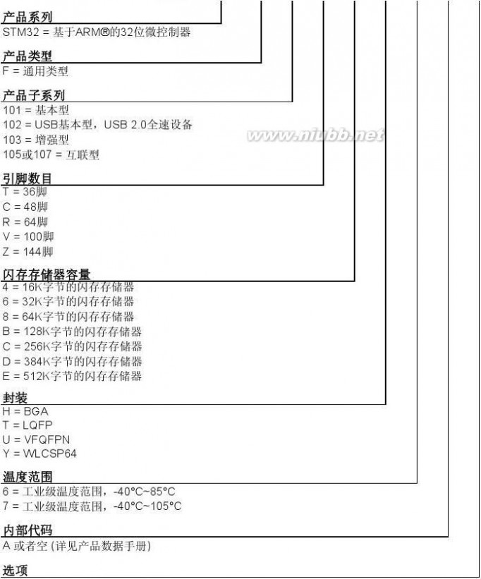

TR = 卷带式包装
参照2009年12月 RM0008 Reference Manual 英文第10版
本译文仅供参考,如有翻译错误,请以英文原稿为准。[www.61k.com]请读者随时注意在ST网站下载更新版本
stm32 STM32中文参考手册
STM32F10xxx参考手册
STM32
小容量STM32F101xx
小容量STM32F102xx
小容量STM32F103xx
中容量STM32F101xx
中容量STM32F102xx
中容量STM32F103xx
大容量STM32F101xx
大容量STM32F103xx
STM32F105xx
STM32F107xx
第1章:文中的缩写
●
●●●●●● ●●●● ● ●●● ●●● ●●
●●●●●● ●●●●● ●●●●●● ●●● ●●
●●●●●● ●●●● ● ●●● ● ●●● ●●
● ● ● ● ● ● ● ● ● ● ● ● ● ● ● ● ● ● ● ●
● ● ● ● ● ● ● ● ● ● ● ● ● ● ● ● ● ● ● ● ● ●
扩展:stm32中文参考手册 pdf / stm32中文参考手册 v10 / stm32的datebase
● ● ● ● ● ● ● ● ● ● ● ● ● ● ● ● ● ● ● ● ● ●
●●●●●● ●●●●●●●●●●●●●●●●●● ●●
●●●●● ●●●●●●●●●●●● ●●●●● ●●
●●●●● ●●●●●●●●●●●● ●●●●●●●●
第2章:存储器和总线构架●
第3章:CRC计算单元(CRC)第4章:电源控制(PWR)
●●
第5章:备份寄存器(BKP)
●
第6章:小容量、中容量和大容量产品的复位和时钟控制(RCC)第7章:互联型产品的复位和时钟控制(RCC)第8章:通用和复用功能I/O(GPIO和AFIO)第9章:中断和事件
● ●●
第10章:DMA控制器(DMA)
●
第11章:模拟/数字转换(ADC)第12章:数字/模拟转换(DAC)
●
第13章:高级控制定时器(TIM1和TIM8)第14章:通用定时器(TIMx)
●
第15章:基本定时器(TIM6和TIM7)第16章:实时时钟(RTC)
●
第17章:独立看门狗(IWDG)
●
第18章:窗口看门狗(WWDG)●
第19章:灵活的静态存储器控制器(FSMC)第20章:SDIO接口(SDIO)
第21章:USB全速设备接口(USB)第22章:控制器局域网(bxCAN)第23章:串行外设接口(SPI)第24章:I2C接口
●●
第25章:通用同步异步收发器(USART)第26章:USB OTG全速(OTG_FS)
●
第27章:以太网(ETH):具有DMA控制器的介质访问控制(MAC)第28章:器件电子签名
●
第29章:调试支持(DBG)
●
● 表示所在行对应的章节适用于该列标示的产品系列
提示:点击上表中的章节名字可以直接跳转到对应的章节。[www.61k.com]
参照2009年12月 RM0008 Reference Manual 英文第10版
本译文仅供参考,如有翻译错误,请以英文原稿为准。请读者随时注意在ST网站下载更新版本

stm32 STM32中文参考手册
STM32F10xxx参考手册
下表给出了一个交叉参考,在使用各功能模块时应重点阅读哪些章节:
功能模块
备份寄存器(BKP)
通用输入输出端口(GPIO)
通用串行总线(USB)
通用同步异步收发器(USART)
通用串行总线OTG(OTG_FS)
模拟/数字转换(ADC)
静态存储器控制器(FSMC)
独立看门狗(IWDG)
窗口看门狗WWDG)
控制器局域网(bxCAN)
数字/模拟转换(DAC)
定时器(TIMx(x=1…8))
串行外设总线(SPI)
以太网(ETH)
实时时钟(RTC)
芯片间总线接口(I2C)
SDIO接口(SDIO)
第1章:文中的缩写
●●●●●●●●●●● ● ● ● ●●●
第2章:存储器和总线构架●●●●●●●●●●● ● ● ● ●●●
第3章:CRC计算单元(CRC)第4章:电源控制(PWR)
●●●●●●●●●●● ● ● ● ●●●
第5章:备份寄存器(BKP)●◎
第6章:小容量、中容量和大容量产品的复位和时钟控制(RCC) 或
第7章:互联型产品的复位和时钟控制(RCC)第8章:通用和复用功能I/O(GPIO和AFIO)第9章:中断和事件
●●●●●●●●●●● ● ● ● ●●●◎●●●●◎●●●●● ● ● ● ●●●
◎◎◎◎◎
◎◎◎◎ ◎ ◎ ◎ ◎◎◎
◎◎
●
●●
●
●
●
●
●
●
●
◎ ◎ ◎ ●
●
●
●
●
第10章:DMA控制器(DMA)
◎◎◎
第11章:模拟/数字转换(ADC)第12章:数字/模拟转换(DAC)
●
第13章:高级控制定时器(TIM1和TIM8)第14章:通用定时器(TIMx)
◎◎
第15章:基本定时器(TIM6和TIM7)第16章:实时时钟(RTC)
◎◎●
●
第17章:独立看门狗(IWDG)
第18章:窗口看门狗(WWDG)
第19章:灵活的静态存储器控制器(FSMC)第20章:SDIO接口(SDIO)
第21章:USB全速设备接口(USB)第22章:控制器局域网(bxCAN)第23章:串行外设接口(SPI)第24章:I2C接口
第25章:通用同步异步收发器(USART)第26章:USB OTG全速(OTG_FS)
第27章:以太网(ETH):具有DMA控制器的介质访问控制(MAC)
第28章:器件电子签名
第29章:调试支持(DBG)
◎◎◎◎◎◎◎◎◎◎◎ ◎ ◎ ◎ ◎◎◎
● 表示对应的章节是必读的 ◎ 表示对应的章节是选读的
注:请区分第7章的内容只适合于互联型产品,第6章的内容适合于除互联型产品以外的产品。[www.61k.com]
参照2009年12月 RM0008 Reference Manual 英文第10版
本译文仅供参考,如有翻译错误,请以英文原稿为准。请读者随时注意在ST网站下载更新版本

(
stm32 STM32中文参考手册
STM32F10xxx参考手册

参考手册
STM32F101xx, STM32F102xx、STM32F103xx、STM32F105xx
和STM32F107xx,ARM内核32位高性能微控制器
导言
本参考手册针对应用开发,提供关于如何使用STM32F101xx、STM32F102xx、STM32F103和STM32F105xx/STM32F107xx微控制器的存储器和外设的详细信息。[www.61k.com]在本参考手册中STM32F101xx、STM32F102xx、STM32F103和STM32F105xx/STM32F107xx被统称为STM32F10xxx。
STM32F10xxx系列拥有不同的存储器容量、封装和外设配置。
关于订货编号、电气和物理性能参数,请参考小容量、中容量和大容量的STM32F101xx和STM32F103xx的数据手册,小容量和中容量的STM32F102xx数据手册和STM32F105xx/ STM32F107xx互联型产品的数据手册。
关于芯片内部闪存的编程,擦除和保护操作,请参考。
关于ARM Cortex?-M3内核的具体信息,请参考Cortex?-M3技术参考手册。
扩展:stm32中文参考手册 pdf / stm32中文参考手册 v10 / stm32的datebase
相关文档
● Cortex?-M3技术参考手册,可按下述链接下载: 下述文档可在ST网站下载(http://www.st.com/mcu/):
● STM32F101xx、STM32F102xx和STM32F103xx的数据手册。
● STM32F10xxx闪存编程手册。 相关数据手册下载地址:
小容量STM32F101xx:http://www.st.com/stonline/products/literature/ds/15058.pdf
中容量STM32F101xx:http://www.st.com/stonline/products/literature/ds/13586.pdf
大容量STM32F101xx:http://www.st.com/stonline/products/literature/ds/14610.pdf
小容量STM32F102xx:http://www.st.com/stonline/products/literature/ds/15057.pdf
中容量STM32F102xx:http://www.st.com/stonline/products/literature/ds/15056.pdf
小容量STM32F103xx:http://www.st.com/stonline/products/literature/ds/15060.pdf
中容量STM32F103xx:http://www.st.com/stonline/products/literature/ds/13587.pdf
大容量STM32F103xx:http://www.st.com/stonline/products/literature/ds/14611.pdf
互联型STM32F105xx/STM32F107xx:http://www.st.com/stonline/products/literature/ds/15274.pdf
STM32F10xxx Cortex-M3编程手册:
参照2009年12月 RM0008 Reference Manual 英文第10版

本译文仅供参考,如有翻译错误,请以英文原稿为准。请读者随时注意在ST网站下载更新版本
stm32 STM32中文参考手册
目录 STM32F10xxx参考手册
目录
1 文中的缩写 24
1.1 1.2 1.3
寄存器描述表中使用的缩写列表 24 术语表 可用的外设 系统构架 存储器组织 存储器映像 2.3.1
2.3.2 2.3.3 2.4
24 24 25 27 28
2 存储器和总线构架 25
2.1 2.2 2.3
嵌入式SRAM 29 位段 29 嵌入式闪存 30
33 34 34 34 35
启动配置 CRC简介 CRC主要特性 CRC功能描述 CRC寄存器 3.4.1 3.4.2 3.4.3 3.4.4
3 CRC计算单元(CRC) 34
3.1 3.2 3.3 3.4
4
数据寄存器(CRC_DR) 35 独立数据寄存器(CRC_IDR) 35 控制寄存器(CRC_CR) 36 CRC寄存器映像 36
电源控制(PWR) 37 4.1
电源 4.1.1 4.1.2 4.1.3 4.2
4.2.1 4.2.2 4.3
4.3.1 4.3.2 4.3.3 4.3.4 4.3.5 4.3.6 4.4
4.4.1 4.4.2 4.4.3
37
独立的A/D转换器供电和参考电压 37 电池备份区域 38 电压调节器 38
38
上电复位(POR)和掉电复位(PDR) 38 可编程电压监测器(PVD) 39
40
降低系统时钟 40 外部时钟的控制 40 睡眠模式 40 停止模式 41 待机模式 42 低功耗模式下的自动唤醒(AWU) 43
电源管理器
低功耗模式
电源控制寄存器 44
5
电源控制寄存器(PWR_CR) 44 电源控制/状态寄存器(PWR_CSR) 45 PWR寄存器地址映像 46
备份寄存器(BKP) 47 5.1 5.2
BKP简介 BKP特性
47 47 7/754

参照2009年12月 RM0008 Reference Manual 英文第10版
本译文仅供参考,如有翻译错误,请以英文原稿为准。(www.61k.com]请读者随时注意在ST网站下载更新版本
stm32 STM32中文参考手册
目录 STM32F10xxx参考手册
5.3 BKP功能描述
5.3.1
5.3.2
5.4
5.4.1
5.4.2
5.4.3
5.4.4
5.4.5 47 侵入检测 47 RTC校准 48 BKP寄存器描述 48
6 备份数据寄存器x(BKP_DRx) (x = 1 … 10) 48 RTC时钟校准寄存器(BKP_RTCCR) 48 备份控制寄存器(BKP_CR) 49 备份控制/状态寄存器(BKP_CSR) 49 BKP寄存器映像 51 小容量、中容量和大容量产品的复位和时钟控制(RCC) 54
6.1 复位
6.1.1
6.1.2
6.1.3
6.2 时钟
6.2.1
6.2.2
6.2.3
6.2.4
6.2.5
6.2.6
6.2.7
6.2.8
6.2.9
6.2.10
6.3
6.3.1
6.3.2
6.3.3
6.3.4
6.3.5
6.3.6
6.3.7
6.3.8
6.3.9
6.3.10
6.3.11 54 系统复位 54 电源复位 54 备份域复位 55 55 HSE时钟 57 HSI时钟 57 PLL 58 LSE时钟 58 LSI时钟 58 系统时钟(SYSCLK)选择 59 时钟安全系统(CSS) 59 RTC时钟 59 看门狗时钟 59 时钟输出 59 RCC寄存器描述 60
7 时钟控制寄存器(RCC_CR) 60 时钟配置寄存器(RCC_CFGR) 61 时钟中断寄存器 (RCC_CIR) 63 APB2外设复位寄存器 (RCC_APB2RSTR) 65 APB1外设复位寄存器 (RCC_APB1RSTR) 67 AHB外设时钟使能寄存器 (RCC_AHBENR) 69 APB2外设时钟使能寄存器(RCC_APB2ENR) 70 APB1外设时钟使能寄存器(RCC_APB1ENR) 71 备份域控制寄存器 (RCC_BDCR) 74 控制/状态寄存器 (RCC_CSR) 75 RCC寄存器地址映像 77 互联型产品的复位和时钟控制(RCC) 78
7.1 复位
7.1.1
7.1.2
7.1.3
7.2 时钟
7.2.1
7.2.2
7.2.3
7.2.4
7.2.5
7.2.6 78 系统复位 78 电源复位 78 备份域复位 79 79 HSE时钟 81 HSI时钟 82 PLL 82 LSE时钟 82 LSI时钟 83 系统时钟(SYSCLK)选择 83
8/754

参照2009年12月 RM0008 Reference Manual 英文第10版
本译文仅供参考,如有翻译错误,请以英文原稿为准。(www.61k.com]请读者随时注意在ST网站下载更新版本
stm32 STM32中文参考手册
目录 STM32F10xxx参考手册
7.2.7
7.2.8
7.2.9
7.2.10
7.3
7.3.1
7.3.2
7.3.3
7.3.4
7.3.5
7.3.6
7.3.7
7.3.8
7.3.9
7.3.10
7.3.11
7.3.12
扩展:stm32中文参考手册 pdf / stm32中文参考手册 v10 / stm32的datebase
7.3.13 时钟安全系统(CSS) 83 RTC时钟 83 看门狗时钟 84 时钟输出 84 85 RCC寄存器
8 时钟控制寄存器(RCC_CR) 85 时钟配置寄存器(RCC_CFGR) 86 时钟中断寄存器(RCC_CIR) 88 APB2外设复位寄存器(RCC_APB2RSTR) 91 APB1外设复位寄存器(RCC_APB1RSTR) 92 AHB外设时钟使能寄存器(RCC_AHBENR) 94 APB2外设时钟使能寄存器(RCC_APB2ENR) 95 APB1外设时钟使能寄存器(RCC_APB1ENR) 97 备份域控制寄存器(RCC_BDCR) 99 控制/状态寄存器(RCC_CSR) 100 AHB外设时钟复位寄存器(RCC_AHBRSTR) 101 时钟配置寄存器2(RCC_CFGR2) 101 RCC寄存器地址映像 103 通用和复用功能I/O(GPIO和AFIO) 105
8.1 GPIO功能描述
8.1.1
8.1.2
8.1.3
8.1.4
8.1.5
8.1.6
8.1.7
8.1.8
8.1.9
8.1.10
8.1.11
8.2
8.2.1
8.2.2
8.2.3
8.2.4
8.2.5
8.2.6
8.2.7
8.3
8.3.1
8.3.2
8.3.3
8.3.4
8.3.5
8.3.6
8.3.7
8.3.8
8.3.9
8.3.10 105 通用I/O(GPIO) 106 单独的位设置或位清除 107 外部中断/唤醒线 107 复用功能(AF) 107 软件重新映射I/O复用功能 107 GPIO锁定机制 107 输入配置 107 输出配置 108 复用功能配置 109 模拟输入配置 109 外设的GPIO配置 110 端口配置低寄存器(GPIOx_CRL) (x=A..E) 113 端口配置高寄存器(GPIOx_CRH) (x=A..E) 114 端口输入数据寄存器(GPIOx_IDR) (x=A..E) 114 端口输出数据寄存器(GPIOx_ODR) (x=A..E) 115 端口位设置/清除寄存器(GPIOx_BSRR) (x=A..E) 115 端口位清除寄存器(GPIOx_BRR) (x=A..E) 115 端口配置锁定寄存器(GPIOx_LCKR) (x=A..E) 116 把OSC32_IN/OSC32_OUT作为GPIO 端口PC14/PC15 116 把OSC_IN/OSC_OUT引脚作为GPIO端口PD0/PD1 117 CAN1复用功能重映射 117 CAN2复用功能重映射 117 JTAG/SWD复用功能重映射 117 ADC复用功能重映射 118 定时器复用功能重映射 118 USART复用功能重映射 119 I2C1复用功能重映射 120 SPI 1复用功能重映射 120
9/754

参照2009年12月 RM0008 Reference Manual 英文第10版
本译文仅供参考,如有翻译错误,请以英文原稿为准。(www.61k.com]请读者随时注意在ST网站下载更新版本 GPIO寄存器描述 113 复用功能I/O和调试配置(AFIO) 116
stm32 STM32中文参考手册
目录 STM32F10xxx参考手册
8.3.11
8.3.12
8.4
8.4.1
8.4.2
8.4.3
8.4.4
8.4.5
8.4.6
8.5 SPI3复用功能重映射 120 以太网复用功能重映射 121 事件控制寄存器(AFIO_EVCR) 121 复用重映射和调试I/O配置寄存器(AFIO_MAPR) 121 外部中断配置寄存器1(AFIO_EXTICR1) 126 外部中断配置寄存器2(AFIO_EXTICR2) 127 外部中断配置寄存器3(AFIO_EXTICR3) 127 外部中断配置寄存器4(AFIO_EXTICR4) 128 AFIO寄存器描述 121 GPIO 和AFIO寄存器地址映象 129
嵌套向量中断控制器 130
9.1.1
9.1.2 系统嘀嗒(SysTick)校准值寄存器 130 中断和异常向量 130
主要特性 134
框图 135
唤醒事件管理 135
功能说明 135
外部中断/事件线路映像 137 9 中断和事件 130 9.1 9.2 外部中断/事件控制器(EXTI) 134 9.2.1 9.2.2 9.2.3 9.2.4 9.2.5
9.3 EXTI 寄存器描述 138
9.3.1
9.3.2
9.3.3
9.3.4
9.3.5
9.3.6
9.3.7
10 中断屏蔽寄存器(EXTI_IMR) 138 事件屏蔽寄存器(EXTI_EMR) 138 上升沿触发选择寄存器(EXTI_RTSR) 139 下降沿触发选择寄存器(EXTI_FTSR) 139 软件中断事件寄存器(EXTI_SWIER) 140 挂起寄存器(EXTI_PR) 140 外部中断/事件寄存器映像 141 DMA控制器(DMA) 142
10.1
10.2
10.3 DMA简介 DMA主要特性 功能描述 142 142 143
10.3.1
10.3.2
10.3.3
10.3.4
10.3.5
10.3.6
10.3.7
10.4
10.4.1
10.4.2
10.4.3
10.4.4
10.4.5
10.4.6
10.4.7 DMA处理 143 仲裁器 144 DMA 通道 144 可编程的数据传输宽度、对齐方式和数据大小端 145 错误管理 146 中断 146 DMA请求映像 147 149 DMA寄存器
11 DMA中断状态寄存器(DMA_ISR) 149 DMA中断标志清除寄存器(DMA_IFCR) 150 DMA通道x配置寄存器(DMA_CCRx)(x = 1…7) 150 DMA通道x传输数量寄存器(DMA_CNDTRx)(x = 1…7) 152 DMA通道x外设地址寄存器(DMA_CPARx)(x = 1…7) 152 DMA通道x存储器地址寄存器(DMA_CMARx)(x = 1…7) 152 DMA寄存器映像 153 模拟/数字转换(ADC) 155
10/754

参照2009年12月 RM0008 Reference Manual 英文第10版
本译文仅供参考,如有翻译错误,请以英文原稿为准。[www.61k.com]请读者随时注意在ST网站下载更新版本
stm32 STM32中文参考手册
目录 STM32F10xxx参考手册
11.1 11.2 11.3
ADC介绍 ADC主要特征 ADC功能描述
155 155 156
11.3.1
11.3.2 11.3.3 11.3.4 11.3.5 11.3.6 11.3.7 11.3.8 11.3.9 11.3.10 11.4 11.5 11.6 11.7 11.8 11.9
校准
ADC开关控制 157 ADC时钟 157 通道选择 157 单次转换模式 157 连续转换模式 158 时序图 158 模拟看门狗 158 扫描模式 159 注入通道管理 159 间断模式 160
161 161 162 163 163
数据对齐 外部触发转换 DMA请求 双ADC模式
可编程的通道采样时间 161
11.9.1 11.9.2 11.9.3 11.9.4 11.9.5 11.9.6 11.9.7 11.9.8 11.9.9 同步注入模式 164 同步规则模式 165 快速交叉模式 165 慢速交叉模式 166 交替触发模式 166 独立模式 167 混合的规则/注入同步模式 167 混合的同步规则+交替触发模式 167 混合同步注入 + 交叉模式 168
168 169 170
扩展:stm32中文参考手册 pdf / stm32中文参考手册 v10 / stm32的datebase
11.10 温度传感器 11.11 ADC中断 11.12 ADC寄存器
11.12.1 11.12.2 11.12.3 11.12.4 11.12.5 11.12.6 11.12.7 11.12.8 11.12.9 11.12.10 11.12.11 11.12.12 11.12.13 11.12.14 11.12.15
12
ADC状态寄存器(ADC_SR) 170 ADC控制寄存器1(ADC_CR1) 171 ADC控制寄存器2(ADC_CR2) 173 ADC采样时间寄存器1(ADC_SMPR1) 175 ADC采样时间寄存器2(ADC_SMPR2) 175 ADC注入通道数据偏移寄存器x (ADC_JOFRx)(x=1..4) 176 ADC看门狗高阀值寄存器(ADC_HTR) 176 ADC看门狗低阀值寄存器(ADC_LRT) 176 ADC规则序列寄存器1(ADC_SQR1) 177 ADC规则序列寄存器2(ADC_SQR2) 177 ADC规则序列寄存器3(ADC_SQR3) 178 ADC注入序列寄存器(ADC_JSQR) 178 ADC 注入数据寄存器x (ADC_JDRx) (x= 1..4) 179 ADC规则数据寄存器(ADC_DR) 179 ADC寄存器地址映像 180
数字/模拟转换(DAC) 182 12.1
DAC简介
182 11/754

参照2009年12月 RM0008 Reference Manual 英文第10版
本译文仅供参考,如有翻译错误,请以英文原稿为准。(www.61k.com]请读者随时注意在ST网站下载更新版本
stm32 STM32中文参考手册
目录 STM32F10xxx参考手册
12.2
12.3 DAC主要特征 DAC功能描述 182 183
12.3.1
12.3.2
12.3.3
12.3.4
12.3.5
12.3.6
12.3.7
12.3.8
12.3.9
12.4
12.4.1
12.4.2
12.4.3
12.4.4
12.4.5
12.4.6
12.4.7
12.4.8
12.4.9
12.4.10
12.4.11
12.5
12.5.1
12.5.2
12.5.3
12.5.4
12.5.5
12.5.6
12.5.7
12.5.8
12.5.9
12.5.10
12.5.11
12.5.12
12.5.13
12.5.14 使能DAC通道 183 使能DAC输出缓存 184 DAC数据格式 184 DAC转换 185 DAC输出电压 185 选择DAC触发 185 DMA请求 186 噪声生成 186 三角波生成 187 不使用波形发生器的独立触发 187 使用相同LFSR的独立触发 188 使用不同LFSR的独立触发 188 产生相同三角波的独立触发 188 产生不同三角波的独立触发 188 同时软件启动 189 不使用波形发生器的同时触发 189 使用相同LFSR的同时触发 189 使用不同LFSR的同时触发 189 使用相同三角波发生器的同时触发 189 使用不同三角波发生器的同时触发 190 191 双DAC通道转换 187 DAC寄存器
13 DAC控制寄存器(DAC_CR) 191 DAC软件触发寄存器(DAC_SWTRIGR) 193 DAC通道1的12位右对齐数据保持寄存器(DAC_DHR12R1) 194 DAC通道1的12位左对齐数据保持寄存器(DAC_DHR12L1) 194 DAC通道1的8位右对齐数据保持寄存器(DAC_DHR8R1) 194 DAC通道2的12位右对齐数据保持寄存器(DAC_DHR12R2) 195 DAC通道2的12位左对齐数据保持寄存器(DAC_DHR12L2) 195 DAC通道2的8位右对齐数据保持寄存器(DAC_DHR8R2) 195 双DAC的12位右对齐数据保持寄存器(DAC_DHR12RD) 196 双DAC的12位左对齐数据保持寄存器(DAC_DHR12LD) 196 双DAC的8位右对齐数据保持寄存器(DAC_DHR8RD) 196 DAC通道1数据输出寄存器(DAC_DOR1) 197 DAC通道2数据输出寄存器(DAC_DOR2) 197 DAC寄存器映像 198 高级控制定时器(TIM1和TIM8) 199
13.1
13.2
13.3 TIM1和TIM8简介 199 TIM1和TIM8主要特性 199 TIM1和TIM8功能描述 200
时基单元 200
计数器模式 202
重复计数器 209
时钟选择 210
捕获/比较通道 213
输入捕获模式 215
PWM输入模式 216
强置输出模式 216
12/754

参照2009年12月 RM0008 Reference Manual 英文第10版
本译文仅供参考,如有翻译错误,请以英文原稿为准。[www.61k.com]请读者随时注意在ST网站下载更新版本 13.3.1 13.3.2 13.3.3 13.3.4 13.3.5 13.3.6 13.3.7 13.3.8
stm32 STM32中文参考手册
目录 STM32F10xxx参考手册
13.3.9
13.3.10
13.3.11
13.3.12
13.3.13
13.3.14
13.3.15
13.3.16
13.3.17
13.3.18
13.3.19
13.3.20
13.3.21
13.4
13.4.1
13.4.2
13.4.3
13.4.4
13.4.5
13.4.6
13.4.7
13.4.8
13.4.9
13.4.10
13.4.11
13.4.12
13.4.13
13.4.14
13.4.15
13.4.16
13.4.17
13.4.18
13.4.19
13.4.20
13.4.21 输出比较模式 217 PWM模式 218 互补输出和死区插入 220 使用刹车功能 221 在外部事件时清除OCxREF信号 223 产生六步PWM输出 223 单脉冲模式 224 编码器接口模式 225 定时器输入异或功能 227 与霍尔传感器的接口 227 TIMx定时器和外部触发的同步 229 定时器同步 232 调试模式 232 TIM1和TIM8寄存器描述 233
14 TIM1和TIM8控制寄存器1(TIMx_CR1) 233 TIM1和TIM8控制寄存器2(TIMx_CR2) 234 TIM1和TIM8从模式控制寄存器(TIMx_SMCR) 235 TIM1和TIM8 DMA/中断使能寄存器(TIMx_DIER) 237 TIM1和TIM8状态寄存器(TIMx_SR) 238 TIM1和TIM8事件产生寄存器(TIMx_EGR) 239 TIM1和TIM8捕获/比较模式寄存器1(TIMx_CCMR1) 240 TIM1和TIM8捕获/比较模式寄存器2(TIMx_CCMR2) 242 TIM1和TIM8捕获/比较使能寄存器(TIMx_CCER) 244 TIM1和TIM8计数器(TIMx_CNT) 246 TIM1和TIM8预分频器(TIMx_PSC) 246 TIM1和TIM8自动重装载寄存器(TIMx_ARR) 246 TIM1和TIM8重复计数寄存器(TIMx_RCR) 246 TIM1和TIM8捕获/比较寄存器1(TIMx_CCR1) 247 TIM1和TIM8捕获/比较寄存器2(TIMx_CCR2) 247 TIM1和TIM8捕获/比较寄存器3(TIMx_CCR3) 247 TIM1和TIM8捕获/比较寄存器(TIMx_CCR4) 248 TIM1和TIM8刹车和死区寄存器(TIMx_BDTR) 248 TIM1和TIM8 DMA控制寄存器(TIMx_DCR) 249 TIM1和TIM8连续模式的DMA地址(TIMx_DMAR) 250 TIM1和TIM8寄存器图 251 通用定时器(TIMx) 253
扩展:stm32中文参考手册 pdf / stm32中文参考手册 v10 / stm32的datebase
14.1
14.2
14.3 TIMx简介 TIMx主要功能 TIMx功能描述 253 253 254
14.3.1
14.3.2
14.3.3
14.3.4
14.3.5
14.3.6
14.3.7
14.3.8
14.3.9
14.3.10
14.3.11
14.3.12 时基单元 254 计数器模式 255 时钟选择 263 捕获/比较通道 265 输入捕获模式 267 PWM输入模式 267 强置输出模式 268 输出比较模式 268 PWM 模式 269 单脉冲模式 271 在外部事件时清除OCxREF信号 273 编码器接口模式 273
13/754

参照2009年12月 RM0008 Reference Manual 英文第10版
本译文仅供参考,如有翻译错误,请以英文原稿为准。(www.61k.com)请读者随时注意在ST网站下载更新版本
stm32 STM32中文参考手册
目录 STM32F10xxx参考手册
14.3.13
14.3.14
14.3.15
14.3.16
14.4
14.4.1
14.4.2
14.4.3
14.4.4
14.4.5
14.4.6
14.4.7
14.4.8
14.4.9
14.4.10
14.4.11
14.4.12
14.4.13
14.4.14
14.4.15
14.4.16
14.4.17
14.4.18
14.4.19 定时器输入异或功能 275 定时器和外部触发的同步 275 定时器同步 277 调试模式 281 TIMx寄存器描述 282
15 控制寄存器1(TIMx_CR1) 282 控制寄存器2(TIMx_CR2) 283 从模式控制寄存器(TIMx_SMCR) 284 DMA/中断使能寄存器(TIMx_DIER) 285 状态寄存器(TIMx_SR) 286 事件产生寄存器(TIMx_EGR) 287 捕获/比较模式寄存器1(TIMx_CCMR1) 288 捕获/比较模式寄存器2(TIMx_CCMR2) 290 捕获/比较使能寄存器(TIMx_CCER) 292 计数器(TIMx_CNT) 293 预分频器(TIMx_PSC) 293 自动重装载寄存器(TIMx_ARR) 293 捕获/比较寄存器1(TIMx_CCR1) 293 捕获/比较寄存器2(TIMx_CCR2) 294 捕获/比较寄存器3(TIMx_CCR3) 294 捕获/比较寄存器4(TIMx_CCR4) 294 DMA控制寄存器(TIMx_DCR) 295 连续模式的DMA地址(TIMx_DMAR) 295 TIMx寄存器图 296 基本定时器(TIM6和TIM7) 298
15.1
15.2
15.3 TIM6和TIM7简介 298 TIM6和TIM7的主要特性 298 TIM6和TIM7的功能 299
时基单元 299
计数模式 300
时钟源 302
调试模式 303 15.3.1 15.3.2 15.3.3 15.3.4
15.4
15.4.1
15.4.2
15.4.3
15.4.4
15.4.5
15.4.6
15.4.7
15.4.8
15.4.9 TIM6和TIM7寄存器 303
16 TIM6和TIM7控制寄存器1(TIMx_CR1) 303 TIM6和TIM7控制寄存器2(TIMx_CR2) 304 TIM6和TIM7 DMA/中断使能寄存器(TIMx_DIER) 304 TIM6和TIM7状态寄存器(TIMx_SR) 305 TIM6和TIM7事件产生寄存器(TIMx_EGR) 305 TIM6和TIM7计数器(TIMx_CNT) 305 TIM6和TIM7预分频器(TIMx_PSC) 306 TIM6和TIM7自动重装载寄存器(TIMx_ARR) 306 TIM6和TIM7寄存器图 307 实时时钟(RTC) 308
16.1
16.2
16.3 RTC简介 主要特性 功能描述 308 308 308
16.3.1
16.3.2
16.3.3 概述 308 复位过程 309 读RTC寄存器 309
14/754

参照2009年12月 RM0008 Reference Manual 英文第10版
本译文仅供参考,如有翻译错误,请以英文原稿为准。[www.61k.com]请读者随时注意在ST网站下载更新版本
stm32 STM32中文参考手册
目录 STM32F10xxx参考手册
16.3.4
16.3.5
16.4
16.4.1
16.4.2
16.4.3
16.4.4
16.4.5
16.4.6
16.4.7 配置RTC寄存器 310 RTC标志的设置 310 RTC寄存器描述 311
17 RTC控制寄存器高位(RTC_CRH) 311 RTC控制寄存器低位(RTC_CRL) 311 RTC预分频装载寄存器(RTC_PRLH/RTC_PRLL) 312 RTC预分频器余数寄存器(RTC_DIVH / RTC_DIVL) 313 RTC计数器寄存器 (RTC_CNTH / RTC_CNTL) 313 RTC闹钟寄存器(RTC_ALRH/RTC_ALRL) 314 RTC寄存器映像 315 独立看门狗(IWDG) 316
17.1
17.2
17.3 简介 IWDG主要性能 IWDG功能描述 316 316 316
17.3.1
17.3.2
17.3.3
17.4
17.4.1
17.4.2
17.4.3
17.4.4
17.4.5 硬件看门狗 316 寄存器访问保护 316 调试模式 316 IWDG寄存器描述 317
18 键寄存器(IWDG_KR) 317 预分频寄存器(IWDG_PR) 318 重装载寄存器(IWDG_RLR) 318 状态寄存器(IWDG_SR) 319 IWDG寄存器映像 319 窗口看门狗(WWDG) 320
18.1
18.2
18.3
18.4
18.5
18.6 WWDG简介 320 WWDG主要特性 320 WWDG功能描述 320 如何编写看门狗超时程序 321 调试模式 寄存器描述 322 322 19 控制寄存器(WWDG_CR) 322 配置寄存器(WWDG_CFR) 322 状态寄存器(WWDG_SR) 323 WWDG寄存器映像 323 灵活的静态存储器控制器(FSMC) 324
19.1
19.2
19.3
19.4 FSMC功能描述 框图 AHB接口 324 324 325 支持的存储器和操作 325
NOR和PSRAM地址映像 327
NAND和PC卡地址映像 327
外部存储器接口信号 329
支持的存储器及其操作 330
时序规则 330
NOR闪存和PSRAM控制器时序图 330
15/754

参照2009年12月 RM0008 Reference Manual 英文第10版
本译文仅供参考,如有翻译错误,请以英文原稿为准。[www.61k.com)请读者随时注意在ST网站下载更新版本 18.6.1 18.6.2 18.6.3 18.6.4 19.3.1 19.4.1 19.4.2 19.5 19.5.1 19.5.2 19.5.3 19.5.4 外部设备地址映像 326 NOR闪存和PSRAM控制器 328
stm32 STM32中文参考手册
目录 STM32F10xxx参考手册
19.5.5
19.5.6
19.6
19.6.1
19.6.2
扩展:stm32中文参考手册 pdf / stm32中文参考手册 v10 / stm32的datebase
19.6.3
19.6.4
19.6.5
19.6.6
19.6.7
19.7 同步的成组读 343 NOR闪存和PSRAM控制器寄存器 347 外部存储器接口信号 352 NAND闪存/PC卡支持的存储器及其操作 353 NAND闪存、ATA和PC卡时序图 353 NAND闪存操作 354 NAND闪存预等待功能 355 NAND闪存的纠错码ECC计算(NAND闪存) 356 NAND闪存和PC卡控制器寄存器 356 NAND闪存和PC卡控制器 352 FSMC寄存器地址映象 362
SDIO主要功能
SDIO总线拓扑
SDIO功能描述 363 363 366 20 SDIO接口(SDIO) 363 20.1 20.2 20.3
20.3.1
20.3.2
20.4
20.4.1
20.4.2
20.4.3
20.4.4
20.4.5
20.4.6
20.4.7
20.4.8
20.4.9
20.4.10
20.4.11
20.4.12
20.4.13
20.4.14
20.5
20.5.1
20.5.2
20.5.3
20.5.4
20.5.5
20.5.6
20.5.7
20.5.8
20.6
20.6.1
20.6.2
20.6.3
20.6.4
20.7
20.7.1
20.7.2 SDIO适配器 367 SDIO AHB接口 374 374 卡识别模式 374 卡复位 374 操作电压范围确认 375 卡识别过程 375 写数据块 376 读数据块 376 数据流操作,数据流写入和数据流读出(只适用于多媒体卡) 376 擦除:成组擦除和扇区擦除 377 宽总线选择和解除选择 378 保护管理 378 卡状态寄存器 380 SD状态寄存器 382 SD的I/O模式 385 命令与响应 385 388 R1(普通响应命令) 388 R1b 388 R2(CID、CSD寄存器) 388 R3(OCR寄存器) 389 R4(快速I/O) 389 R4b 389 R5(中断请求) 390 R6(中断请求) 390 使用SDIO_D2信号线的SDIO I/O读等待操作 390 使用停止SDIO_CK的SDIO读等待操作 391 SDIO暂停/恢复操作 391 SDIO中断 391 命令完成指示关闭 391 命令完成指示使能 391
16/754

参照2009年12月 RM0008 Reference Manual 英文第10版
本译文仅供参考,如有翻译错误,请以英文原稿为准。[www.61k.com]请读者随时注意在ST网站下载更新版本 卡功能描述 响应格式 SDIO I/O卡特定的操作 390 CE-ATA特定操作 391
stm32 STM32中文参考手册
目录 STM32F10xxx参考手册
20.7.3
20.7.4
20.8
20.9 CE-ATA中断 392 中止CMD61 392 392 392 硬件流控制 SDIO寄存器
21 SDIO电源控制寄存器(SDIO_POWER) 392 SDIO时钟控制寄存器(SDIO_CLKCR) 392 SDIO参数寄存器(SDIO_ARG) 393 SDIO命令寄存器(SDIO_CMD) 393 SDIO命令响应寄存器(SDIO_RESPCMD) 394 SDIO响应1..4寄存器(SDIO_RESPx) 395 SDIO数据定时器寄存器(SDIO_DTIMER) 395 SDIO数据长度寄存器(SDIO_DLEN) 395 SDIO数据控制寄存器(SDIO_DCTRL) 396 SDIO数据计数器寄存器(SDIO_DCOUNT) 397 SDIO状态寄存器(SDIO_STA) 397 SDIO清除中断寄存器(SDIO_ICR) 398 SDIO中断屏蔽寄存器(SDIO_MASK) 399 SDIO FIFO计数器寄存器(SDIO_FIFOCNT) 401 SDIO数据FIFO寄存器(SDIO_FIFO) 401 SDIO寄存器映像 402 USB全速设备接口(USB) 403
21.1
21.2
21.3
21.4 USB简介 USB主要特征 USB功能描述 403 403 404 20.9.1 20.9.2 20.9.3 20.9.4 20.9.5 20.9.6 20.9.7 20.9.8 20.9.9 20.9.10 20.9.11 20.9.12 20.9.13 20.9.14 20.9.15 20.9.16 21.3.1
21.4.1
21.4.2
21.4.3
21.4.4
21.4.5
21.5
21.5.1
21.5.2
21.5.3
21.5.4 USB功能模块描述 405 通用USB设备编程 406 系统复位和上电复位 406 双缓冲端点 409 同步传输 410 挂起/恢复事件 411 编程中需要考虑的问题 406 USB寄存器描述 412
22 通用寄存器 412 端点寄存器 416 缓冲区描述表 419 USB寄存器映像 421 控制器局域网(bxCAN) 423
22.1
22.2
22.3 bxCAN简介 423 bxCAN主要特点 423 bxCAN总体描述 424
CAN 2.0B主动内核 424
控制、状态和配置寄存器 424
发送邮箱 424
接收过滤器 424
初始化模式 426
正常模式 426
睡眠模式(低功耗) 426
17/754

参照2009年12月 RM0008 Reference Manual 英文第10版
本译文仅供参考,如有翻译错误,请以英文原稿为准。(www.61k.com]请读者随时注意在ST网站下载更新版本 22.3.1 22.3.2 22.3.3 22.3.4 22.4 22.4.1 22.4.2 22.4.3 bxCAN工作模式 426
stm32 STM32中文参考手册
目录 STM32F10xxx参考手册
22.5 测试模式 427
22.5.1
22.5.2
22.5.3
22.6
22.7 静默模式 427 环回模式 427 环回静默模式 428 STM32F10xxx处于调试模式时 428 bxCAN功能描述 428
发送处理 428
时间触发通信模式 430
接收管理 430
标识符过滤 431
报文存储 434
出错管理 435
位时间特性 436
438 22.7.1 22.7.2 22.7.3 22.7.4 22.7.5 22.7.6 22.7.7 22.8
22.9 bxCAN中断 CAN 寄存器描述 439 23 寄存器访问保护 439 CAN控制和状态寄存器 439 CAN邮箱寄存器 447 CAN过滤器寄存器 451 bxCAN寄存器列表 454 串行外设接口(SPI) 457
23.1
23.2 SPI简介
SPI特征
I2S功能 457 457 458
459 SPI和I2S主要特征 457 22.9.1 22.9.2 22.9.3 22.9.4 22.9.5 23.2.1 23.2.2 23.3
23.3.1
23.3.2
23.3.3
23.3.4
23.3.5
23.3.6
23.3.7
23.3.8
23.3.9
23.3.10
23.3.11
23.4
23.4.1
23.4.2
23.4.3
23.4.4
23.4.5
23.4.6
23.4.7
23.4.8
23.4.9
23.5 SPI功能描述 概述 459 配置SPI为从模式 462 配置SPI为主模式 462 配置SPI为单工通信 463 数据发送与接收过程 463 CRC计算 468 状态标志 469 关闭SPI 470 利用DMA的SPI通信 470 错误标志 472 SPI中断 472 473 I2S功能描述 473 支持的音频协议 474 时钟发生器 479 I2S主模式 482 I2S从模式 483 状态标志位 484 错误标志位 485 I2S中断 485 DMA功能 485 I2S功能描述 SPI和I2S寄存器描述 486
扩展:stm32中文参考手册 pdf / stm32中文参考手册 v10 / stm32的datebase
18/754

参照2009年12月 RM0008 Reference Manual 英文第10版
本译文仅供参考,如有翻译错误,请以英文原稿为准。(www.61k.com]请读者随时注意在ST网站下载更新版本
stm32 STM32中文参考手册
目录 STM32F10xxx参考手册
23.5.1
23.5.2
23.5.3
23.5.4
23.5.5
23.5.6
23.5.7
23.5.8
23.5.9
23.5.10 SPI控制寄存器1(SPI_CR1)(I2S模式下不使用) 486 SPI控制寄存器2(SPI_CR2) 487 SPI 状态寄存器(SPI_SR) 488 SPI 数据寄存器(SPI_DR) 489 SPI CRC多项式寄存器(SPI_CRCPR)(I2S模式下不使用) 489 SPI Rx CRC寄存器(SPI_RXCRCR)(I2S模式下不使用) 490 SPI Tx CRC寄存器(SPI_TXCRCR) 490 SPI_I2S配置寄存器(SPI_I2S_CFGR) 490 SPI_I2S预分频寄存器(SPI_I2SPR) 491 SPI 寄存器地址映象 492
493
493
493
494 24 I2C接口 24.1 24.2 24.3 I2C简介 I2C主要特点 I2C功能描述
24.3.1
24.3.2
24.3.3
24.3.4
24.3.5
24.3.6
24.3.7
24.3.8
24.4
24.5
24.6 模式选择 494 I2C从模式 495 I2C主模式 497 错误条件 499 SDA/SCL线控制 500 SMBus 501 DMA请求 502 包错误校验(PEC) 503 504 505 505 I2C中断请求 I2C调试模式 I2C寄存器描述
25 控制寄存器1(I2C_CR1) 505 控制寄存器2(I2C_CR2) 507 自身地址寄存器1(I2C_OAR1) 508 自身地址寄存器2(I2C_OAR2) 509 数据寄存器(I2C_DR) 509 状态寄存器1(I2C_SR1) 510 状态寄存器2 (I2C_SR2) 512 时钟控制寄存器(I2C_CCR) 513 TRISE寄存器(I2C_TRISE) 514 I2C寄存器地址映象 515 通用同步异步收发器(USART) 516
25.1
25.2
25.3 USART介绍 516 USART主要特性 516 USART功能概述 517
USART 特性描述 518
发送器 519
接收器 521
分数波特率的产生 524
USART接收器容忍时钟的变化 525
多处理器通信 526
校验控制 527
LIN(局域互联网)模式 528
USART 同步模式 530
单线半双工通信 532
19/754

参照2009年12月 RM0008 Reference Manual 英文第10版
本译文仅供参考,如有翻译错误,请以英文原稿为准。[www.61k.com]请读者随时注意在ST网站下载更新版本 24.6.1 24.6.2 24.6.3 24.6.4 24.6.5 24.6.6 24.6.7 24.6.8 24.6.9 24.6.10 25.3.1 25.3.2 25.3.3 25.3.4 25.3.5 25.3.6 25.3.7 25.3.8 25.3.9 25.3.10
stm32 STM32中文参考手册
目录 STM32F10xxx参考手册
25.3.11
25.3.12
25.3.13
25.3.14
25.4
25.5
25.6 智能卡 532 IrDA SIR ENDEC 功能模块 533 利用DMA连续通信 535 硬件流控制 537 USART中断请求 538 USART模式配置 539 USART寄存器描述 540 26 状态寄存器(USART_SR) 540 数据寄存器(USART_DR) 541 波特比率寄存器(USART_BRR) 542 控制寄存器1(USART_CR1) 542 控制寄存器2(USART_CR2) 544 控制寄存器3(USART_CR3) 545 保护时间和预分频寄存器(USART_GTPR) 546 USART寄存器地址映象 548 USB OTG全速(OTG_FS) 549
26.1
26.2 OTG模块介绍 549 OTG_FS主要功能 549
通用功能 549
主机模式功能 550
设备模式功能 550
OTG全速控制器 551
全速OTG PHY(物理接口) 551
ID信号检测 552
HNP双角色设备 552
SRP双角色设备 553
553
具备SRP功能的设备 553
设备状态 554
设备端点 554
556
具备SRP功能的主机 556
USB主机状态 557
主机通道 558
主机调度器 558
560
主机SOF 560
设备SOF 560
560
562 25.6.1 25.6.2 25.6.3 25.6.4 25.6.5 25.6.6 25.6.7 25.6.8 26.2.1 26.2.2 26.2.3 26.3 26.3.1 26.3.2 26.4 26.4.1 26.4.2 26.4.3 26.5 26.5.1 26.5.2 26.5.3 26.6 26.6.1 26.6.2 26.6.3 26.6.4 26.7 26.7.1 26.7.2 26.8 26.9 OTG_FS功能描述 551 OTG双角色设备(DRD) 552 USB设备模式 USB主机 SOF触发 供电选项 USB数据FIFO
26.10 设备模式下的FIFO结构 563
26.10.1
26.10.2
26.11.1 设备模式下的接收FIFO 563 设备模式下的发送FIFO 563 主机模式下的接收FIFO 564
20/754

参照2009年12月 RM0008 Reference Manual 英文第10版
本译文仅供参考,如有翻译错误,请以英文原稿为准。[www.61k.com]请读者随时注意在ST网站下载更新版本 26.11 主机模式下的FIFO结构 564
stm32 STM32中文参考手册
目录 STM32F10xxx参考手册
26.11.2 主机模式下的发送FIFO 564
565
566 26.12 USB系统性能 26.13 OTG_FS中断
26.14.1
26.14.2
26.14.3
26.14.4
26.14.5
26.14.6
26.15.1
26.15.2
26.15.3
26.15.4
26.15.5
26.15.6
26.15.7
26.15.8 26.14 OTG_FS控制和状态寄存器 566 CSR存储器映像 567 OTG_FS全局寄存器 570 主机模式下的寄存器 585 设备模式下的寄存器 593 OTG_FS电源和时钟门控寄存器(OTG_FS_PCGCCTL) 608 OTG_FS寄存器映像 610 26.15 OTG_FS编程规则 617 控制器初始化 617 主机模式下的初始化 617 设备模式下的初始化 617 主机模式下的编程规则 618 设备模式下的编程规则 632 操作流程 633 最差情况下的响应时间 646 OTG编程规则 648 以太网(ETH):具有DMA控制器的介质访问控制(MAC) 652 27.1
27.2 以太网模块介绍 652 以太网模块主要功能 652
MAC控制器功能 652
DMA功能 653
PTP功能 654 27 27.2.1 27.2.2 27.2.3
扩展:stm32中文参考手册 pdf / stm32中文参考手册 v10 / stm32的datebase
27.3
27.4 以太网模块引脚和内部信号 654 以太网模块功能描述:SMI、MII和RMII 655
站点管理接口(SMI) 655
独立于介质的接口:MII 657
精简的独立于介质的接口:RMII 659
MII/RMII的选择 660
MAC 802.3帧格式 661
MAC帧的传输 663
MAC帧的接收 669
MAC中断 673
MAC过滤 673
MAC自循环模式 675
MAC管理计数器:MMC 675
电源管理:PMT 676
精确时间协议(IEEE1588 PTP) 678
使用DMA发送的初始化步骤 683
主机总线突发访问 683
主机数据缓存对齐 684
缓冲区大小计算 684
DMA仲裁器 684
DMA错误响应 684
21/754

参照2009年12月 RM0008 Reference Manual 英文第10版
本译文仅供参考,如有翻译错误,请以英文原稿为准。[www.61k.com]请读者随时注意在ST网站下载更新版本 27.4.1 27.4.2 27.4.3 27.4.4 27.5 27.5.1 27.5.2 27.5.3 27.5.4 27.5.5 27.5.6 27.5.7 27.5.8 27.5.9 27.6 27.6.1 27.6.2 27.6.3 27.6.4 27.6.5 27.6.6 以太网模块功能描述:MAC 802.3 660 以太网功能描述:DMA控制器操作 682
stm32 STM32中文参考手册
目录 STM32F10xxx参考手册
27.6.7
27.6.8
27.6.9
27.7
27.8 发送DMA设置 684 接收DMA设置 694 DMA中断 700 701 以太网中断 以太网寄存器描述 702 28 MAC寄存器描述 702 MMC寄存器描述 713 IEEE 1588时间戳寄存器 716 DMA寄存器描述 719 以太网寄存器映像 729 器件电子签名 732
28.1
28.2 存储器容量寄存器 732 闪存容量寄存器 732 产品唯一身份标识寄存器(96位) 732
概况
ARM参考文献 734 735 28.1.1 27.8.1 27.8.2 27.8.3 27.8.4 27.8.5 29 调试支持(DBG) 734 29.1 29.2
29.3
29.4 SWJ调试端口(serial wire and JTAG) 735 JTAG-DP和SW-DP切换的机制 736
SWJ调试端口脚 736
灵活的SWJ-DP脚分配 736
JTAG脚上的内部上拉和下拉 737
利用串行接口并释放不用的调试脚作为普通I/O口 737 引脚分布和调试端口脚 736 29.3.1 29.4.1 29.4.2 29.4.3 29.4.4
29.5
29.6 STM32F10xxx JTAG TAP 连接 738 ID 代码和锁定机制 738
微控制器设备ID编码 738
边界扫描TAP 739
Cortex-M3 TAP 740
Cortex-M3 JEDEC-106 ID代码 740
740
741 29.6.1 29.6.2 29.6.3 29.6.4 29.7 29.8 JTAG调试端口 SW调试端口
29.8.1
29.8.2
29.8.3
29.8.4
29.8.5
29.8.6
29.9 SW协议介绍 741 SW协议序列 741 SW-DP状态机(Reset, idle states, ID code) 742 DP和AP读/写访问 742 SW-DP寄存器 742 SW-AP寄存器 743
744 对于JTAG-DP或SWDP都有效的AHB-AP (AHB 访问端口) 743 29.10 内核调试
29.11 调试器主机在系统复位下的连接能力 744 29.12 FPB (Flash patch breakpoint) 744 29.13 DWT(数据观察点触发data watchpoint trigger) 745 29.14 ITM (指令跟踪微单元 instrumentation trace macrocell) 745
29.14.1
29.14.2 概述 745 时间戳包,同步和溢出包 745
22/754

参照2009年12月 RM0008 Reference Manual 英文第10版
本译文仅供参考,如有翻译错误,请以英文原稿为准。[www.61k.com]请读者随时注意在ST网站下载更新版本
stm32 STM32中文参考手册
目录 STM32F10xxx参考手册
29.15 ETM模块(嵌入式跟踪微单元Embedded Trace Macrocell) 746
29.15.1
29.15.2
29.15.3
29.15.4
29.16.1
29.16.2
29.16.3
29.17.1
29.17.2
29.17.3
29.17.4
29.17.5
29.17.6
29.17.7
29.17.8
29.17.9
29.17.10
概述 746 信号协议和包类型 746 主要的ETM寄存器 747 配置实例 747 低功耗模式的调试支持 747 支持定时器、看门狗、bxCAN和I2C的调试 747 调试MCU配置寄存器 748 导言 750 跟踪引脚分配 750 TPUI格式器 752 TPUI帧异步包 752 同步帧包的发送 752 同步模式 752 异步模式 753 TRACECLKIN在STM32F10xxx内部的连接 753 TPIU寄存器 753 配置的例子 754 29.16 MCU调试模块(MCUDBG) 747 29.17 TPIU (跟踪端口接口单元 Trace Port Interface Unit) 750 29.18 DBG寄存器地址映象 754
23/754
参照2009年12月 RM0008 Reference Manual 英文第10版
本译文仅供参考,如有翻译错误,请以英文原稿为准。[www.61k.com)请读者随时注意在ST网站下载更新版本

stm32 STM32中文参考手册
存储器和总线架构 STM32F10xxx参考手册 1
1.1 文中的缩写 寄存器描述表中使用的缩写列表
在对寄存器的描述中使用了下列缩写: read / write (rw)
read-only (r)
write-only (w)
read/clear (rc_w1)
read / clear (rc_w0)
read / clear by read (rc_r)
read / set (rs)
read-only write trigger (rt_w)
toggle (t)
Reserved(Res.) 软件能读写此位。(www.61k.com] 软件只能读此位。 软件只能写此位,读此位将返回复位值。 软件可以读此位,也可以通过写’1’清除此位,写’0’对此位无影响。 软件可以读此位,也可以通过写’0’清除此位,写’1’对此位无影响。 软件可以读此位;读此位将自动地清除它为’0’,写’0’对此位无影响。 软件可以读也可以设置此位,写’0’对此位无影响。 软件可以读此位;写’0’或’1’触发一个事件但对此位数值没有影响。

扩展:stm32中文参考手册 pdf / stm32中文参考手册 v10 / stm32的datebase
软件只能通过写’1’来翻转此位,写’0’对此位无影响。 保留位,必须保持默认值不变
1.2 术语表
● 小容量产品是指闪存存储器容量在16K至32K字节之间的STM32F101xx、STM32F102xx和
STM32F103xx微控制器。
● 中容量产品是指闪存存储器容量在64K至128K字节之间的STM32F101xx、STM32F102xx
和STM32F103xx微控制器。
● 大容量产品是指闪存存储器容量在256K至512K字节之间的STM32F101xx和STM32F103xx
微控制器。
● 互联型产品是STM32F105xx和STM32F107xx微控制器。
1.3 可用的外设
有关STM32微控制器系列全部型号中,某外设存在与否及其数目,请查阅相应的小容量、中容量或者大容量STM32F101xx和STM32F103xx以及小容量和中容量STM32F102xx的数据手册,以及STM32F105xx/STM32F107xx数据手册。
24/754
参照2009年12月 RM0008 Reference Manual 英文第10版
本译文仅供参考,如有翻译错误,请以英文原稿为准。请读者随时注意在ST网站下载更新版本
stm32 STM32中文参考手册
存储器和总线架构

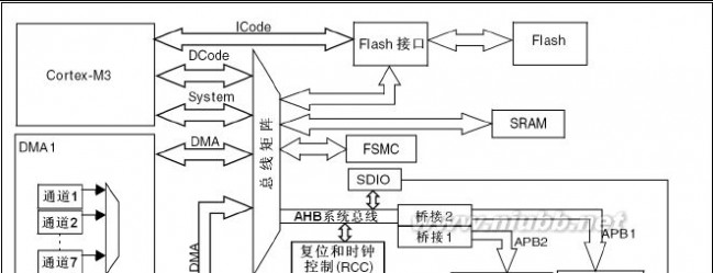
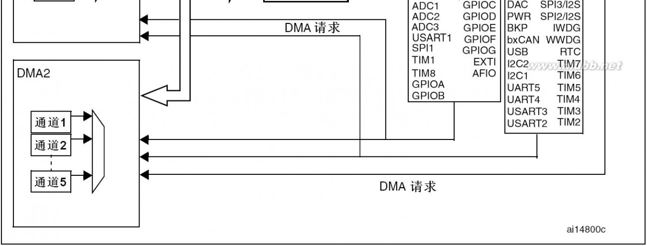
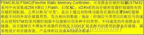
2 系统构架 2.1
在小容量、中容量和 大容量产品中,主系统由以下部分构成:
● 四个驱动单元:
─ Cortex?-M3内核DCode总线(D-bus),和系统总线(S-bus)
─ 通用DMA1和通用DMA2
● 四个被动单元 ─ 内部SRAM
─ 内部闪存存储器
─的桥(AHB2APBx),它连接所有的APB设备
这些都是通过一个多级的AHB总线构架相互连接的,如下图图1所示:
图1 系统结构
在互联型产品中,主系统由以下部分构成:
● 五个驱动单元:
─ Cortex?-M3内核DCode总线(D-bus),和系统总线(S-bus)
─ 通用DMA1和通用DMA2
─ 以太网DMA
● 三个被动单元
─ 内部SRAM
─ 内部闪存存储器
─ AHB到APB的桥(AHB2APBx),它连接所有的APB设备
这些都是通过一个多级的AHB总线构架相互连接的,如图2所示:
25/754
参照2009年12月 RM0008 Reference Manual 英文第10版
本译文仅供参考,如有翻译错误,请以英文原稿为准。(www.61k.com)请读者随时注意在ST网站下载更新版本
stm32 STM32中文参考手册
存储器和总线架构 STM32F10xxx参考手册
图2 互联型产品的系统结构
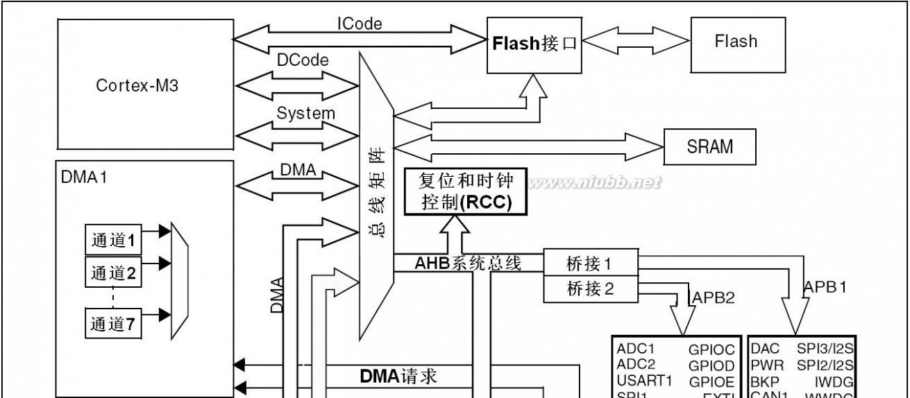
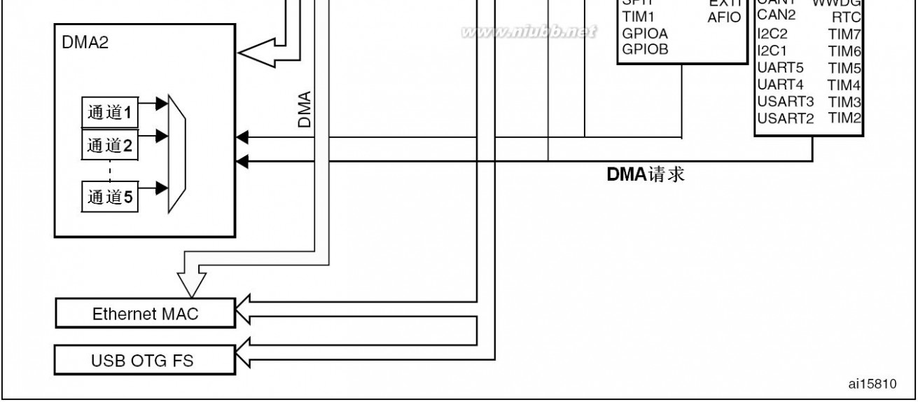
ICode总线
该总线将Cortex?-M3内核的指令总线与闪存指令接口相连接。(www.61k.com]指令预取在此总线上完成。
DCode总线
该总线将Cortex?-M3内核的DCode总线与闪存存储器的数据接口相连接(常量加载和调试访问)。
系统总线
此总线连接Cortex?-M3内核的系统总线(外设总线)到总线矩阵,总线矩阵协调着内核和DMA间的访问。
DMA总线
此总线将DMA的AHB主控接口与总线矩阵相联,总线矩阵协调着CPU的DCode和DMA到 SRAM、闪存和外设的访问。
总线矩阵
总线矩阵协调内核系统总线和DMA主控总线之间的访问仲裁,仲裁利用轮换算法。在互联型产品中,总线矩阵包含5个驱动部件(CPU的DCode、系统总线、以太网DMA、DMA1总线和DMA2总线)和3个从部件(闪存存储器接口(FLITF)、SRAM和AHB2APB桥)。在其它产品中总线矩阵包含4个驱动部件(CPU的DCode、系统总线、DMA1总线和DMA2总线)和4个被动部件(闪存存储器接口(FLITF)、SRAM、FSMC和AHB2APB桥)。
AHB外设通过总线矩阵与系统总线相连,允许DMA访问。
26/754

参照2009年12月 RM0008 Reference Manual 英文第10版
本译文仅供参考,如有翻译错误,请以英文原稿为准。请读者随时注意在ST网站下载更新版本

stm32 STM32中文参考手册
存储器和总线架构 STM32F10xxx参考手册
AHB/APB桥(APB)
两个AHB/APB桥在AHB和2个APB总线间提供同步连接。(www.61k.com]APB1操作速度限于36MHz,APB2操作于全速(最高72MHz)。
有关连接到每个桥的不同外设的地址映射请参考表1。在每一次复位以后,所有除SRAM和FLITF以外的外设都被关闭,在使用一个外设之前,必须设置寄存器RCC_AHBENR来打开该外设的时钟。
注意: 当对APB寄存器进行8位或者16位访问时,该访问会被自动转换成32位的访问:桥会自动将8位
或者32位的数据扩展以配合32位的向量。
2.2 存储器组织

4GB的线性地址空间内。 数据字节以小端格式存放在存储器中。一个字里的最低地址字节被认为是该字的最低有效字节,而最高地址字节是最高有效字节。
外设寄存器的映像请参考相关章节。
可访问的存储器空间被分成8个主要块,每个块为512MB。
其他所有没有分配给片上存储器和外设的存储器空间都是保留的地址空间,请参考相应器件的数据手册中的存储器映像图。
27/754
参照2009年12月 RM0008 Reference Manual 英文第10版
本译文仅供参考,如有翻译错误,请以英文原稿为准。请读者随时注意在ST网站下载更新版本
扩展:stm32中文参考手册 pdf / stm32中文参考手册 v10 / stm32的datebase
stm32 STM32中文参考手册
存储器和总线架构 STM32F10xxx参考手册
2.3 存储器映像
请参考相应器件的数据手册中的存储器映像图。[www.61k.com]表1列出了所用STM32F10xxx中内置外设的起
始地址。 表1
寄存器组起始地址

外设
USB OTG 全速 保留 以太网 保留 CRC
闪存存储器接口 保留
复位和时钟控制(RCC) 保留 DMA2 DMA1 保留 SDIO 保留 ADC3 USART1 TIM8定时器 SPI1 TIM1定时器 ADC2 ADC1 GPIO端口G GPIO端口F GPIO端口E GPIO端口D GPIO端口C GPIO端口B GPIO端口A EXTI AFIO 保留 DAC
电源控制(PWR) 后备寄存器(BKP) bxCAN2 bxCAN1
USB/CAN共享的512字节SRAM
APB1APB2AHBAHB总线
寄存器映像 参见26.14.6节
参见27.8.5节
参见3.4.4节
参见6.3.11节
参见10.4.7节 参见10.4.7节
参见20.9.16节
参见11.12.15节 参见25.6.8节 参见13.4.21节 参见23.5节 参见13.4.21节 参见11.12.15节 参见11.12.15节 参见8.5节 参见8.5节 参见8.5节 参见8.5节 参见8.5节 参见8.5节 参见8.5节 参见9.3.7节 参见8.5节
参见12.5.14节 参见4.4.3节 参见5.4.5节 参见22.9.5节 参见22.9.5节
起始地址
0x5000 0000 – 0x5003 FFFF 0x4003 0000 – 0x4FFF FFFF 0x4002 8000 – 0x4002 9FFF 0x4002 3400 - 0x4002 3FFF 0x4002 3000 - 0x4002 33FF 0x4002 2000 - 0x4002 23FF 0x4002 1400 - 0x4002 1FFF 0x4002 1000 - 0x4002 13FF 0x4002 0800 - 0x4002 0FFF 0x4002 0400 - 0x4002 07FF 0x4002 0000 - 0x4002 03FF 0x4001 8400 - 0x4001 7FFF 0x4001 8000 - 0x4001 83FF 0x4001 4000 - 0x4001 7FFF 0x4001 3C00 - 0x4001 3FFF 0x4001 3800 - 0x4001 3BFF 0x4001 3400 - 0x4001 37FF 0x4001 3000 - 0x4001 33FF 0x4001 2C00 - 0x4001 2FFF 0x4001 2800 - 0x4001 2BFF 0x4001 2400 - 0x4001 27FF 0x4001 2000 - 0x4001 23FF 0x4001 2000 - 0x4001 23FF 0x4001 1800 - 0x4001 1BFF 0x4001 1400 - 0x4001 17FF 0x4001 1000 - 0x4001 13FF 0X4001 0C00 - 0x4001 0FFF 0x4001 0800 - 0x4001 0BFF 0x4001 0400 - 0x4001 07FF 0x4001 0000 - 0x4001 03FF 0x4000 7800 - 0x4000FFFF 0x4000 7400 - 0x4000 77FF 0x4000 7000 - 0x4000 73FF 0x4000 6C00 - 0x4000 6FFF 0x4000 6800 - 0x4000 6BFF 0x4000 6400 - 0x4000 67FF 0x4000 6000(1) - 0x4000 63FF
28/754
参照2009年12月 RM0008 Reference Manual 英文第10版
本译文仅供参考,如有翻译错误,请以英文原稿为准。请读者随时注意在ST网站下载更新版本
stm32 STM32中文参考手册
存储器和总线架构 STM32F10xxx参考手册

0x4000 5C00 - 0x4000 5FFF 0x4000 5800 - 0x4000 5BFF 0x4000 5400 - 0x4000 57FF 0x4000 5000 - 0x4000 53FF 0x4000 4C00 - 0x4000 4FFF 0x4000 4800 - 0x4000 4BFF 0x4000 4400 - 0x4000 47FF 0x4000 4000 - 0x4000 3FFF 0x4000 3C00 - 0x4000 3FFF 0x4000 3800 - 0x4000 3BFF 0x4000 3400 - 0x4000 37FF 0x4000 3000 - 0x4000 33FF 0x4000 2C00 - 0x4000 2FFF 0x4000 2800 - 0x4000 2BFF 0x4000 1800 - 0x4000 27FF 0x4000 1400 - 0x4000 17FF 0x4000 1000 - 0x4000 13FF 0x4000 0C00 - 0x4000 0FFF 0x4000 0800 - 0x4000 0BFF 0x4000 0400 - 0x4000 07FF 0x4000 0000 - 0x4000 03FF
USB全速设备寄存器 I2C2 I2C1 UART5 UART4 USART3 USART2 保留 SPI3/I2S3 SPI2/I2S3 保留
独立看门狗(IWDG) 窗口看门狗(WWDG) RTC 保留 TIM7定时器 TIM6定时器 TIM5定时器 TIM4定时器 TIM3定时器 TIM2定时器
参见21.5.4节 参见24.6.10节 参见24.6.10节 参见25.6.8节 参见25.6.8节 参见25.6.8节 参见25.6.8节
参见23.5节 参见23.5节
参见17.4.5节 参见18.6.4节 参见16.4.7节
参见15.4.9节 参见15.4.9节 参见14.4.19节 参见14.4.19节 参见14.4.19节 参见14.4.19节
1.只在小容量、中容量和大容量的产品中才有这个共享的SRAM区域,互联型产品中没有这个区域。(www.61k.com)
2.3.1 SRAM
内置64K字节的静态(16位)或全字(32位)访问。
SRAM。
2.3.2 位段
Cortex?-M3存储器映像包括两个位段(bit-band)区。这两个位段区将别名存储器区中的每个字映射到位段存储器区的一个位,在别名存储区写入一个字具有对位段区的目标位执行读-改-写操作的相同效果。
在STM32F10xxx里,外设寄存器和SRAM都被映射到一个位段区里,这允许执行单一的位段的写和读操作。
下面的映射公式给出了别名区中的每个字是如何对应位带区的相应位的: bit_word_addr = bit_band_base + (byte_offset×32) + (bit_number×4) 其中:
bit_word_addr是别名存储器区中字的地址,它映射到某个目标位。 bit_band_base是别名区的起始地址。
byte_offset是包含目标位的字节在位段里的序号 bit_number是目标位所在位置(0-31)
例子:
下面的例子说明如何映射别名区中SRAM地址为0x20000300的字节中的位2: 0x22006008 = 0x22000000 + (0x300×32) + (2×4).
对0x22006008地址的写操作与对SRAM中地址0x20000300字节的位2执行读-改-写操作有着相同的效果。
29/754
参照2009年12月 RM0008 Reference Manual 英文第10版
本译文仅供参考,如有翻译错误,请以英文原稿为准。请读者随时注意在ST网站下载更新版本
stm32 STM32中文参考手册
存储器和总线架构 STM32F10xxx参考手册
读0x22006008地址返回SRAM中地址0x20000300字节的位2的值(0x01 或 0x00)。(www.61k.com) 请参考《Cortex?-M3技术参考手册》以了解更多有关位段的信息。
2.3.3 嵌入式闪存
高性能的闪存模块有以下的主要特性:
扩展:stm32中文参考手册 pdf / stm32中文参考手册 v10 / stm32的datebase
● 高达512K字节闪存存储器结构:闪存存储器有主存储块和信息块组成:
─ 主存储块容量:
小容量产品主存储块最大为4K×64位,每个存储块划分为32个1K字节的页(见表2)。 中容量产品主存储块最大为16K×64位,每个存储块划分为128个1K字节的页(见表3)。 大容量产品主存储块最大为64K×64位,每个存储块划分为256个2K字节的页(见表4)。 互联型产品主存储块最大为32K×64位,每个存储块划分为128个2K字节的页(见表5)。 ─ 信息块容量:
互联型产品有2360×64位(见表5)。
其它产品有258×64位(见表2、表3、表4)。 闪存存储器接口的特性为:
● 带预取缓冲器的读接口(每字为2×64位) ● 选择字节加载器 ● 闪存编程/擦除操作 ● 访问/写保护 表2
模块
闪存模块的组织(小容量产品)
名称 页0 页1 页2
地址
0x0800 0000 - 0x0800 03FF 0x0800 0400 - 0x0800 07FF 0x0800 0800 - 0x0800 0BFF 0x0800 0C00 - 0x0800 0FFF 0x0800 1000 - 0x0800 13FF … …
0x0800 7C00 - 0x0800 7FFF 0x1FFF F000 - 0x1FFF F7FF 0x1FFF F800 - 0x1FFF F80F 0x4002 2000 - 0x4002 2003 0x4002 2004 - 0x4002 2007 0x4002 2008 - 0x4002 200B 0x4002 200C - 0x4002 200F 0x4002 2010 - 0x4002 2013 0x4002 2014 - 0x4002 2017 0x4002 2018 - 0x4002 201B 0x4002 201C - 0x4002 201F 0x4002 2020 - 0x4002 2023
大小(字节) 1K 1K 1K 1K 1K … … 1K 2K 16 4 4 4 4 4 4 4 4 4
主存储块
页3 页4 … … 页31 系统存储器 选择字节 FLASH_ACR FALSH_KEYR FLASH_OPTKEYR FLASH_SR FLASH_CR FLASH_AR 保留 FLASH_OBR FLASH_WRPR
信息块
闪存存储器 接口寄存器
30/754

参照2009年12月 RM0008 Reference Manual 英文第10版
本译文仅供参考,如有翻译错误,请以英文原稿为准。请读者随时注意在ST网站下载更新版本
stm32 STM32中文参考手册
存储器和总线架构 STM32F10xxx参考手册
表3
模块
闪存模块的组织(中容量产品)

名称 页0 页1 页2
地址
0x0800 0000 - 0x0800 03FF 0x0800 0400 - 0x0800 07FF 0x0800 0800 - 0x0800 0BFF 0x0800 0C00 - 0x0800 0FFF 0x0800 1000 - 0x0800 13FF …
…
0x0801 FC00 - 0x0801 FFFF 0x1FFF F000 - 0x1FFF F7FF 0x1FFF F800 - 0x1FFF F80F 0x4002 2000 - 0x4002 2003 0x4002 2004 - 0x4002 2007 0x4002 2008 - 0x4002 200B 0x4002 200C - 0x4002 200F 0x4002 2010 - 0x4002 2013 0x4002 2014 - 0x4002 2017 0x4002 2018 - 0x4002 201B 0x4002 201C - 0x4002 201F 0x4002 2020 - 0x4002 2023
大小(字节) 1K 1K 1K 1K 1K … … 1K 2K 16 4 4 4 4 4 4 4 4 4
主存储块
页3 页4 … … 页127 系统存储器 选择字节 FLASH_ACR FALSH_KEYR FLASH_OPTKEYR FLASH_SR FLASH_CR FLASH_AR 保留 FLASH_OBR FLASH_WRPR
信息块
闪存存储器 接口寄存器
表4
模块
闪存模块的组织(大容量产品)
名称 页0 页1 页2
地址
0x0800 0000 - 0x0800 07FF 0x0800 0800 - 0x0800 0FFF 0x0800 1000 - 0x0800 17FF 0x0800 1800 - 0x0800 1FFF … …
0x0807 F800 - 0x0807 FFFF 0x1FFF F000 - 0x1FFF F7FF 0x1FFF F800 - 0x1FFF F80F 0x4002 2000 - 0x4002 2003 0x4002 2004 - 0x4002 2007 0x4002 2008 - 0x4002 200B 0x4002 200C - 0x4002 200F 0x4002 2010 - 0x4002 2013 0x4002 2014 - 0x4002 2017 0x4002 2018 - 0x4002 201B 0x4002 201C - 0x4002 201F 0x4002 2020 - 0x4002 2023
大小(字节) 2K 2K 2K 2K … … 2K 2K 16 4 4 4 4 4 4 4 4 4
主存储块
页3 … … 页255 系统存储器 选择字节 FLASH_ACR FALSH_KEYR FLASH_OPTKEYR FLASH_SR FLASH_CR FLASH_AR 保留 FLASH_OBR FLASH_WRPR
信息块
闪存存储器 接口寄存器
31/754
参照2009年12月 RM0008 Reference Manual 英文第10版
本译文仅供参考,如有翻译错误,请以英文原稿为准。(www.61k.com)请读者随时注意在ST网站下载更新版本
stm32 STM32中文参考手册
[www.61k.com)扩展:stm32中文参考手册 pdf / stm32中文参考手册 v10 / stm32的datebase
本文标题:VBScript程序员参考手册-OpenCV参考手册61阅读| 精彩专题| 最新文章| 热门文章| 苏ICP备13036349号-1